EP0975017A2 - Couche-chapeau d'oxynitrure de silicium pour la fabrication d'une couche diélectrique entre deux métallisations pour de semiconducteurs - Google Patents
Couche-chapeau d'oxynitrure de silicium pour la fabrication d'une couche diélectrique entre deux métallisations pour de semiconducteurs Download PDFInfo
- Publication number
- EP0975017A2 EP0975017A2 EP99113533A EP99113533A EP0975017A2 EP 0975017 A2 EP0975017 A2 EP 0975017A2 EP 99113533 A EP99113533 A EP 99113533A EP 99113533 A EP99113533 A EP 99113533A EP 0975017 A2 EP0975017 A2 EP 0975017A2
- Authority
- EP
- European Patent Office
- Prior art keywords
- layer
- silicon oxynitride
- silicate glass
- fluorinated silicate
- dielectric
- Prior art date
- Legal status (The legal status is an assumption and is not a legal conclusion. Google has not performed a legal analysis and makes no representation as to the accuracy of the status listed.)
- Withdrawn
Links
Images

Classifications
-
- H—ELECTRICITY
- H10—SEMICONDUCTOR DEVICES; ELECTRIC SOLID-STATE DEVICES NOT OTHERWISE PROVIDED FOR
- H10P—GENERIC PROCESSES OR APPARATUS FOR THE MANUFACTURE OR TREATMENT OF DEVICES COVERED BY CLASS H10
- H10P14/00—Formation of materials, e.g. in the shape of layers or pillars
- H10P14/40—Formation of materials, e.g. in the shape of layers or pillars of conductive or resistive materials
-
- H—ELECTRICITY
- H10—SEMICONDUCTOR DEVICES; ELECTRIC SOLID-STATE DEVICES NOT OTHERWISE PROVIDED FOR
- H10P—GENERIC PROCESSES OR APPARATUS FOR THE MANUFACTURE OR TREATMENT OF DEVICES COVERED BY CLASS H10
- H10P14/00—Formation of materials, e.g. in the shape of layers or pillars
- H10P14/60—Formation of materials, e.g. in the shape of layers or pillars of insulating materials
- H10P14/69—Inorganic materials
- H10P14/692—Inorganic materials composed of oxides, glassy oxides or oxide-based glasses
- H10P14/6921—Inorganic materials composed of oxides, glassy oxides or oxide-based glasses containing silicon
- H10P14/6922—Inorganic materials composed of oxides, glassy oxides or oxide-based glasses containing silicon the material containing Si, O and at least one of H, N, C, F or other non-metal elements, e.g. SiOC, SiOC:H or SiONC
- H10P14/6924—Inorganic materials composed of oxides, glassy oxides or oxide-based glasses containing silicon the material containing Si, O and at least one of H, N, C, F or other non-metal elements, e.g. SiOC, SiOC:H or SiONC the material being halogen doped silicon oxides, e.g. FSG
-
- H—ELECTRICITY
- H10—SEMICONDUCTOR DEVICES; ELECTRIC SOLID-STATE DEVICES NOT OTHERWISE PROVIDED FOR
- H10P—GENERIC PROCESSES OR APPARATUS FOR THE MANUFACTURE OR TREATMENT OF DEVICES COVERED BY CLASS H10
- H10P14/00—Formation of materials, e.g. in the shape of layers or pillars
- H10P14/60—Formation of materials, e.g. in the shape of layers or pillars of insulating materials
- H10P14/63—Formation of materials, e.g. in the shape of layers or pillars of insulating materials characterised by the formation processes
- H10P14/6326—Deposition processes
- H10P14/6328—Deposition from the gas or vapour phase
- H10P14/6334—Deposition from the gas or vapour phase using decomposition or reaction of gaseous or vapour phase compounds, i.e. chemical vapour deposition
- H10P14/6336—Deposition from the gas or vapour phase using decomposition or reaction of gaseous or vapour phase compounds, i.e. chemical vapour deposition in the presence of a plasma [PECVD]
-
- H—ELECTRICITY
- H10—SEMICONDUCTOR DEVICES; ELECTRIC SOLID-STATE DEVICES NOT OTHERWISE PROVIDED FOR
- H10P—GENERIC PROCESSES OR APPARATUS FOR THE MANUFACTURE OR TREATMENT OF DEVICES COVERED BY CLASS H10
- H10P14/00—Formation of materials, e.g. in the shape of layers or pillars
- H10P14/60—Formation of materials, e.g. in the shape of layers or pillars of insulating materials
- H10P14/65—Formation of materials, e.g. in the shape of layers or pillars of insulating materials characterised by treatments performed before or after the formation of the materials
- H10P14/6502—Formation of materials, e.g. in the shape of layers or pillars of insulating materials characterised by treatments performed before or after the formation of the materials of treatments performed before formation of the materials
- H10P14/6506—Formation of intermediate materials
-
- H—ELECTRICITY
- H10—SEMICONDUCTOR DEVICES; ELECTRIC SOLID-STATE DEVICES NOT OTHERWISE PROVIDED FOR
- H10P—GENERIC PROCESSES OR APPARATUS FOR THE MANUFACTURE OR TREATMENT OF DEVICES COVERED BY CLASS H10
- H10P14/00—Formation of materials, e.g. in the shape of layers or pillars
- H10P14/60—Formation of materials, e.g. in the shape of layers or pillars of insulating materials
- H10P14/65—Formation of materials, e.g. in the shape of layers or pillars of insulating materials characterised by treatments performed before or after the formation of the materials
- H10P14/6516—Formation of materials, e.g. in the shape of layers or pillars of insulating materials characterised by treatments performed before or after the formation of the materials of treatments performed after formation of the materials
- H10P14/6548—Formation of materials, e.g. in the shape of layers or pillars of insulating materials characterised by treatments performed before or after the formation of the materials of treatments performed after formation of the materials by forming intermediate materials, e.g. capping layers or diffusion barriers
-
- H—ELECTRICITY
- H10—SEMICONDUCTOR DEVICES; ELECTRIC SOLID-STATE DEVICES NOT OTHERWISE PROVIDED FOR
- H10P—GENERIC PROCESSES OR APPARATUS FOR THE MANUFACTURE OR TREATMENT OF DEVICES COVERED BY CLASS H10
- H10P14/00—Formation of materials, e.g. in the shape of layers or pillars
- H10P14/60—Formation of materials, e.g. in the shape of layers or pillars of insulating materials
- H10P14/66—Formation of materials, e.g. in the shape of layers or pillars of insulating materials characterised by the type of materials
- H10P14/668—Formation of materials, e.g. in the shape of layers or pillars of insulating materials characterised by the type of materials the materials being characterised by the deposition precursor materials
- H10P14/6681—Formation of materials, e.g. in the shape of layers or pillars of insulating materials characterised by the type of materials the materials being characterised by the deposition precursor materials the precursor containing a compound comprising Si
- H10P14/6682—Formation of materials, e.g. in the shape of layers or pillars of insulating materials characterised by the type of materials the materials being characterised by the deposition precursor materials the precursor containing a compound comprising Si the compound being a silane, e.g. disilane, methylsilane or chlorosilane
-
- H—ELECTRICITY
- H10—SEMICONDUCTOR DEVICES; ELECTRIC SOLID-STATE DEVICES NOT OTHERWISE PROVIDED FOR
- H10P—GENERIC PROCESSES OR APPARATUS FOR THE MANUFACTURE OR TREATMENT OF DEVICES COVERED BY CLASS H10
- H10P14/00—Formation of materials, e.g. in the shape of layers or pillars
- H10P14/60—Formation of materials, e.g. in the shape of layers or pillars of insulating materials
- H10P14/69—Inorganic materials
- H10P14/692—Inorganic materials composed of oxides, glassy oxides or oxide-based glasses
- H10P14/6921—Inorganic materials composed of oxides, glassy oxides or oxide-based glasses containing silicon
- H10P14/6922—Inorganic materials composed of oxides, glassy oxides or oxide-based glasses containing silicon the material containing Si, O and at least one of H, N, C, F or other non-metal elements, e.g. SiOC, SiOC:H or SiONC
- H10P14/6927—Inorganic materials composed of oxides, glassy oxides or oxide-based glasses containing silicon the material containing Si, O and at least one of H, N, C, F or other non-metal elements, e.g. SiOC, SiOC:H or SiONC the material being a silicon oxynitride, e.g. SiON or SiON:H
-
- H—ELECTRICITY
- H10—SEMICONDUCTOR DEVICES; ELECTRIC SOLID-STATE DEVICES NOT OTHERWISE PROVIDED FOR
- H10W—GENERIC PACKAGES, INTERCONNECTIONS, CONNECTORS OR OTHER CONSTRUCTIONAL DETAILS OF DEVICES COVERED BY CLASS H10
- H10W20/00—Interconnections in chips, wafers or substrates
- H10W20/01—Manufacture or treatment
- H10W20/071—Manufacture or treatment of dielectric parts thereof
-
- H—ELECTRICITY
- H10—SEMICONDUCTOR DEVICES; ELECTRIC SOLID-STATE DEVICES NOT OTHERWISE PROVIDED FOR
- H10W—GENERIC PACKAGES, INTERCONNECTIONS, CONNECTORS OR OTHER CONSTRUCTIONAL DETAILS OF DEVICES COVERED BY CLASS H10
- H10W20/00—Interconnections in chips, wafers or substrates
- H10W20/01—Manufacture or treatment
- H10W20/071—Manufacture or treatment of dielectric parts thereof
- H10W20/074—Manufacture or treatment of dielectric parts thereof of dielectric parts comprising thin functional dielectric layers, e.g. dielectric etch-stop, barrier, capping or liner layers
-
- H—ELECTRICITY
- H10—SEMICONDUCTOR DEVICES; ELECTRIC SOLID-STATE DEVICES NOT OTHERWISE PROVIDED FOR
- H10W—GENERIC PACKAGES, INTERCONNECTIONS, CONNECTORS OR OTHER CONSTRUCTIONAL DETAILS OF DEVICES COVERED BY CLASS H10
- H10W20/00—Interconnections in chips, wafers or substrates
- H10W20/01—Manufacture or treatment
- H10W20/071—Manufacture or treatment of dielectric parts thereof
- H10W20/081—Manufacture or treatment of dielectric parts thereof by forming openings in the dielectric parts
-
- H—ELECTRICITY
- H10—SEMICONDUCTOR DEVICES; ELECTRIC SOLID-STATE DEVICES NOT OTHERWISE PROVIDED FOR
- H10W—GENERIC PACKAGES, INTERCONNECTIONS, CONNECTORS OR OTHER CONSTRUCTIONAL DETAILS OF DEVICES COVERED BY CLASS H10
- H10W20/00—Interconnections in chips, wafers or substrates
- H10W20/40—Interconnections external to wafers or substrates, e.g. back-end-of-line [BEOL] metallisations or vias connecting to gate electrodes
- H10W20/45—Interconnections external to wafers or substrates, e.g. back-end-of-line [BEOL] metallisations or vias connecting to gate electrodes characterised by their insulating parts
- H10W20/48—Insulating materials thereof
-
- H—ELECTRICITY
- H10—SEMICONDUCTOR DEVICES; ELECTRIC SOLID-STATE DEVICES NOT OTHERWISE PROVIDED FOR
- H10W—GENERIC PACKAGES, INTERCONNECTIONS, CONNECTORS OR OTHER CONSTRUCTIONAL DETAILS OF DEVICES COVERED BY CLASS H10
- H10W74/00—Encapsulations, e.g. protective coatings
- H10W74/10—Encapsulations, e.g. protective coatings characterised by their shape or disposition
- H10W74/131—Encapsulations, e.g. protective coatings characterised by their shape or disposition the semiconductor body being only partially enclosed
- H10W74/147—Encapsulations, e.g. protective coatings characterised by their shape or disposition the semiconductor body being only partially enclosed the encapsulations being multilayered
Definitions
- This invention relates to a semiconductor device that includes a silicon oxynitride cap for a fluorinated silicate glass (FSG) film in intermetal dielectric; semiconductor fabrication, and more particularly to a stable combination arrangement of a FSG film covered by a silicon oxynitride cap layer on a semiconductor substrate, as well as to a method of manufacturing a semiconductor device that includes forming a patterned conductive, i.e., electrically conductive, layer on a semiconductor substrate with a FSG film combined with a silicon oxynitride cap layer for intermetal dielectric application.
- a patterned conductive i.e., electrically conductive
- the insulation layers e.g., of silicon dioxide, silicon oxynitride (SiO x N y ), fluorinated silicate glass (FSG), also called fluorinated silicon oxide, spin-on glass (SOG), etc., serve as electrical insulation between metal layers, e.g., intermetal dielectric (IMD) layers, as protective layers, as gap filling layers to achieve planarization (layer flatness) in the wafer substrate, and the like, as the case may be.
- the individual layers are deposited by conventional technique such as plasma enhanced chemical vapor deposition (PECVD), atmospheric pressure CVD, etc.
- a first level metal layer e.g., disposed on a silicon substrate containing devices, is separated by one or more insulation layers from a second level metal layer thereabove. This in turn may be separated by one or more further insulation layers from a third level metal layer thereabove, etc.
- These metal layers are interconnected by metallization through vias or small holes or apertures etched in the intervening insulation layers.
- the stacked layers undergo photolithographic processing to provide a pattern thereon consonant with the IC design, e.g., to form vias.
- the top layer on the wafer substrate is covered with a photoresist layer of photo-reactive polymeric material for patterning via a mask.
- Light such as visible or ultraviolet (UV) light is directed through the mask onto the photoresist layer to expose it in the mask pattern.
- the polymeric material of the photoresist layer is transparent to the light yet photo-reactive to change its chemical properties, i.e., by photo-initiated reaction, thereby permitting its patterning.
- An antireflective coating (ARC) layer such as an organic ARC layer, e.g., of light absorbing polymer, such as polyimide, is usually provided at the top portion of the wafer substrate to minimize reflection of light back to the photoresist layer for more uniform processing.
- ARC antireflective coating
- the photoresist may be of negative or positive type.
- a negative photoresist the exposed (polymerized) areas become insoluble while the unexposed (unpolymerized) areas dissolve in a later applied developer liquid.
- a positive photoresist the exposed (degraded) soluble areas dissolve in the developer liquid while the unexposed (insoluble) areas remain.
- the photoresist material remaining on the wafer substrate forms the pattern to serve as a mask for etching in turn of the pertinent layers.
- etching process is also different therefrom, e.g., in forming vias in dielectric layers to connect neighboring level metal layers.
- the etching is desirably anisotropic (high rate vertical direction etching and low rate or inhibited horizontal direction etching), as distinguished from isotropic (etching the exposed surfaces equally in all directions), for providing an etched structure of uniform vertical wall geometry or profile.
- Etching may be effected by wet etching (solution) or dry etching (plasma etching or reactive ion etching) technique, depending on the physical and chemical characteristics of the material being etched and of the neighboring material.
- VLSI very large scale integration
- visible light has a wavelength spectrum of 400-700 nm (4,000-7,000 angstroms)
- UV light has a wavelength spectrum of 100-400 nm (1,000-4,000 angstroms).
- mid UV (MUV) light has a wavelength of about 365 nm
- deep UV (DUV) light has a wavelength of about 248 nm or less.
- the desired high aspect ratios (depth to width) associated with photolithographic processing to form apertures or windows, fine conductive lines, etc., in various layers of the wafer substrate require very strict tolerances to prevent undesired defects such as touching of closely spaced apart components that can cause short circuiting,,etc.
- Contaminants that are incompatible with the photo-reactive polymeric material can migrate into the photoresist layer from the ARC layer or other vicinal layer. These contaminants can poison the photoresist layer, e.g., undergo interfering reactions therewith, causing non-uniformity of the reaction therein by extraneous chemical interaction with the polymeric material. This is commonly called photoresist poisoning.
- FSG fluorinated silicate glass
- IMD intermetal dielectric
- CVD chemical vapor deposition
- PECVD plasma enhanced chemical vapor deposition
- the dielectric constant achievable for FSG is about 3.3 depending on the fluorine concentration in the FSG film and the precursor used to deposit the FSG film.
- a higher fluorine concentration usually provides a lower dielectric constant.
- a higher fluorine concentration makes the film unstable because free fluorine tends to diffuse or migrate out of the film to adjacent layers in the IC.
- FSG fluorine substances
- fluorine substances including fluorine itself and attendant self-generating contaminant compounds thereof with other contaminating precursor constituents
- FSG use is combined with post plasma treatment, e.g., plasma treatment using oxygen and nitrogen or nitrous oxide (N 2 O), or the inclusion of a silicon dioxide cap layer to minimize fluorine substance out diffusion.
- post plasma treatment e.g., plasma treatment using oxygen and nitrogen or nitrous oxide (N 2 O)
- N 2 O nitrogen or nitrous oxide
- fluorine substances, including fluorine itself will diffuse well into silicon dioxide films and the diffusion length (penetration depth) thereof can be in excess of several thousand angstroms.
- fluorine substance contemplates fluorine-containing substances including both free fluorine itself and attendant self-generating contaminant compounds thereof with other contaminating precursor constituents such as hydrogen and nitrogen (i.e., fluorine-containing contaminant compounds).
- a typical semiconductor fabrication technique using FSG as a low dielectric material for IMD application includes the steps of:
- the foregoing drawbacks are obviated in accordance with the present invention by providing a system of a fluorinated silicate glass (FSG) film (layer) combined with a silicon oxynitride (SiO x N y ) cap layer for intermetal dielectric (IMD) application in semiconductor fabrication.
- FSG fluorinated silicate glass
- SiO x N y silicon oxynitride
- IMD intermetal dielectric
- a semiconductor device that includes a substrate having a combination of a FSG layer, e.g., of about 1,000-10,000 angstroms thickness, and a silicon oxynitride cap layer, e.g., of about 100-1,000 angstroms thickness, thereon.
- the silicon oxynitride cap layer is disposed in overlying covering relation to the FSG layer sufficiently to prevent fluorine substance outflow therethrough from the FSG layer and to form an antireflective coating (ARC).
- a conductive layer e.g., of a metal such as aluminum, tungsten or copper, is disposed in overlying relation to the silicon oxynitride cap layer.
- the silicon oxynitride cap layer is arranged relative to the underlying FSG layer and overlying conductive layer sufficiently to prevent fluorine substance outflow therethrough from the FSG layer to the conductive layer.
- the semiconductor device includes a substrate that has a patterned conductive layer, e.g., of a metal such as aluminum, tungsten or copper, thereon, a dielectric liner, e.g., an IMD liner of silicon dioxide, disposed on the patterned conductive layer, and a combination of a FSG layer and a silicon oxynitride cap layer disposed on the dielectric liner, the silicon oxynitride cap layer being disposed in overlying covering relation to the FSG layer.
- a further conductive layer e.g., of a metal such as aluminum, tungsten or copper, is disposed in overlying relation to the silicon oxynitride cap layer and in conductive contact with the patterned conductive layer.
- the silicon oxynitride cap layer is arranged relative to the underlying FSG layer and overlying further conductive layer sufficiently to prevent fluorine substance outflow therethrough from the FSG layer to the further conductive layer.
- a method for forming a patterned conductive layer on a semiconductor substrate comprises providing a conductive layer, e.g., of aluminum, tungsten or copper, on a surface of a semiconductor substrate, a dielectric liner, e.g., an IMD liner of silicon dioxide, on the conductive layer, a FSG layer on the dielectric liner, and a silicon oxynitride layer on the FSG layer sufficient to prevent fluorine substance outflow therethrough from the FSG layer and to form an antireflective coating (ARC).
- a photoresist layer is provided on the silicon oxynitride layer.
- the photoresist layer is selectively exposed and developed to uncover selective pattern portions of the underlying silicon oxynitride layer.
- the pattern portions of the silicon oxynitride layer and corresponding underlying portions of the FSG and dielectric liner are removed to expose pattern portions of the conductive layer such as for metallization.
- the uncovered pattern portions of the silicon oxynitride layer and corresponding underlying portions of the FSG layer and dielectric liner are desirably all removed together in an etching step such as a dry etching step, e.g., by contact etching in a single dry etching step using CF 4 (tetrafluoromethane) and argon gas per RIE (reactive ion etching).
- a dry etching step e.g., by contact etching in a single dry etching step using CF 4 (tetrafluoromethane) and argon gas per RIE (reactive ion etching).
- a dielectric cap layer is preferably provided between the FSG and silicon oxynitride layers, e.g., in a thickness up to about 20,000 angstroms, for gap-filling, spacing and planarizing purposes.
- the dielectric cap layer is desirably polished, such as by a conventional chemical mechanical polishing (CMP) step, before the silicon oxynitride layer is provided thereon.
- CMP chemical mechanical polishing
- the polished dielectric cap layer typically has a resultant thickness of about 0-20,000 angstroms.
- the uncovered pattern portions of the silicon oxynitride layer and corresponding underlying portions of the dielectric cap layer, FSG layer and dielectric liner are advantageously all removed together in the etching step.
- the conductive layer is provided in a thickness of about 1,000-10,000 angstroms
- the dielectric liner is provided in a thickness of about 100-2,000 angstroms
- the FSG layer is provided in a thickness of about 1,000-10,000 angstroms
- the silicon oxynitride layer is provided in a thickness of about 100-2,000 angstroms.
- the silicon oxynitride comprises SiO 0.5-1.5 N 0.1-1.5 .
- the photoresist layer may be exposed to light irradiation at a wavelength of about 193-633 nm (UV and visible light).
- the silicon oxynitride layer typically has a refractive index of about 1.60-3.6 and an extinction coefficient of about 0.01-2.0.
- the method comprises the steps of providing a conductive metal layer on a surface of a semiconductor substrate, a dielectric silicon dioxide liner on the conductive layer, a FSG layer on the dielectric liner, a dielectric silicon dioxide cap layer on the FSG layer, and a silicon oxynitride layer on the dielectric cap layer and in overlying relation to the FSG layer sufficient to prevent fluorine substance outflow therethrough from the FSG layer and to form an ARC.
- a photoresist layer is provided on the silicon oxynitride layer.
- Further steps comprise selectively exposing and developing the photoresist layer to uncover selective pattern portions of the underlying silicon oxynitride layer, and collectively removing together the uncovered pattern portions of the silicon oxynitride layer and corresponding underlying portions of the dielectric cap layer, FSG layer and dielectric liner in a single etching step to expose pattern portions of the conductive layer such as for metallization.
- the dielectric cap layer is polished by a CMP step before the silicon oxynitride layer is provided thereon.
- a method of treating a wafer substrate in semiconductor fabrication for preventing fluorine substance outflow from a FSG layer thereon to an overlying photoresist layer and simultaneously for suppressing reflection of light waves back into the photoresist layer during photolithographic processing of the photoresist layer to maximize uniformity of patterned light wave exposure and development of the photoresist layer.
- the method comprises interposing a silicon oxynitride layer between the FSG layer and the photoresist layer sufficiently to form a barrier for preventing said fluorine substance outflow and to form a dielectric ARC in underlying relation to the photoresist layer for suppressing said reflection of light waves.
- the present invention also contemplates the product thereby produced.
- FIGS. 1A to 1G there are shown stages of fabrication of a PRIOR ART semiconductor device or microchip 20 having variously a wafer substrate 21, a metal conductive layer 22, a silicon dioxide intermetal dielectric liner 23, a dielectric FSG layer 24, a FSG layer polished top surface 24b, a silicon dioxide dielectric cap layer 25, a silicon dioxide cap layer rough top surface 25a and polished top surface 25b, an additional silicon dioxide dielectric cap layer 26, an organic ARC layer 27, a photoresist layer 28, e.g., of positive photoresist material, a contact hole (aperture) 29, a deepened contact hole 29a and a via (aperture) 30.
- a photoresist layer 28 e.g., of positive photoresist material
- FIGS. 1A to 1G illustrate a typical PRIOR ART method sequence of ten steps for forming a patterned conductive layer on a semiconductor substrate, using FSG as an IMD material.
- FIG. 1A shows semiconductor device or microchip 20 having a wafer substrate 21 on which have been sequentially deposited by known PECVD technique a metal conductive layer 22, a silicon dioxide intermetal dielectric liner 23 for metal layer 22, a FSG layer 24 as a low dielectric material to separate neighboring levels of metallization, and a silicon dioxide dielectric cap layer 25 for dielectric FSG layer 24 as a topographically conformal covering and spacing material to fill in step unevenness and gaps, level off the surface of FSG layer 24 and partially reduce fluorine substance out diffusion (including out diffusion of fluorine itself) from FSG layer 24.
- silicon dioxide cap layer 25 which serves as a planarizing layer, has a rough top surface 25a.
- FIG. 1B shows semiconductor device 20 with rough top surface 25a and a portion of the upper course of silicon dioxide cap layer 25 removed to provide polished top surface 25b thereon flush with the adjacent top course of FSG layer 24 which is concomitantly provided with polished top surface 24b for planarizing purposes.
- This is the condition of semiconductor device 20 after the step of (5) chemical mechanical polishing (CMP) of silicon dioxide cap layer 25 and concomitantly of FSG layer 24.
- CMP chemical mechanical polishing
- FIG. 1C shows semiconductor device 20 with additional post CMP silicon dioxide dielectric cap layer 26 on the corresponding polished top surface 25b of silicon dioxide cap layer 25 and concomitantly on polished top surface 24b of FSG layer 24. This is the condition of semiconductor device 20 after the step of (6) depositing post CMP additional silicon dioxide cap layer 26 on polished silicon dioxide cap layer 25 and concomitantly on polished FSG layer 24.
- FIG. 1D shows semiconductor device 20 with organic ARC layer 27 on additional silicon dioxide cap layer 26 and photoresist layer 28, e.g., of positive photoresist material, on organic ARC layer 27, just prior to photolithographic exposure.
- This is the condition of semiconductor device 20 after the step of (7) depositing organic ARC layer 27 on additional post CMP silicon dioxide cap layer 26, and the first part of step (8), i.e., depositing photoresist layer 28 on organic ARC layer 27.
- FIG. 1E shows semiconductor device 20 after photolithographic exposure of photoresist layer 28 through a patterned mask (not shown) and subsequent development in known manner, to form contact hole (aperture) 29. This is the condition of semiconductor device 20 after the remaining part of step (8), i.e., photolithographic exposure and development.
- FIG. 1F shows semiconductor device 20 after the first etching step in which organic ARC layer 27 is subjected to an open etch to form deepened contact hole 29a. This is the condition of semiconductor device 20 after the step of (9) open etching of organic ARC layer 27.
- FIG. 1G shows semiconductor device 20 after the second etching step in which the vicinal portions of additional silicon dioxide cap layer 26, silicon dioxide cap layer 25 (if any), FSG layer 24 and silicon dioxide liner 23 are subjected to contact etching to form via (aperture) 30 for exposing metal layer 22 for metallization and further processing.
- This is the condition of semiconductor device 20 after the final step of (10) contact etching the vicinal dielectric layers 26, 25 (if any), 24 and 23.
- the steps of depositing on wafer substrate 21 of metal layer 22, silicon dioxide liner 23, FSG layer 24 and silicon dioxide cap layer 25, then polishing silicon dioxide cap layer 25 and FSG layer 24, and further depositing additional silicon dioxide cap layer 26, organic ARC layer 27, and photoresist layer 28, are effected by conventional technique.
- the further steps of photolithographically exposing and developing photoresist layer 28, etching organic ARC layer 27, and etching additional silicon dioxide cap layer 26, silicon dioxide cap layer 25 (where present), FSG layer 24 and silicon dioxide liner 23, to expose metal layer 22, are also effected by conventional technique.
- organic ARC layer 27 must be provided as a separate additional layer and the above discussed ten step prior art method requires two separate etching steps. This is because organic ARC layer 27 cannot be etched by the contact etch needed to etch silicon dioxide based dielectric layers 26, 25 (where present), 24 and 23. Conversely, silicon dioxide based dielectric layers 26, 25 (where present), 24 and 23 cannot be etched by the open etch needed to etch organic ARC layer 27. As demonstrated below, these prior art drawbacks are overcome by the system of the present invention.
- the method of forming a patterned conductive layer on a semiconductor substrate contemplates the analogous eight steps of:
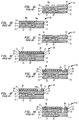
- FIGS. 2A to 2F there are shown stages of fabrication of a semiconductor device or microchip 40 according to an embodiment of the invention, having variously a wafer substrate 21', e.g., of silicon, a conductive layer 22', e.g., of a metal, an IMD (intermetal dielectric) liner 23', e.g., of silicon dioxide, a dielectric FSG (fluorinated silicate glass) layer 24', a FSG layer polished top surface 24b', a silicon dioxide cap layer 25', a silicon dioxide cap layer rough top surface 25a' and polished top surface 25b', a dielectric silicon oxynitride ARC cap layer 41, a photoresist layer 42, e.g., of positive photoresist material, a contact hole (aperture) 43, and a via (aperture) 44.
- a wafer substrate 21' e.g., of silicon
- a conductive layer 22' e.g., of a metal
- FIGS. 2A to 2F parts having prime (') designations are the same as those in FIGS. 1A to 1G.
- FIGS. 2A to 2F illustrate a method sequence of eight steps for forming a patterned conductive layer on a semiconductor substrate, using FSG as an IMD material.
- FIG. 2A shows semiconductor device or microchip 40 having a wafer substrate 21' on which have been sequentially deposited by known PECVD technique a conductive layer 22', e.g., of a metal, an IMD (intermetal dielectric) liner 23', e.g., of silicon dioxide, for metal layer 22', a FSG layer 24' as a low dielectric material to separate neighboring levels of metallization, and a silicon dioxide cap layer 25' for FSG layer 24' as a topographically conformal covering and spacing material to fill in step unevenness and gaps, level off the surface of FSG layer 24' and partially reduce fluorine substance out diffusion from FSG layer 24'.
- a conductive layer 22' e.g., of a metal
- IMD (intermetal dielectric) liner 23' e.g., of silicon dioxide
- FSG layer 24' as a low dielectric material to separate neighboring levels of metallization
- silicon dioxide cap layer 25' for FSG layer 24' as a topographic
- silicon dioxide cap layer 25' which serves as a planarizing layer, has a rough top surface 25a'. This is the condition of semiconductor device 40 after the steps of [1] depositing and patterning metal layer 22 on wafer substrate 21, [2] depositing silicon dioxide liner 23 on metal layer 22, [3] depositing FSG layer 24 on silicon dioxide liner 23, and [4] depositing gap-filling and planarizing silicon dioxide cap layer 25 on FSG layer 24.
- FIG. 2B shows semiconductor device 40 with rough top surface 25a' and a portion of the upper course of silicon dioxide cap layer 25' removed to provide polished top surface 25b' thereon flush with the adjacent top course of FSG layer 24' which is concomitantly provided with polished top surface 24b' for planarizing purposes.
- This is the condition of semiconductor device 40 after the step of [5] effecting chemical mechanical polishing (CMP) of silicon dioxide cap layer 25' and concomitantly of the adjacent portions of FSG layer 24'.
- CMP chemical mechanical polishing
- FIG. 2C shows semiconductor device 40 with a post CMP silicon oxynitride ARC cap layer 41 on the corresponding polished top surface 25b' of silicon dioxide cap layer 25' and concomitantly on polished top surface 24b' of FSG layer 24', and which is sufficient (i.e., in thickness and density) to prevent fluorine substance outflow therethrough from FSG layer 24' and for forming an ARC.
- This is the condition of semiconductor device 40 after the step of [6] depositing post CMP silicon oxynitride ARC cap layer 41 on polished silicon dioxide cap layer 25' and concomitantly on polished FSG layer 24'.
- FIG. 2D shows semiconductor device 40 with photoresist layer 42, e.g., of positive photoresist material, on silicon oxynitride ARC layer 41, just prior to photolithographic exposure. This is the condition of semiconductor device 40 after the first part of step [7], i.e., depositing photoresist layer 42 on silicon oxynitride ARC layer 41.
- photoresist layer 42 e.g., of positive photoresist material
- FIG. 2E shows semiconductor device 40 after photolithographic exposure of photoresist layer 42 through a patterned mask (not shown) and subsequent development in known manner, to form contact hole (aperture) 43.
- This is the condition of semiconductor device 40 after the remaining part of step [7], i.e., selective photolithographic exposure and development to uncover selective pattern portions of the underlying silicon oxynitride ARC layer 41.
- FIG. 2F shows semiconductor device 40 after the single etching step in which the vicinal portions of silicon oxynitride ARC layer 41, silicon dioxide cap layer 25' (if any), FSG layer 24' and silicon dioxide liner 23' are subjected to contact etching to form via (aperture) 44 to expose metal layer 22' for metallization and further processing.
- This is the condition of semiconductor device 40 after the final step of [8] contact etching of the vicinal dielectric layers 41, 25' (where present), 24' and 23' to remove the uncovered pattern portions of silicon oxynitride ARC layer 41 and corresponding portions of silicon dioxide cap layer 25' (if any), FSG layer 24' and silicon dioxide liner 23' to expose patterned portions of metal layer 22.
- Such may be effected by contact etching in a single dry etching step, e.g., using CF 4 (tetrafluoromethane) and argon gas per RIE (reactive ion etching).
- the further steps of photolithographically exposing and developing photoresist layer 42, and then etching collectively dielectric silicon oxynitride ARC layer 41, silicon dioxide cap layer 25' (where present), FSG layer 24' and silicon dioxide liner 23' to expose metal layer 22', are also effected by conventional technique.
- metal layer 22', silicon dioxide liner 23', FSG layer 24', silicon dioxide cap layer 25' and silicon oxynitride ARC layer 41 are typically provided by PECVD technique.
- FSG layer 24' can also be provided by HDP type CVD.
- metal layer 22' is provided in a thickness of about 1,000-10,000 angstroms
- silicon dioxide liner 23' is provided in a thickness of about 100-2,000 angstroms
- FSG layer 24' is provided in a thickness of about 1,000-10,000 angstroms
- silicon dioxide cap layer 25' is provided in a thickness of up to about 20,000 angstroms (i.e., about 0-20,000 angstroms)
- silicon oxynitride ARC layer 41 is provided in a thickness of about 100-2,000 angstroms.
- Photoresist layer 42 is exposed to UV or visible light wave irradiation such as at a wavelength of about 193 to 633 nm.
- silicon oxynitride ARC layer 41 has a refractive index of about 1.60-3.6 (real part) at said wavelength and an extinction coefficient of about 0.01 to 2.0 (imaginary part) at said wavelength.
- silicon oxynitride ARC layer 41 may be provided in a suitable thickness on FSG layer 24' to suppress out diffusion of fluorine substances (including fluorine itself and attendant self-generating contaminant compounds thereof with other contaminating precursor constituents) from FSG layer 24' to the interface with adjacent metal layers such as those applied during subsequent metallization operations. This will insure against metal layer peeling due to collection of fluorine and contaminant compounds thereof, out diffused from FSG layer 24' to a neighboring metal interface and acting as corroding or poisoning agents thereat.
- fluorine substances including fluorine itself and attendant self-generating contaminant compounds thereof with other contaminating precursor constituents
- the silicon oxynitride ARC layer thus achieves increased stability of the FSG layer for IMD application, compared to silicon dioxide, by providing a better protective diffusion barrier to outflow of fluorine substances from the underlying FSG layer, even when used in a layer thickness of only about 100-2,000 angstroms. This is due to the fact that silicon oxynitride is a much denser material than FSG. This effectively prevents metal peeling problems caused by fluorine substance out-gassing as encountered in the prior art.
- silicon oxynitride as contemplated herein, is absorptive of light at all pertinent wavelengths, e.g., 193-633 nm, having a refractive index of 1.6-3.6 (real part) and an extinction coefficient of 0.01-2.0 (imaginary part) at 193-633 nm wavelength, it serves as an efficient in situ ARC for photoresist layer 42. Specifically, it promotes complete and uniform photolithographic exposure and development of the IC design pattern areas at high aspect ratios (depth to width) for producing photoresist footing-free and photoresist pinching-free profiles, i.e., essentially straight vertical walls in the etched areas.
- the silicon oxynitride ARC layer thus simultaneously also achieves uniform reflectance control for contact photolithographic processing since it is an excellent antireflective material for both MUV (typically of 365 nm wavelength) and DUV (typically of 248 nm or less wavelength) photolithographic processing.
- the silicon oxynitride composition can be adjusted to optimize its antireflective property by suitably changing the composition ratio of the SiO x N y components, where x is 0.5-1.5 and y is 0.1-1.5, i.e., SiO 0.5-1.5 N 0.1-1.5 , for example, per PECVD using silane (SiH 4 ) with nitrous oxide (N 2 O) or oxygen and nitrogen. More particularly, the silicon oxynitride comprises SiO 0.5-1.5 N 0.1-1.5 , and antireflective material of three phases including an amorphorous silicon phase, a silicon oxide phase, and a silicon nitride phase.
- wafer substrate 21' may be made of silicon, or of another material such as a metal.
- Metal layer 22' is typically made of aluminum, tungsten or copper.
- Silicon dioxide liner 23' serves as an insulation barrier between metal layer 22' and FSG layer 24'.
- Silicon dioxide layer 25' is provided as a conventional spacing material to contribute thickness before planarizing polishing of FSG layer 24' such as by CMP to improve the flatness of FSG layer 24'. These materials are sufficiently refractory to withstand subsequent metallization and further processing at elevated temperatures of at least about 420°C.
- the ten step prior art method suffers from the disadvantages of inadequate suppression of fluorine substance out diffusion from FSG layer 24 using additional silicon dioxide cap layer 26, plus the need for an additional organic ARC layer 27 and for two incompatible etching steps, one for organic ARC layer 27 and the other for silicon dioxide based dielectric layers 26, 25 (where present), 24 and 23.
- silicon oxynitride ARC layer 41 is a dielectric material like the dielectric material of silicon dioxide cap layer 25', FSG layer 24' and silicon dioxide liner 23', all of these layers may be etched collectively in a single etching step to expose metal layer 22' such as by contact etching using a dry etching step.
- the prior art method of providing a conventional ARC layer can be skipped because silicon oxynitride ARC layer 41 which serves as such ARC can be etched away using similar chemistry to silicon dioxide dielectric etching, enabling use of a single step contact etch process, which does not contemplate an ARC open etch process.
- the wafer substrate may undergo the back end of the line steps remaining between metallization and sale.
- FIG. 3 shows semiconductor device 40 after stripping photoresist layer 42 (FIG. 2F), depositing a further insulation layer 45 on silicon oxynitride ARC layer 41, and etching a trench 46 in further insulation layer 45.
- a further (second level) conductive layer 47 e.g., of aluminum, tungsten or copper, such as in a layer thickness of about 1,000-10,000 angstroms, in trench 46 and in conductive contact with (first level) conductive layer 22' through via 44. All these steps are effected by conventional technique.
- trench 46 which is defined in further insulation layer 45, and further conductive layer 47, which extends along trench 46, collectively run in a direction perpendicular to the plane of the paper of FIG. 3.
- the combination of FSG layer 24' and silicon oxynitride ARC layer 41 provides semiconductor device 40 with an arrangement for preventing fluorine substance outflow from FSG layer 24' to further conductive layer 47 (FIG. 3) in accordance with the invention.
- the combination of FSG layer 24' and silicon oxynitride ARC layer 41 forms an in situ ARC construction (FIG. 2C) for efficient sub-quarter micron photolithographic processing of semiconductor device 40 as generally described above in connection with FIGS. 2A to 2F.
Landscapes
- Internal Circuitry In Semiconductor Integrated Circuit Devices (AREA)
- Exposure Of Semiconductors, Excluding Electron Or Ion Beam Exposure (AREA)
- Formation Of Insulating Films (AREA)
Applications Claiming Priority (2)
| Application Number | Priority Date | Filing Date | Title |
|---|---|---|---|
| US120630 | 1998-07-22 | ||
| US09/120,630 US6300672B1 (en) | 1998-07-22 | 1998-07-22 | Silicon oxynitride cap for fluorinated silicate glass film in intermetal dielectric semiconductor fabrication |
Publications (2)
| Publication Number | Publication Date |
|---|---|
| EP0975017A2 true EP0975017A2 (fr) | 2000-01-26 |
| EP0975017A3 EP0975017A3 (fr) | 2003-03-26 |
Family
ID=22391568
Family Applications (1)
| Application Number | Title | Priority Date | Filing Date |
|---|---|---|---|
| EP99113533A Withdrawn EP0975017A3 (fr) | 1998-07-22 | 1999-07-06 | Couche-chapeau d'oxynitrure de silicium pour la fabrication d'une couche diélectrique entre deux métallisations pour de semiconducteurs |
Country Status (6)
| Country | Link |
|---|---|
| US (2) | US6300672B1 (fr) |
| EP (1) | EP0975017A3 (fr) |
| JP (1) | JP2000068267A (fr) |
| KR (1) | KR20000011863A (fr) |
| CN (1) | CN1149642C (fr) |
| TW (1) | TW434827B (fr) |
Cited By (7)
| Publication number | Priority date | Publication date | Assignee | Title |
|---|---|---|---|---|
| GB2358734A (en) * | 1999-08-30 | 2001-08-01 | Lucent Technologies Inc | Process for fabricating integrated circuit with multi-layer dielectric having reduced capacitance |
| GB2358733A (en) * | 1999-08-30 | 2001-08-01 | Lucent Technologies Inc | Integrated circuit with multi-layer dielectric having reduced capacitance |
| US6348406B1 (en) * | 2000-05-31 | 2002-02-19 | Advanced Micro Devices, Inc. | Method for using a low dielectric constant layer as a semiconductor anti-reflective coating |
| WO2002052642A3 (fr) * | 2000-12-26 | 2003-02-06 | Honeywell Int Inc | Procede d'elimination de reaction entre une photoresine et un verre organo-silicate |
| FR2843407A1 (fr) * | 2002-08-08 | 2004-02-13 | Essilor Int | Procede d'obtention d'une couche mince, stabilisee, de silice dopee au fluor, couche mince obtenue et leur application en optique ophtalmique |
| FR2843406A1 (fr) * | 2002-08-08 | 2004-02-13 | Essilor Int | Procede d'obtention d'une couche mince, stabilisee, de silice dopee au fluor, couche mince obtenue et leur application en optique ophtalmique |
| WO2004016822A3 (fr) * | 2002-08-08 | 2004-04-08 | Essilor Int | Procede d'obtention d'une couche mince |
Families Citing this family (64)
| Publication number | Priority date | Publication date | Assignee | Title |
|---|---|---|---|---|
| US6277730B1 (en) * | 1998-02-17 | 2001-08-21 | Matsushita Electronics Corporation | Method of fabricating interconnects utilizing fluorine doped insulators and barrier layers |
| TW410435B (en) * | 1998-06-30 | 2000-11-01 | United Microelectronics Corp | The metal interconnection manufacture by using the chemical mechanical polishing process |
| US6252303B1 (en) * | 1998-12-02 | 2001-06-26 | Advanced Micro Devices, Inc. | Intergration of low-K SiOF as inter-layer dielectric |
| US6444593B1 (en) | 1998-12-02 | 2002-09-03 | Advanced Micro Devices, Inc. | Surface treatment of low-K SiOF to prevent metal interaction |
| US6274933B1 (en) | 1999-01-26 | 2001-08-14 | Agere Systems Guardian Corp. | Integrated circuit device having a planar interlevel dielectric layer |
| US6218284B1 (en) * | 1999-02-01 | 2001-04-17 | United Microelectronics, Corp. | Method for forming an inter-metal dielectric layer |
| US6239024B1 (en) * | 1999-03-05 | 2001-05-29 | United Microelectronics Corp. | Method of filling gap with dielectrics |
| US6452275B1 (en) * | 1999-06-09 | 2002-09-17 | Alliedsignal Inc. | Fabrication of integrated circuits with borderless vias |
| US6413871B2 (en) * | 1999-06-22 | 2002-07-02 | Applied Materials, Inc. | Nitrogen treatment of polished halogen-doped silicon glass |
| TW525260B (en) * | 1999-08-02 | 2003-03-21 | Taiwan Semiconductor Mfg | Shallow trench isolation pull-back process |
| US6727588B1 (en) * | 1999-08-19 | 2004-04-27 | Agere Systems Inc. | Diffusion preventing barrier layer in integrated circuit inter-metal layer dielectrics |
| US6514876B1 (en) * | 1999-09-07 | 2003-02-04 | Steag Rtp Systems, Inc. | Pre-metal dielectric rapid thermal processing for sub-micron technology |
| US6506683B1 (en) * | 1999-10-06 | 2003-01-14 | Advanced Micro Devices | In-situ process for fabricating a semiconductor device with integral removal of antireflection and etch stop layers |
| US6432808B1 (en) * | 1999-12-03 | 2002-08-13 | Xilinx, Inc. | Method of improved bondability when using fluorinated silicon glass |
| EP1269258B1 (fr) * | 2000-02-22 | 2012-01-11 | Brewer Science, Inc. | Revetements antireflets de polymeres organiques deposes par dcpv |
| US6936405B2 (en) * | 2000-02-22 | 2005-08-30 | Brewer Science Inc. | Organic polymeric antireflective coatings deposited by chemical vapor deposition |
| JP2002057212A (ja) * | 2000-08-09 | 2002-02-22 | Mitsubishi Electric Corp | 半導体装置、及び半導体装置の製造方法 |
| US6365509B1 (en) | 2000-05-31 | 2002-04-02 | Advanced Micro Devices, Inc. | Semiconductor manufacturing method using a dielectric photomask |
| US6294460B1 (en) | 2000-05-31 | 2001-09-25 | Advanced Micro Devices, Inc. | Semiconductor manufacturing method using a high extinction coefficient dielectric photomask |
| US6380067B1 (en) | 2000-05-31 | 2002-04-30 | Advanced Micro Devices, Inc. | Method for creating partially UV transparent anti-reflective coating for semiconductors |
| US6376389B1 (en) | 2000-05-31 | 2002-04-23 | Advanced Micro Devices, Inc. | Method for eliminating anti-reflective coating in semiconductors |
| US6232217B1 (en) * | 2000-06-05 | 2001-05-15 | Chartered Semiconductor Manufacturing Ltd. | Post treatment of via opening by N-containing plasma or H-containing plasma for elimination of fluorine species in the FSG near the surfaces of the via opening |
| US6521542B1 (en) * | 2000-06-14 | 2003-02-18 | International Business Machines Corp. | Method for forming dual damascene structure |
| US6284644B1 (en) | 2000-10-10 | 2001-09-04 | Chartered Semiconductor Manufacturing Ltd. | IMD scheme by post-plasma treatment of FSG and TEOS oxide capping layer |
| US6566263B1 (en) | 2000-08-02 | 2003-05-20 | Taiwan Semiconductor Manufacturing Company | Method of forming an HDP CVD oxide layer over a metal line structure for high aspect ratio design rule |
| US6492240B1 (en) * | 2000-09-14 | 2002-12-10 | United Microelectronics Corp. | Method for forming improved high resistance resistor by treating the surface of polysilicon layer |
| US6335274B1 (en) * | 2000-11-17 | 2002-01-01 | Macronix International Co., Ltd. | Method for forming a high-RI oxide film to reduce fluorine diffusion in HDP FSG process |
| US6451687B1 (en) * | 2000-11-24 | 2002-09-17 | Chartered Semiconductor Manufacturing Ltd. | Intermetal dielectric layer for integrated circuits |
| US6459155B1 (en) * | 2000-12-05 | 2002-10-01 | Advanced Micro Devices, Inc. | Damascene processing employing low Si-SiON etch stop layer/arc |
| US6785038B2 (en) | 2001-01-17 | 2004-08-31 | Optical Coating Laboratory, Inc. | Optical cross-connect with magnetic micro-electro-mechanical actuator cells |
| US6801681B2 (en) | 2001-01-17 | 2004-10-05 | Optical Coating Laboratory, Inc. | Optical switch with low-inertia micromirror |
| US6740603B2 (en) * | 2001-02-01 | 2004-05-25 | Texas Instruments Incorporated | Control of Vmin transient voltage drift by maintaining a temperature less than or equal to 350° C. after the protective overcoat level |
| US7132219B2 (en) * | 2001-02-02 | 2006-11-07 | Brewer Science Inc. | Polymeric antireflective coatings deposited by plasma enhanced chemical vapor deposition |
| US6518646B1 (en) | 2001-03-29 | 2003-02-11 | Advanced Micro Devices, Inc. | Semiconductor device with variable composition low-k inter-layer dielectric and method of making |
| US6576545B1 (en) | 2001-03-29 | 2003-06-10 | Advanced Micro Devices, Inc. | Semiconductor devices with dual nature capping/ARC layers on fluorine doped silica glass inter-layer dielectrics and method of forming capping/ARC layers |
| US6723639B1 (en) * | 2001-05-24 | 2004-04-20 | Taiwan Semiconductor Manufacturing Company | Prevention of post CMP defects in Cu/FSG process |
| US6534397B1 (en) * | 2001-07-13 | 2003-03-18 | Advanced Micro Devices, Inc. | Pre-treatment of low-k dielectric for prevention of photoresist poisoning |
| JP3967567B2 (ja) | 2001-07-30 | 2007-08-29 | 株式会社東芝 | 半導体装置およびその製造方法 |
| US6521545B1 (en) * | 2001-10-23 | 2003-02-18 | United Microelectronics Corp. | Method of a surface treatment on a fluorinated silicate glass film |
| US6633392B1 (en) | 2002-01-17 | 2003-10-14 | Advanced Micro Devices, Inc. | X-ray reflectance system to determine suitability of SiON ARC layer |
| DE10229463B4 (de) * | 2002-07-01 | 2008-12-11 | Qimonda Ag | Halbleiteranordnung und Verfahren zu ihrer Herstellung |
| JP2004079808A (ja) * | 2002-08-19 | 2004-03-11 | Seiko Epson Corp | 半導体装置および薄膜形成方法 |
| US7153776B2 (en) * | 2002-11-27 | 2006-12-26 | International Business Machines Corporation | Method for reducing amine based contaminants |
| US7018779B2 (en) * | 2003-01-07 | 2006-03-28 | International Business Machines Corporation | Apparatus and method to improve resist line roughness in semiconductor wafer processing |
| US6953608B2 (en) * | 2003-04-23 | 2005-10-11 | Taiwan Semiconductor Manufacturing Co., Ltd. | Solution for FSG induced metal corrosion & metal peeling defects with extra bias liner and smooth RF bias ramp up |
| TW200503066A (en) * | 2003-07-07 | 2005-01-16 | Macronix Int Co Ltd | Process for reworking semiconductor patterned photoresist layer |
| US20050009367A1 (en) * | 2003-07-09 | 2005-01-13 | Taiwan Semiconductor Manufacturing Co. | Novel method to increase fluorine stability to improve gap fill ability and reduce k value of fluorine silicate glass (FSG) film |
| US20050059233A1 (en) * | 2003-09-12 | 2005-03-17 | Ming-Tsong Wang | Process for forming metal damascene structure to prevent dielectric layer peeling |
| KR100529606B1 (ko) * | 2003-10-01 | 2005-11-17 | 동부아남반도체 주식회사 | 반도체 소자 제조 방법 |
| KR100570070B1 (ko) * | 2003-11-18 | 2006-04-10 | 매그나칩 반도체 유한회사 | 습기창을 구비한 구리배선의 신뢰성 측정용 테스트패턴 및그 제조 방법 |
| KR100583957B1 (ko) * | 2003-12-03 | 2006-05-26 | 삼성전자주식회사 | 희생금속산화막을 채택하여 이중다마신 금속배선을형성하는 방법 |
| US20060017166A1 (en) * | 2004-07-20 | 2006-01-26 | Po-Hsiung Leu | Robust fluorine containing Silica Glass (FSG) Film with less free fluorine |
| US7226875B2 (en) * | 2004-11-30 | 2007-06-05 | Taiwan Semiconductor Manufacturing Co., Ltd. | Method for enhancing FSG film stability |
| KR100766239B1 (ko) * | 2006-09-22 | 2007-10-10 | 주식회사 하이닉스반도체 | 반도체 소자의 금속 층간 절연막 형성 방법 |
| CN101289284B (zh) * | 2007-04-20 | 2011-04-20 | 中芯国际集成电路制造(上海)有限公司 | 有效控制含氟硅玻璃层间介质层形成中产生的气泡的方法 |
| US7927990B2 (en) * | 2007-06-29 | 2011-04-19 | Sandisk Corporation | Forming complimentary metal features using conformal insulator layer |
| KR100953016B1 (ko) * | 2008-01-22 | 2010-04-14 | 주식회사 하이닉스반도체 | 반도체 소자의 제조 방법 |
| JP2009088548A (ja) * | 2008-12-01 | 2009-04-23 | Renesas Technology Corp | 半導体集積回路装置およびその製造方法 |
| CN102315116B (zh) * | 2010-06-30 | 2013-07-31 | 中芯国际集成电路制造(上海)有限公司 | 一种在晶圆上淀积掺氟氧化硅薄膜的方法 |
| WO2013152031A1 (fr) * | 2012-04-04 | 2013-10-10 | Kla-Tencor Corporation | Film protecteur d'oxyde de silicium dopé au fluor pour composants optiques |
| US20150206794A1 (en) * | 2014-01-17 | 2015-07-23 | Taiwan Semiconductor Manufacturing Company, Ltd. | Method for Removing Micro Scratches In Chemical Mechanical Polishing Processes |
| CN103871966B (zh) * | 2014-03-19 | 2017-05-10 | 武汉新芯集成电路制造有限公司 | 一种抑制氟硅玻璃晶体缺陷的方法 |
| US9716035B2 (en) * | 2014-06-20 | 2017-07-25 | Taiwan Semiconductor Manufacturing Company, Ltd. | Combination interconnect structure and methods of forming same |
| KR102531773B1 (ko) | 2022-04-21 | 2023-05-10 | 이진희 | 스위블조인트 조류퇴치장치 |
Family Cites Families (9)
| Publication number | Priority date | Publication date | Assignee | Title |
|---|---|---|---|---|
| DE69433244T2 (de) * | 1993-08-05 | 2004-07-29 | Matsushita Electric Industrial Co., Ltd., Kadoma | Herstellungsverfahren für Halbleiterbauelement mit Kondensator von hoher dielektrischer Konstante |
| US5753975A (en) * | 1994-09-01 | 1998-05-19 | Kabushiki Kaisha Toshiba | Semiconductor device with improved adhesion between titanium-based metal wiring layer and insulation film |
| US5741626A (en) * | 1996-04-15 | 1998-04-21 | Motorola, Inc. | Method for forming a dielectric tantalum nitride layer as an anti-reflective coating (ARC) |
| US6157083A (en) * | 1996-06-03 | 2000-12-05 | Nec Corporation | Fluorine doping concentrations in a multi-structure semiconductor device |
| US6083852A (en) * | 1997-05-07 | 2000-07-04 | Applied Materials, Inc. | Method for applying films using reduced deposition rates |
| US6156149A (en) * | 1997-05-07 | 2000-12-05 | Applied Materials, Inc. | In situ deposition of a dielectric oxide layer and anti-reflective coating |
| US6562544B1 (en) * | 1996-11-04 | 2003-05-13 | Applied Materials, Inc. | Method and apparatus for improving accuracy in photolithographic processing of substrates |
| US5872065A (en) * | 1997-04-02 | 1999-02-16 | Applied Materials Inc. | Method for depositing low K SI-O-F films using SIF4 /oxygen chemistry |
| US6103456A (en) * | 1998-07-22 | 2000-08-15 | Siemens Aktiengesellschaft | Prevention of photoresist poisoning from dielectric antireflective coating in semiconductor fabrication |
-
1998
- 1998-07-22 US US09/120,630 patent/US6300672B1/en not_active Expired - Lifetime
- 1998-12-01 US US09/204,031 patent/US6008120A/en not_active Expired - Lifetime
-
1999
- 1999-06-29 TW TW088110970A patent/TW434827B/zh not_active IP Right Cessation
- 1999-07-06 EP EP99113533A patent/EP0975017A3/fr not_active Withdrawn
- 1999-07-19 JP JP11204940A patent/JP2000068267A/ja not_active Withdrawn
- 1999-07-21 KR KR1019990029468A patent/KR20000011863A/ko not_active Withdrawn
- 1999-07-22 CN CNB991106415A patent/CN1149642C/zh not_active Expired - Fee Related
Cited By (9)
| Publication number | Priority date | Publication date | Assignee | Title |
|---|---|---|---|---|
| GB2358734A (en) * | 1999-08-30 | 2001-08-01 | Lucent Technologies Inc | Process for fabricating integrated circuit with multi-layer dielectric having reduced capacitance |
| GB2358733A (en) * | 1999-08-30 | 2001-08-01 | Lucent Technologies Inc | Integrated circuit with multi-layer dielectric having reduced capacitance |
| US6348406B1 (en) * | 2000-05-31 | 2002-02-19 | Advanced Micro Devices, Inc. | Method for using a low dielectric constant layer as a semiconductor anti-reflective coating |
| WO2002052642A3 (fr) * | 2000-12-26 | 2003-02-06 | Honeywell Int Inc | Procede d'elimination de reaction entre une photoresine et un verre organo-silicate |
| US6583047B2 (en) | 2000-12-26 | 2003-06-24 | Honeywell International, Inc. | Method for eliminating reaction between photoresist and OSG |
| US6818552B2 (en) | 2000-12-26 | 2004-11-16 | Honeywell International, Inc. | Method for eliminating reaction between photoresist and OSG |
| FR2843407A1 (fr) * | 2002-08-08 | 2004-02-13 | Essilor Int | Procede d'obtention d'une couche mince, stabilisee, de silice dopee au fluor, couche mince obtenue et leur application en optique ophtalmique |
| FR2843406A1 (fr) * | 2002-08-08 | 2004-02-13 | Essilor Int | Procede d'obtention d'une couche mince, stabilisee, de silice dopee au fluor, couche mince obtenue et leur application en optique ophtalmique |
| WO2004016822A3 (fr) * | 2002-08-08 | 2004-04-08 | Essilor Int | Procede d'obtention d'une couche mince |
Also Published As
| Publication number | Publication date |
|---|---|
| US6300672B1 (en) | 2001-10-09 |
| CN1149642C (zh) | 2004-05-12 |
| CN1242595A (zh) | 2000-01-26 |
| JP2000068267A (ja) | 2000-03-03 |
| KR20000011863A (ko) | 2000-02-25 |
| TW434827B (en) | 2001-05-16 |
| EP0975017A3 (fr) | 2003-03-26 |
| US6008120A (en) | 1999-12-28 |
Similar Documents
| Publication | Publication Date | Title |
|---|---|---|
| US6300672B1 (en) | Silicon oxynitride cap for fluorinated silicate glass film in intermetal dielectric semiconductor fabrication | |
| US6103456A (en) | Prevention of photoresist poisoning from dielectric antireflective coating in semiconductor fabrication | |
| US6365529B1 (en) | Method for patterning dual damascene interconnects using a sacrificial light absorbing material | |
| US6465358B1 (en) | Post etch clean sequence for making a semiconductor device | |
| KR100670966B1 (ko) | 반도체 장치의 제조 방법 | |
| US6319821B1 (en) | Dual damascene approach for small geometry dimension | |
| US7364836B2 (en) | Dual damascene process | |
| US6448185B1 (en) | Method for making a semiconductor device that has a dual damascene interconnect | |
| US6191030B1 (en) | Anti-reflective coating layer for semiconductor device | |
| US6458705B1 (en) | Method for forming via-first dual damascene interconnect structure | |
| US20050191851A1 (en) | Barrier metal cap structure on copper lines and vias | |
| US5882999A (en) | Process for metallization of an insulation layer | |
| US20030087518A1 (en) | Method for preventing photoresist poisoning | |
| US6620745B2 (en) | Method for forming a blocking layer | |
| US6713386B1 (en) | Method of preventing resist poisoning in dual damascene structures | |
| US6287959B1 (en) | Deep submicron metallization using deep UV photoresist | |
| US7094683B2 (en) | Dual damascene method for ultra low K dielectrics | |
| US6156460A (en) | Photo-mask and method of fabricating the same | |
| US5723380A (en) | Method of approach to improve metal lithography and via-plug integration | |
| US6884728B2 (en) | Method for removing polymeric residue contamination on semiconductor feature sidewalls | |
| HK1022212A (en) | Silicon oxynitride cap for fluorinated silicate glass film in intermetal dielectric semiconductor fabrication | |
| US6855627B1 (en) | Method of using amorphous carbon to prevent resist poisoning | |
| HK1022211A (en) | Prevention of photoresist poisoning from dielectric antireflective coating in semiconductor fabrication |
Legal Events
| Date | Code | Title | Description |
|---|---|---|---|
| PUAI | Public reference made under article 153(3) epc to a published international application that has entered the european phase |
Free format text: ORIGINAL CODE: 0009012 |
|
| AK | Designated contracting states |
Kind code of ref document: A2 Designated state(s): AT BE CH CY DE DK ES FI FR GB GR IE IT LI LU MC NL PT SE |
|
| AX | Request for extension of the european patent |
Free format text: AL;LT;LV;MK;RO;SI |
|
| PUAL | Search report despatched |
Free format text: ORIGINAL CODE: 0009013 |
|
| AK | Designated contracting states |
Kind code of ref document: A3 Designated state(s): AT BE CH CY DE DK ES FI FR GB GR IE IT LI LU MC NL PT SE Designated state(s): AT BE CH CY DE DK ES FI FR GB GR IE IT LI LU MC NL PT SE |
|
| AX | Request for extension of the european patent |
Extension state: AL LT LV MK RO SI |
|
| 17P | Request for examination filed |
Effective date: 20030711 |
|
| 17Q | First examination report despatched |
Effective date: 20030924 |
|
| AKX | Designation fees paid |
Designated state(s): DE FR GB IE IT NL |
|
| RAP1 | Party data changed (applicant data changed or rights of an application transferred) |
Owner name: INFINEON TECHNOLOGIES AG |
|
| STAA | Information on the status of an ep patent application or granted ep patent |
Free format text: STATUS: THE APPLICATION IS DEEMED TO BE WITHDRAWN |
|
| 18D | Application deemed to be withdrawn |
Effective date: 20040205 |
|
| REG | Reference to a national code |
Ref country code: HK Ref legal event code: WD Ref document number: 1022212 Country of ref document: HK |