EP0976497A2 - Reinigungsvorrichtung - Google Patents
Reinigungsvorrichtung Download PDFInfo
- Publication number
- EP0976497A2 EP0976497A2 EP99112008A EP99112008A EP0976497A2 EP 0976497 A2 EP0976497 A2 EP 0976497A2 EP 99112008 A EP99112008 A EP 99112008A EP 99112008 A EP99112008 A EP 99112008A EP 0976497 A2 EP0976497 A2 EP 0976497A2
- Authority
- EP
- European Patent Office
- Prior art keywords
- plate
- mount
- hollow member
- mount plate
- press
- Prior art date
- Legal status (The legal status is an assumption and is not a legal conclusion. Google has not performed a legal analysis and makes no representation as to the accuracy of the status listed.)
- Withdrawn
Links
Images


Classifications
-
- B—PERFORMING OPERATIONS; TRANSPORTING
- B24—GRINDING; POLISHING
- B24B—MACHINES, DEVICES, OR PROCESSES FOR GRINDING OR POLISHING; DRESSING OR CONDITIONING OF ABRADING SURFACES; FEEDING OF GRINDING, POLISHING, OR LAPPING AGENTS
- B24B37/00—Lapping machines or devices; Accessories
- B24B37/27—Work carriers
- B24B37/30—Work carriers for single side lapping of plane surfaces
-
- H—ELECTRICITY
- H10—SEMICONDUCTOR DEVICES; ELECTRIC SOLID-STATE DEVICES NOT OTHERWISE PROVIDED FOR
- H10P—GENERIC PROCESSES OR APPARATUS FOR THE MANUFACTURE OR TREATMENT OF DEVICES COVERED BY CLASS H10
- H10P52/00—Grinding, lapping or polishing of wafers, substrates or parts of devices
Definitions
- the present invention relates to a polishing apparatus for polishing the surface of a workpiece such as a silicon wafer and so forth.
- silicon wafers have been used as a substrate material for semiconductors such as ICs, LSIs and the like.
- One of the surfaces of the silicon wafer is mirror-polished.
- numeral 1 denotes a surface plate
- numeral 2 denotes a mount plate
- numeral 3 denotes a mount head mounted on the upper portion of the mount plate 2.
- the surface plate 1 has an abrasive pad attached to the upper surface thereof and is arranged as a circular rotary plate when viewed from an upper side.
- the mount plate 2 is a disc composed of ceramics or a glass material and both the sides of it is polished to a flat surface. As shown in FIG. 4, one or a plurality (4 in FIG. 4) of silicon wafers 4 ... are fixed to one of the surfaces of the mount plate 2 at equal intervals when viewed from an upper side.
- each silicon wafer 4 is fixed to the mount plate 2 by being bonded thereto through vacuum adsorption, water adhesion, or the like.
- the mount plate 2 which has the silicon wafers 4 fixed to the surface thereof by the above methods, is placed on the upper surface of the surface plate 1 with the surface thereof, to which the silicon wafers 4 are fixed, facing downward.
- mount plates 2 are placed on the upper surface of one surface plate 1 (only one of them is shown in the figure). These mount plates 2 ... are disposed in a peripheral direction at equal intervals when viewed from an upper side. Each of the mount plates 2 ... is engaged with the mount head 3 at the upper portion thereof and the upper surface of each of them is in intimate contact with the inner flat surface of the mount head 3.
- the mount head 3 has a pressurizing shaft 5 connected to the upper central portion thereof and is arranged to carry out a head-shaking motion and a rotational motion with respect to the pressurizing shaft 5.
- abrasive grain such as an alkaline suspension of colloidal silica, or the like is dispersed on the upper surface of the surface plate 1.
- the mount plate 2, to which the silicon wafers 4 are fixed, is placed on the upper surface of the surface plate 1 prepared as described above in the state that the surface of the mount plate 2, to which the silicon wafers 4 are fixed, faces downward. Then, the mount head 3 disposed above the mount plate 2 is fitted to the upper portion of the mount plate 2.
- the silicon wafers 4 are pressed against the upper surface of the surface plate 1 by pressing the pressurizing shaft 5, which is connected to the upper portion of the mount head 3, using an air cylinder, a hydraulic cylinder or the like (dead weight method is also available).
- the surface plate 1 is rotated in this state.
- the relative speed on the surface where the silicon wafer 4 is in contact with the surface plate 1 is made larger.
- the silicon wafer, which comes into contact with the surface plate 1 on the outer side thereof is pulled by the surface plate 1 in rotation, whereby the mount plate 2 is rotated in the same direction as the rotational direction of the surface plate 1 together with the mount head 3 fitted to the upper portion of it.
- the lower surfaces of the silicon wafers 4 are polished with the abrasive grain dispersed on the upper surface of the surface plate 1.
- the polishing resistance on the lower surfaces of the silicon wafers 4 is increased on the sides of the silicon wafers 4 to which the rotation of the surface plate 1 is transmitted. Therefore, the lower surfaces of the silicon wafers 4 fixed to the lower surface of the mount plate 2 are inclined outwardly from the center of rotation of the mount plate 2.
- the mount plate 2 in this state is forwardly inclined, together with the mount head 3, toward the side of the surface plate 1, from which the rotation of the surface plate 1 is transmitted to the mount plate 2, on the coupling portion at which the mount head 3 is coupled with the pressurizing shaft 5 and which acts as a fulcrum.
- the pressure applied to the lower surfaces of the silicon wafers 4 is distributed such that it is maximized on the sides of the silicon wafers 4 to which the rotation of the surface plate 1 is transmitted, whereby the lower surfaces of the silicon wafers 4 are further inclined. Accordingly, the thicknesses of the respective portions of the silicon wafers 4, which have been polished as described above, are not made uniform.
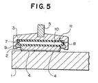
- the polishing apparatus is arranged such that a mount plate 2 is pressed downward by means of a hollow member 11 in which a fluid 10 is sealed by a barrier membrane 8. More specifically, in the polishing apparatus, the disc-shaped hollow member 11, in which the fluid 10 is sealed by the barrier membrane 8, is interposed between the mount plate 2 and a mount head 3, and the mount head 3 is fixed to a cylindrical pressurizing shaft 5.
- the hollow member 11 is fixed to the recess 7 of the mount head 3 by a retainer 9 with the upper surface of it in intimate contact with the inner flat surface of the recess 7.
- the hollow member 11 itself is composed of the barrier membrane 8 which is formed of an elastic material.
- the pressurizing shaft 5 is pressed downward. With this operation, the flat surface inside the mount head 3 presses the fluid 10 in the hollow member 11 through the barrier membrane 8. As a result, the fluid 10 is pressurized to thereby press the upper surface of the mount plate 2 through the barrier membrane 8.
- the hollow member 11, which is composed of the barrier membrane 8 and the inside of which is filled with the fluid 10, is fitted to the lower portion of the mount head 3; the outer periphery of the barrier membrane 8 is fixed to the mount head 3 by the ring-shaped retainer 9; the barrier membrane 8 is caused to come into intimate contact with the upper surface of the mount plate 2; and the upper surface of the mount plate 2 is pressed by pressure of the fluid 10.
- the barrier membrane 8 does not uniformly press the upper surface of the mount plate 2, when the silicon wafers 4 are polished with the polishing apparatus, there is a problem that the silicon wafers 4 cannot be uniformly polished.
- the barrier membrane 8 when the inside of the barrier membrane 8, which constitutes the hollow member 11, is filled with air, the barrier membrane 8 ordinarily expands like a balloon because the barrier membrane 8 itself is formed to have an approximately constant thickness. Thus, the upper surface of the mount plate 2 is not uniformly pressed by the barrier membrane 8.
- An object of the present invention is to provide a polishing apparatus capable of pressing the entire surface of a silicon wafer with an approximately constant force by causing a hollow member, which is filled with air in the inside thereof, to apply an approximately constant pressing force to the entire surface of a mount plate.
- Another object of the present invention is to provide a polishing apparatus capable of adjusting a force for pressing the silicon wafer by adjusting the pressing force applied to the amount plate.
- the present invention employs a polishing apparatus for polishing the lower surface of a workpiece in the state that a mount plate having the workpiece fixed to the lower surface thereof is pressed against a surface plate located under the mount plate by a mount head disposed above the mount plate, the polishing apparatus comprising a hollow member disposed in the mount head, the hollow member having a fluid sealed therein and a cross section in which a wall thickness is formed larger on the lower side thereof, wherein the hollow member approximately uniformly presses the mount plate through the portion thereof which is in contact with the mount plate.
- a press plate for pressing the hollow member and an adjustment member are disposed in the mount head, the adjustment member can be displaced with respect to the press plate, and the hollow member is adjusted by the adjustment member so that the mount plate can be approximately uniformly pressed by the entire surface of the hollow member which is in contact with the mount plate.
- the adjustment member can be adjusted by air pressure.
- the present invention employs a polishing apparatus for polishing the lower surface of a workpiece in the state that a mount plate having the workpiece fixed to the lower surface thereof is pressed against a surface plate located under the mount plate by a mount head disposed above the mount plate, the polishing apparatus comprising a hollow member disposed in the mount head, the hollow member having a fluid sealed therein and a cross section in which a wall thickness is formed larger on the lower side thereof; a press plate and an adjustment member disposed in the mount head, the press plate being abutted against the hollow member; and a spring member for pressing the press plate, wherein the hollow member is pressed by the press plate so as to press the mount plate in a prescribed pressed state, the adjustment member is adjusted so that the portion of the hollow member, which is abutted against the mount plate, presses the mount plate approximately uniformly, and the press force is changed by the spring member while the mount plate is uniformly pressed.
- the adjustment member can be adjusted by air pressure.
- the mount plate for pressing a silicon wafer is uniformly pressed by the hollow member with the arrangements as described above, the silicon wafer is uniformly pressed.
- the adjustment member since the hollow member can be partly pressed by the adjustment member, the adjustment member permits the respective portions of the hollow member to uniformly press the mount plate, whereby an approximately uniform press force can be applied to the respective portions of the silicon wafer. Further, when the pressure in the hollow member is changed due to aged deterioration, an optimum press force can be applied in the state that a uniform press force is maintained to the silicon wafer by pressing the entire hollow member by the press plate.
- FIG. 1 An embodiment of a polishing apparatus of the present invention is shown in FIG. 1, wherein numerals 1 and 2 denote a surface plate and a mount plate, respectively which are similar to those used in the conventional polishing apparatus.
- the mount plate 2 is placed on the upper surface of the surface plate 1 in the state that silicon wafers 4 are fixed to the lower surface of it.
- a hollow shaft member 20 is disposed above the mount plate 2, and a mount head 3, which has an open lower surface, is mounted on the hollow shaft member 20 continuously to the lower end thereof.
- a second hollow support member 22 is disposed to the upper surface of the press plate 21 so as to pass through the upper portion of the mount head 3.
- a first support member 23 which extends into the shaft member 20 from an upper side, is rotatably coupled with the second support member 22 through a bearing 24.
- the first support member 23 is coupled with the second support member 22 through the bearing 24 in the state that the upper end of it is elastically pressed downward by a spring member 25.
- the second support member 22 can be elastically displaced upward and downward together with the first support member 23 as well as rotated with respect to the first support member 23.
- the thickness of the barrier membrane 8 is not uniform. More specifically, the thickness of the barrier membrane 8 is larger on the upper side of it than the lower side thereof, that is, the barrier membrane 8 has a larger wall thickness on the side of it which is abutted against the mount plate 2.
- the wall thickness of the barrier membrane 8 is changed so that the contact surface thereof is made flat similarly to the arrangement of a radial tire.
- FIG. 2 is a schematic sectional view explaining the hollow member 11.
- the wall thickness of the barrier membrane 8 is formed larger on the lower side of it than on the upper side and both the sides thereof. Furthermore, the wall thicknesses of the boundaries 28 and 29, which are located between both the sides and the lower side, are changed so that they are not deformed when they come into contact with the mount plate 2.
- abrasive grain such as an alkaline suspension of colloidal silica, or the like is dispersed on the upper surface of the surface plate 1. Thereafter, the respective components are disposed to the polishing apparatus as shown in FIG. 1.
- the silicon wafers 4 are pressed against the upper surface of the surface plate 1 at desired pressure through the mount plate 2 by pressing the press plate 21, which is abutted against the upper surface of the hollow member 11 disposed in the mount head 3 located at the lower portion of the shaft member 20, in the state that the shaft member 20 is fixed.
- the hollow member 11 is arranged such that the wall thickness of the barrier membrane 8 is made larger on the lower side of it than on the upper side thereof.
- the wall thicknesses of the boundaries 28 and 29, which are located between both the sides and the lower side, are changed so that they are not deformed when they come into contact with the mount plate 2. Accordingly, the hollow member 11 is deformed similarly to the radial tire and comes into contact with the mount plate 2 at an approximately uniform press force.
- a cutout 26 is formed to the press plate 21 by partly cutting out it and an adjustment member 27, which is butted against the upper surface of the hollow member 11, is disposed in the cutout 26.
- an adjustment member 27, which is butted against the upper surface of the hollow member 11, is disposed in the cutout 26.
- the swelling state of the hollow member 11 can be adjusted by changing the state in which the adjustment member 27 is pressed against the hollow member 11.
- the adjustment of the hollow member 11 and the structure of the lower side of the hollow member 11, which is arranged similarly to that of the radial tire, permit the mount plate 2 to be pressed at substantially the same pressure at any portions thereof.
- the adjustment member 27 can be displaced by air pressure.
- the hollow member 11, in which the fluid 10 is sealed applies an approximately constant press force to the entire surface of the mount plate 2 so that the entire surfaces of the silicon wafers 4 can be pressed at an approximately constant press force.
- the hollow member 11 presses the upper surface of the mount plate 2, whereby the silicon wafers 4, which are fixed to the lower surface of the mount plate 2, are pressed against the upper surface of the surface plate 1.
- the mount plate 2 is rotated in the same direction as that of the surface plate 1 in the same manner in the conventional polishing apparatus to thereby polish the lower surfaces of the silicon wafers 4.
- the polishing apparatus of the present invention since the portion of the mount plate 2 which is in contact with the hollow member 11 receives the approximately uniform press force from the hollow member 11, the polished surfaces of the silicon wafers 4 are not deformed.
- the silicon wafers 4 are approximately uniformly pressed against the upper surface of the surface plate 1, there is not a possibility that the silicon wafers 4 are irregularly polished.
- the respective portions of the hollow member 11, which are in contact with the mount plate 2 can be provided with an approximately uniform press force by the arrangement of the hollow member 11 itself and the adjustment member 27 which partly presses the hollow member 11. Accordingly, the silicon wafers 4 are approximately uniformly pressed to thereby prevent the silicon wafers 4 from being irregularly polished.
- the press force can be also changed while maintaining the silicon wafers in an approximately uniformly pressed state, the press force applied to the silicon wafers can be easily adjusted.
- the portion of the mount plate, where the hollow member is in contact with it can be approximately uniformly pressed.
- the mount plate thereby presses the silicon wafers against the surface plate approximately uniformly so that the silicon wafers can be uniformly polished without irregularity.
- the lower surface of the hollow member and the portions thereof located on both the sides of the lower surface can be adjusted so that they approximately uniformly press the mount plate as well as an optimum pressed state can be obtained.
- the silicon wafers can be reliably prevented from being irregularly polished.
- the hollow member can be pressed by the press plate while maintaining the uniformly pressed state of the mount plate, the press force can be easily increased or reduced, whereby there can be obtained an effect that the press force is adjustable.
Landscapes
- Engineering & Computer Science (AREA)
- Mechanical Engineering (AREA)
- Finish Polishing, Edge Sharpening, And Grinding By Specific Grinding Devices (AREA)
- Mechanical Treatment Of Semiconductor (AREA)
Applications Claiming Priority (2)
| Application Number | Priority Date | Filing Date | Title |
|---|---|---|---|
| JP18440598 | 1998-06-30 | ||
| JP18440598A JP2000015558A (ja) | 1998-06-30 | 1998-06-30 | 研磨装置 |
Publications (2)
| Publication Number | Publication Date |
|---|---|
| EP0976497A2 true EP0976497A2 (de) | 2000-02-02 |
| EP0976497A3 EP0976497A3 (de) | 2003-01-15 |
Family
ID=16152602
Family Applications (1)
| Application Number | Title | Priority Date | Filing Date |
|---|---|---|---|
| EP99112008A Withdrawn EP0976497A3 (de) | 1998-06-30 | 1999-06-21 | Poliervorrichtung |
Country Status (4)
| Country | Link |
|---|---|
| EP (1) | EP0976497A3 (de) |
| JP (1) | JP2000015558A (de) |
| KR (1) | KR20000006474A (de) |
| TW (1) | TW402546B (de) |
Cited By (1)
| Publication number | Priority date | Publication date | Assignee | Title |
|---|---|---|---|---|
| TWI462784B (zh) * | 2008-09-05 | 2014-12-01 | Hon Hai Prec Ind Co Ltd | 清洗裝置 |
Families Citing this family (2)
| Publication number | Priority date | Publication date | Assignee | Title |
|---|---|---|---|---|
| CN110142686B (zh) * | 2019-06-18 | 2023-08-15 | 肇庆金马领科智能科技有限公司 | 防尘恒力装置及控制方法、机械臂、研磨设备及机器人 |
| CN113070802B (zh) * | 2021-04-06 | 2022-03-11 | 安徽禾臣新材料有限公司 | 一种用于半导体抛光加工的无蜡垫及生产方法 |
Family Cites Families (4)
| Publication number | Priority date | Publication date | Assignee | Title |
|---|---|---|---|---|
| US5643053A (en) * | 1993-12-27 | 1997-07-01 | Applied Materials, Inc. | Chemical mechanical polishing apparatus with improved polishing control |
| US5643061A (en) * | 1995-07-20 | 1997-07-01 | Integrated Process Equipment Corporation | Pneumatic polishing head for CMP apparatus |
| JP3566430B2 (ja) * | 1995-12-20 | 2004-09-15 | 株式会社ルネサステクノロジ | 半導体装置の製造方法 |
| JP3106418B2 (ja) * | 1996-07-30 | 2000-11-06 | 株式会社東京精密 | 研磨装置 |
-
1998
- 1998-06-30 JP JP18440598A patent/JP2000015558A/ja active Pending
-
1999
- 1999-06-16 TW TW088110115A patent/TW402546B/zh not_active IP Right Cessation
- 1999-06-21 EP EP99112008A patent/EP0976497A3/de not_active Withdrawn
- 1999-06-25 KR KR1019990024271A patent/KR20000006474A/ko not_active Withdrawn
Cited By (1)
| Publication number | Priority date | Publication date | Assignee | Title |
|---|---|---|---|---|
| TWI462784B (zh) * | 2008-09-05 | 2014-12-01 | Hon Hai Prec Ind Co Ltd | 清洗裝置 |
Also Published As
| Publication number | Publication date |
|---|---|
| JP2000015558A (ja) | 2000-01-18 |
| TW402546B (en) | 2000-08-21 |
| EP0976497A3 (de) | 2003-01-15 |
| KR20000006474A (ko) | 2000-01-25 |
Similar Documents
| Publication | Publication Date | Title |
|---|---|---|
| US4194324A (en) | Semiconductor wafer polishing machine and wafer carrier therefor | |
| KR910009320B1 (ko) | 연마장치 | |
| US5193316A (en) | Semiconductor wafer polishing using a hydrostatic medium | |
| US5980367A (en) | Semiconductor wafer polishing machine and method | |
| JP5216542B2 (ja) | 化学機械研磨ヘッド用保持リング | |
| US7897007B2 (en) | Substrate holding apparatus and substrate polishing apparatus | |
| US5643061A (en) | Pneumatic polishing head for CMP apparatus | |
| US7108592B2 (en) | Substrate holding apparatus and polishing apparatus | |
| JP3106418B2 (ja) | 研磨装置 | |
| US5885135A (en) | CMP wafer carrier for preferential polishing of a wafer | |
| EP1101566B1 (de) | Werkstückhalter und Poliervorrichtung mit demselben | |
| US20070212988A1 (en) | Polishing apparatus | |
| JP2001135602A (ja) | 圧力伝達機構を有するキャリヤヘッド | |
| JP2001038604A (ja) | 可撓膜及びエッジロードリングを有するキャリヤヘッド | |
| JP2011522416A (ja) | 半導体ウェハの研磨装置及び研磨方法 | |
| US20030181151A1 (en) | Carrier head with a vibration reduction feature for a chemical mechanical polishing system | |
| US6273794B1 (en) | Apparatus and method for grinding a semiconductor wafer surface | |
| US6848980B2 (en) | Vibration damping in a carrier head | |
| KR20040023228A (ko) | 화학적 기계적 평탄화 기계의 폴리싱 헤드 | |
| US6641461B2 (en) | Chemical mechanical polishing apparatus having edge, center and annular zone control of material removal | |
| JP2504420B2 (ja) | 研磨装置 | |
| KR20010024166A (ko) | 웨이퍼 공정 장치 | |
| KR100419135B1 (ko) | 직접 공기 웨이퍼 연마 압력 장치를 구비한 헤드를 이용한화학적 기계적 연마용 장치 및 방법 | |
| JP2000015558A (ja) | 研磨装置 | |
| TW200403737A (en) | Vibration damping in a carrier head |
Legal Events
| Date | Code | Title | Description |
|---|---|---|---|
| PUAI | Public reference made under article 153(3) epc to a published international application that has entered the european phase |
Free format text: ORIGINAL CODE: 0009012 |
|
| 17P | Request for examination filed |
Effective date: 19990621 |
|
| AK | Designated contracting states |
Kind code of ref document: A2 Designated state(s): AT BE CH CY DE DK ES FI FR GB GR IE IT LI LU MC NL PT SE |
|
| AX | Request for extension of the european patent |
Free format text: AL;LT;LV;MK;RO;SI |
|
| PUAL | Search report despatched |
Free format text: ORIGINAL CODE: 0009013 |
|
| AK | Designated contracting states |
Kind code of ref document: A3 Designated state(s): AT BE CH CY DE DK ES FI FR GB GR IE IT LI LU MC NL PT SE |
|
| AX | Request for extension of the european patent |
Free format text: AL;LT;LV;MK;RO;SI |
|
| RIC1 | Information provided on ipc code assigned before grant |
Free format text: 7B 24B 37/04 A, 7H 01L 21/304 B |
|
| RTI1 | Title (correction) |
Free format text: POLISHING APPARATUS |
|
| STAA | Information on the status of an ep patent application or granted ep patent |
Free format text: STATUS: THE APPLICATION IS DEEMED TO BE WITHDRAWN |
|
| 18D | Application deemed to be withdrawn |
Effective date: 20030103 |