EP0977105A1 - Regler mit Strombegrenzungsfunktion und Verfahren dazu - Google Patents
Regler mit Strombegrenzungsfunktion und Verfahren dazu Download PDFInfo
- Publication number
- EP0977105A1 EP0977105A1 EP98114383A EP98114383A EP0977105A1 EP 0977105 A1 EP0977105 A1 EP 0977105A1 EP 98114383 A EP98114383 A EP 98114383A EP 98114383 A EP98114383 A EP 98114383A EP 0977105 A1 EP0977105 A1 EP 0977105A1
- Authority
- EP
- European Patent Office
- Prior art keywords
- transistor
- current
- output
- voltage
- magnitude
- Prior art date
- Legal status (The legal status is an assumption and is not a legal conclusion. Google has not performed a legal analysis and makes no representation as to the accuracy of the status listed.)
- Withdrawn
Links
Images

Classifications
-
- G—PHYSICS
- G05—CONTROLLING; REGULATING
- G05F—SYSTEMS FOR REGULATING ELECTRIC OR MAGNETIC VARIABLES
- G05F3/00—Non-retroactive systems for regulating electric variables by using an uncontrolled element, or an uncontrolled combination of elements, such element or such combination having self-regulating properties
- G05F3/02—Regulating voltage or current
- G05F3/08—Regulating voltage or current wherein the variable is DC
- G05F3/10—Regulating voltage or current wherein the variable is DC using uncontrolled devices with non-linear characteristics
- G05F3/16—Regulating voltage or current wherein the variable is DC using uncontrolled devices with non-linear characteristics being semiconductor devices
- G05F3/20—Regulating voltage or current wherein the variable is DC using uncontrolled devices with non-linear characteristics being semiconductor devices using diode- transistor combinations
- G05F3/22—Regulating voltage or current wherein the variable is DC using uncontrolled devices with non-linear characteristics being semiconductor devices using diode- transistor combinations wherein the transistors are of the bipolar type only
- G05F3/222—Regulating voltage or current wherein the variable is DC using uncontrolled devices with non-linear characteristics being semiconductor devices using diode- transistor combinations wherein the transistors are of the bipolar type only with compensation for device parameters, e.g. Early effect, gain, manufacturing process, or external variations, e.g. temperature, loading, supply voltage
- G05F3/225—Regulating voltage or current wherein the variable is DC using uncontrolled devices with non-linear characteristics being semiconductor devices using diode- transistor combinations wherein the transistors are of the bipolar type only with compensation for device parameters, e.g. Early effect, gain, manufacturing process, or external variations, e.g. temperature, loading, supply voltage producing a current or voltage as a predetermined function of the temperature
Definitions
- the present invention generally relates to electronic circuits, and, more particularly, to regulators, and relates to a method for regulating.
- a voltage regulator provides a substantially temperature independent output voltage V OUT to a consuming circuit ( "consumer circuit"). It is often required that the regulator has a current limiting function which substantially reduces or cuts off output current I OUT when I OUT reaches a maximum allowable current I OUT MAX .
- the current limiting function should not interfere with the normal operation of the regulator when (I OUT ⁇ I OUT MAX ).
- the time between reaching I OUT MAX and reducing (and/or cutting off) I OUT is the response time T RESP and should be short enough to prevent damages in the current regulator and in the consumer circuit.
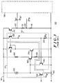
- FIG. 1 illustrates a simplified circuit diagram of prior art regulator 100.
- Regulator 100 supplies power (output voltage V OUT ', output current I OUT ) to consumer circuit 199 (illustrated dashed).
- Regulator 100 comprises output transistor 110, feedback resistors 115 and 116, current limiting portion 101 (dashed frame, with transistor 120, resistor 130 and transistor 140), and driver portion 111 (dashed frame, with transistors 150, 160, 170 and 180, current source 155, and resistors 165 and 166).
- transistor 120 in current limiting portion 101 has an effective emitter area which is the 1 / N fraction of the emitter area of output transistor 110.
- Output transistor 110 has an emitter coupled to reference line 191 and a collector coupled to output node 105.
- Output node 105 is coupled to reference line 192 via resistors 115 and 116.
- transistor 180 is coupled in a current mirror arrangement to transistor 110.
- Transistor 180 has an emitter coupled to reference line 191 and a base and a collector coupled together to the base of transistor 110.
- the collector of transistor 180 is coupled to a collector of transistor 170.
- An emitter of transistor 170 is coupled to reference line 192.
- Transistor 160 has a collector coupled to reference line 191 via resistor 165 and has an emitter coupled to reference line 192 via resistor 166.
- the emitter of transistor 160 is coupled to a base of transistor 170.
- Current source 155 is coupled between reference line 191 and an emitter of transistor 150.
- the emitter of transistor 150 is also coupled to the base of transistor 160.
- a collector of transistor 150 is coupled to reference line 192.
- Transistor 150 receives control signal V IN ' at a base.
- transistor 120 has a base coupled to the base of transistor 110, an emitter coupled to reference line 191 and a collector coupled via resistor 130 to reference line 192 (current I CL ').
- a base-emitter path of transistor 140 is coupled in parallel to resistor 130 (between the collector of transistor 120 and reference line 191).
- a collector of transistor 140 is coupled to the base of transistor 160 of driver portion 111.
- Output transistor 110 provides output current I OUT ' on node 105 depending on control signal V IN which is propagated by driver portion 111.
- the feedback signal V FB at node 106 between resistors 115 and 116 can be feed back to control signal V IN '.
- the feedback circuit is not illustrated.
- Resistor 130 value R CL '
- V CL ' V CL ' * R CL '
- V BE START ' V BE START ' (e.g., 0.6 volts) at which transistor 140 becomes conductive. This keeps the driving capacity of driver portion 111 at a predetermined minimum. With driver portion 111 in such a state, transistor 110 substantially limits output current I OUT '.
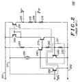
- FIG. 2 illustrates a simplified circuit diagram of further prior art regulator 200.
- Regulator 200 comprises output transistor 210, output resistors 215 and 216, current limiting portion 201 (dashed frame, with resistor 230 and transistor 240), and driver portion 211 (dashed frame, with transistors 250, 260 and 270, current source 255, and resistors 265 and 266).
- the components of regulator 200 are coupled similarly as in regulator 100 of FIG. 1.
- reference numbers 105/205, 106/206, 110/210, 115/215, 116/216, 101/201, 111/211, 130/230, 140/240, 150/250, 155/255, 160/260, 165/265, 166/266, 170/270, 180/280, 191/291, and 192/292 refer to analogous components. However, their function can be different as described in the following.
- Output transistor 210 and transistor 280 form a current mirror.
- Auxiliary current I CL '' is substantially equal to the base current of output transistor 110 (or to a scaled base current).
- resistor 230 value R CL ''
- V CL '' V CL '' * R CL ''
- Transistor 140 keeps driver portion 211 at a predetermined driving capacity and transistor 210 substantially limits output current I OUT ''.
- Regulator 200 consumes a smaller total current than regulator 100 (see transistor 120). But the other mentioned disadvantages remain the same.
- the present invention seeks to provide regulators with current limiting function which mitigate or avoid these and other disadvantages and limitations of the prior art.
- FIGS. 3-4 Embodiments of a regulator with current limiting function of the present invention are explained in connection with FIGS. 3-4.
- the figures and the description refer to bipolar transistors. Persons of skill in the art are able, based on the description herein, to implement the present invention with other technologies, such as CMOS or others.
- transistor is intended to include any device or arrangement having at least two main electrodes (e.g., emitters and collectors) and a control electrode (e.g., a base). The impedance between the main electrodes is controlled by a signal applied to the control electrode.
- the transistors are classified into npn-transistors and pnp-transistors. This is convenient for the embodiments of the present invention, but not essential. Persons of skill in the art are able, based on the description herein, to use transistor types in other combinations without departing from the scope of the invention.
- Signals are conveniently introduced as voltages (e.g., V IN , V REF ) or currents (I B , I CL ) as they appear in the embodiments.
- V IN voltage
- V REF voltage
- I B current
- I CL currents
- the present invention has a number of advantages over the prior art, such as: (a) less temperature dependency, (b) shorter response time T RESP , and (c) higher stability for high output currents (I OUT ⁇ I OUT MAX ) due to lower feedback gain.
- FIG. 3 illustrates a simplified circuit diagram of regulator 300 according to a first embodiment of the present invention.
- Regulator 300 has reference line 391 (e.g., voltage V CC ), reference line 392 (e.g., ground “GND” at around zero volts), control terminal 394 (control signal V IN ), reference terminal 393 (reference signal V REF ), and feedback node 306 (feedback signal V FB ).
- Regulator 300 comprises output transistor 310, input transistor 350, clamp transistor 352, chain transistors 360 and 370, mirror transistor 380, resistors 315, 316, 330, 365, 366, and current source 355.
- V CC voltage V CC
- reference line 392 e.g., ground “GND” at around zero volts
- control terminal 394 control signal V IN
- reference terminal 393 reference terminal 393
- feedback node 306 feedback node 306
- Regulator 300 comprises output transistor 310, input transistor 350, clamp transistor 352, chain transistors 360 and
- transistors 310, 350, 352 and 380 are pnp-transistors, and transistors 360 and 370 are npn-transistors. As mentioned above, the transistor types are not important. Having chain transistors 360 and 370 of the same type (e.g., npn) is convenient. Transistors 350, 360, 370, and 380, current source 355, and resistors 365 and 366 form driver portion 311 (dashed frame). Transistors 360 and 370 are preferably arranged as emitter followers and form chain 335 ("arrangement", dashed frame). Resistor 330 and clamp transistor 352 in connection with other components in driver portion 311 provide the current limiting function. Unlike as in the prior art examples of FIGS.
- Regulator 300 receives input current I CC at reference line 391. Regulator provides power (output voltage V OUT , output current I OUT ) at output node 305 to a consumer circuit (not illustrated in FIG. 3, cf. circuit 199 in FIG. 1).
- an optional operational amplifier (not illustrated) can have inputs at feedback node 306 and at reference terminal 393 and an output at control terminal 394.
- Output transistor 310 has an emitter coupled to reference line 391 and a collector coupled to output node 305.
- Resistors 315 and 316 are serially coupled between output node 305 and reference line 392 via feedback node 306 (voltage sensor arrangement).
- Output transistor 310 and mirror transistor 380 have their bases coupled together to a collector of transistor 380 and have emitters coupled to reference line 391 to form a current mirror.
- a collector of transistor 380 is coupled to a collector of chain transistor 370.
- An emitter of transistor 370 is coupled reference line 392 via resistor 330.
- Transistor 360 has a collector coupled to reference line 391 via resistor 365, and has an emitter coupled to reference line 392 via resistor 366.
- the emitter of transistor 360 is also coupled to a base of transistor 370.
- Current source 355 is coupled between reference line 391 and intermediate node 351.
- Intermediate node 351 is coupled to a base of transistor 360, to an emitter of clamp transistor 352 and to an emitter of input transistor 350.
- a collector of input transistor 350 is coupled to reference line 392.
- a base of input transistor 350 is coupled to control terminal 394.
- a collector of clamp transistor 352 is coupled to reference terminal 392.
- a base of clamp transistor 352 is coupled to reference terminal 393.
- input transistor 350 and clamp transistor 352 have their main electrodes couple in parallel between intermediate node 351 and reference line 392.
- Input current I CC is the current going into regulator 300 at reference terminal 391.
- Output current I OUT is the collector current of output transistor 310 wherein the current through resistors 315 and 316 is neglected.
- Control current I B is the base current of output transistor 310 and flow from the base of transistor 310 to reference terminal 392.
- the base current is substantially proportional to the collector current ( ⁇ -relation known in the art).
- R CL is the Ohmic resistance value of resistor 330.
- V BE3 is the base-emitter voltage of chain transistor 370
- V BE2 is the base-emitter voltage of chain transistor 360
- V BE1 is the base emitter voltage of input transistor 350.
- Control signal V IN is defined as the voltage between control terminal 394 and reference line 392 across the base-collector path of input transistor 350
- reference voltage V REF is defined as the voltage between reference terminal 393 and reference line 392 across the base-collector path of clamp transistor 352.
- Feedback signal V FB is the voltage between feedback node 306 and reference line 392 across resistor 316.
- Current I Q is the current of current source 355 and is, preferably, a constant current.
- Node voltage V X is the voltage between intermediate node 351 and reference terminal 392.
- the current limiting function in regulator 300 is achieved by the operation of regulator 300 as follows: Output transistor 310 receives input voltage V CC at the emitter and provides output voltage V OUT at the collector (also current I CC and I OUT , respectively). Driver portion 311 controls transistor 310 through the base current I B . Resistor 330 carries current I CL (substantially proportional to I OUT ,I B , explained above) and provides voltage drop V CL . Chain 335 forwards voltage drop V CL to node 351. When I OUT increases, then voltage V X at node 351 also increases. Optionally, input transistor 350 receives V IN and controls the base current I B through chain 335. Transistor 352 clamps the voltage V X at node 351 to V XMAX (V X ⁇ V X MAX ). This affects also the maximum magnitude of V CL and therefore limits I OUT to I OUT MAX .
- Voltage changes due to temperature variations are partly compensated.
- Voltage V CL across resistor 330 has a positive temperature coefficient ("temp co").
- chain 335 provides a pn-junction voltage (V CL - V IN ) with a negative temp co which compensates the positive temp co of voltage drop V CL .
- Persons of skill in the art are able, based on the description herein, to replace transistors 360 and 370 by other semiconductor devices whose pn-junctions provide similar voltages.
- reference voltage V REF is substantially independent from the temperature. This is convenient, but not necessary. It is possible to apply a V REF which substantially does depend on the temperature. In such a case, the temperature dependency of the current limiting portion can be arbitrarily adjusted as required by, for example, the consumer circuit.
- the response time T RESP is shorter than in prior art solutions. This is an important advantage of the present invention. As mentioned above, regulator 300 has a better stability due to lower feedback gain and higher stability for high output currents (I OUT ⁇ I OUT MAX ).
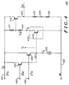
- FIG. 4 illustrates a simplified circuit diagram of regulator 400 according to a second embodiment of the present invention.
- reference numbers 300/400, 305/405, 306/406, 310/410, 315/415, 316/416, 330/430, 352/452, 350/450, 335/435, 370/470, 391/491, 392/492, 393/493 and 394/494 refer to analogous components. However, their function can be different as described in the following.
- the analogous components are: output transistor 410 (e.g., pnp-type), input transistor 450 (e.g., npn-type), clamp transistor 452 (e.g., npn-type), chain transistor 470 (forming chain 435, e.g., pnp-type, dashed), resistors 415, 416 and 430, and current source 455.
- Regulator 400 further comprises resistor 431.
- Output transistor 410 has an emitter coupled to reference line 491 and a collector coupled to output node 405.
- a base of transistor 410 is coupled to reference line 491 via resistor 431 and is coupled to an emitter of transistor 470 via resistor 430.
- Output node 405 is coupled to reference line 492 via resistor 415, feedback node 406, and resistor 416 (voltage sensor).
- Chain transistor 470 has a collector coupled to reference line 492 and a base coupled to intermediate node 451 (base-emitter voltage V BE3 ).
- Input transistor 450 has a collector coupled to reference line 491, an emitter coupled to intermediate node 451, and a base coupled to input terminal 494.
- Clamp transistor 452 has a collector coupled to reference line 491, an emitter coupled to intermediate node 451, and a base coupled to reference terminal 493.
- Current source is coupled between intermediate node 451 and reference line 492.
- Resistor current I CL through resistor 430 is, preferably, proportionally related to the control current I B (base current) of output transistor 410.
- Voltage V X is referred to reference line 491 (different from FIG. 3).
- regulator 300/400 with a current limiting function which comprises: (a) output transistor 310/410 having an emitter to receive input voltage V CC (on line 391/491), a collector to provide output current I OUT , and a base to receive control current I B (base current); (b) resistor 330/430 which carries resistor current I CL proportional to control current I B at the base of transistor 310/410 and which provides voltage drop V CL ; (c) chain 335/435 to forward voltage drop V CL to intermediate node 351/451, such that an increase of I OUT leads to an increase of node voltage V X between intermediate node 351/451 and reference line 392/491; (d) input transistor 350/450 having an emitter coupled to intermediate node 351/451, a collector coupled reference line 392/491, and a base to receive control signal V IN , input transistor 350/450 controlling output transistor 310/410 (e.g., via transistors 360,
- clamp transistor 352/452 having an emitter coupled to intermediate node 351/451, a collector coupled to reference line 392/491, and a base to receive reference signal V REF , such that node voltage V X is limited ("clamped") when output current I OUT increases to predetermined magnitude I OUT MAX , and that input transistor 350/450 prevents I OUT from increasing beyond I OUT MAX .
- circuit 300 having output transistor 310 to transfer an input 391 to an output 305 wherein output current I OUT is limited.
- Circuit 300 is characterized by features (a) and (b) :
- Regulator 300/400 has output transistor 310/410 that receives a first current (e.g., I CC ) at a first main electrode (e.g., emitter) and a second current (e.g., I B ) at a control electrode (e.g., base).
- Output transistor 310/410 provides a third current (e.g., output current I OUT ) at a second main electrode (e.g., collector).
- the third current is limited to predetermined maximum current (e.g., I OUT MAX ) by the following steps:
Landscapes
- Engineering & Computer Science (AREA)
- Microelectronics & Electronic Packaging (AREA)
- Physics & Mathematics (AREA)
- Nonlinear Science (AREA)
- Electromagnetism (AREA)
- General Physics & Mathematics (AREA)
- Radar, Positioning & Navigation (AREA)
- Automation & Control Theory (AREA)
- Continuous-Control Power Sources That Use Transistors (AREA)
Priority Applications (1)
| Application Number | Priority Date | Filing Date | Title |
|---|---|---|---|
| EP98114383A EP0977105A1 (de) | 1998-07-31 | 1998-07-31 | Regler mit Strombegrenzungsfunktion und Verfahren dazu |
Applications Claiming Priority (1)
| Application Number | Priority Date | Filing Date | Title |
|---|---|---|---|
| EP98114383A EP0977105A1 (de) | 1998-07-31 | 1998-07-31 | Regler mit Strombegrenzungsfunktion und Verfahren dazu |
Publications (1)
| Publication Number | Publication Date |
|---|---|
| EP0977105A1 true EP0977105A1 (de) | 2000-02-02 |
Family
ID=8232381
Family Applications (1)
| Application Number | Title | Priority Date | Filing Date |
|---|---|---|---|
| EP98114383A Withdrawn EP0977105A1 (de) | 1998-07-31 | 1998-07-31 | Regler mit Strombegrenzungsfunktion und Verfahren dazu |
Country Status (1)
| Country | Link |
|---|---|
| EP (1) | EP0977105A1 (de) |
Citations (5)
| Publication number | Priority date | Publication date | Assignee | Title |
|---|---|---|---|---|
| US4914317A (en) * | 1988-12-12 | 1990-04-03 | Texas Instruments Incorporated | Adjustable current limiting scheme for driver circuits |
| DE4300592A1 (de) * | 1993-01-13 | 1994-07-14 | Telefunken Microelectron | Anordnung zur Begrenzung eines Ausgangsstroms |
| US5550462A (en) * | 1993-06-29 | 1996-08-27 | Sharp Kabushiki Kaisha | Regulated power supply circuit and an emitter follower output current limiting circuit |
| EP0735452A2 (de) * | 1995-03-28 | 1996-10-02 | STMicroelectronics, Inc. | Strombegrenzungsschaltung |
| US5644217A (en) * | 1995-04-20 | 1997-07-01 | Rohm Co., Ltd. | Emitter coupled logic output circuit |
-
1998
- 1998-07-31 EP EP98114383A patent/EP0977105A1/de not_active Withdrawn
Patent Citations (5)
| Publication number | Priority date | Publication date | Assignee | Title |
|---|---|---|---|---|
| US4914317A (en) * | 1988-12-12 | 1990-04-03 | Texas Instruments Incorporated | Adjustable current limiting scheme for driver circuits |
| DE4300592A1 (de) * | 1993-01-13 | 1994-07-14 | Telefunken Microelectron | Anordnung zur Begrenzung eines Ausgangsstroms |
| US5550462A (en) * | 1993-06-29 | 1996-08-27 | Sharp Kabushiki Kaisha | Regulated power supply circuit and an emitter follower output current limiting circuit |
| EP0735452A2 (de) * | 1995-03-28 | 1996-10-02 | STMicroelectronics, Inc. | Strombegrenzungsschaltung |
| US5644217A (en) * | 1995-04-20 | 1997-07-01 | Rohm Co., Ltd. | Emitter coupled logic output circuit |
Similar Documents
| Publication | Publication Date | Title |
|---|---|---|
| US6222357B1 (en) | Current output circuit with controlled holdover capacitors | |
| EP0826167B1 (de) | Stromkreisvorrichtung zum liefern eines gleichstromes | |
| US7151365B2 (en) | Constant voltage generator and electronic equipment using the same | |
| KR100547236B1 (ko) | 전력증폭기에서의 바이어스 안정화 회로 | |
| US6249162B1 (en) | Hysteresis circuit | |
| EP0516848B1 (de) | Schaltung zur verhinderung der sättigung eines transistors | |
| KR920009548B1 (ko) | 전류원 장치 | |
| US5808507A (en) | Temperature compensated reference voltage source | |
| JP4083573B2 (ja) | 高周波増幅装置 | |
| US20030038679A1 (en) | Circuit configuration for setting the operating point of a radiofrequency transistor and amplifier circuit | |
| US6285258B1 (en) | Offset voltage trimming circuit | |
| EP0977105A1 (de) | Regler mit Strombegrenzungsfunktion und Verfahren dazu | |
| US6175265B1 (en) | Current supply circuit and bias voltage circuit | |
| US4851759A (en) | Unity-gain current-limiting circuit | |
| US5617056A (en) | Base current compensation circuit | |
| EP0110720B1 (de) | Stromspiegelschaltungsanordnung | |
| JPH05175747A (ja) | 高出力fet増幅器 | |
| EP0611105B1 (de) | Stromquelle | |
| US6396319B2 (en) | Semiconductor integrated circuit with quick charging/discharging circuit | |
| EP0913930B1 (de) | Symmetrische transformatorlose Verstärkerschaltung | |
| JP3092062B2 (ja) | 半導体装置 | |
| EP0410764A2 (de) | Komparatorschaltung | |
| JP3105716B2 (ja) | カレントミラー回路 | |
| JPS6333390B2 (de) | ||
| JP3009980B2 (ja) | 可変利得増幅器 |
Legal Events
| Date | Code | Title | Description |
|---|---|---|---|
| PUAI | Public reference made under article 153(3) epc to a published international application that has entered the european phase |
Free format text: ORIGINAL CODE: 0009012 |
|
| AK | Designated contracting states |
Kind code of ref document: A1 Designated state(s): DE FR GB IT NL |
|
| AX | Request for extension of the european patent |
Free format text: AL;LT;LV;MK;RO;SI |
|
| 17P | Request for examination filed |
Effective date: 20000802 |
|
| AKX | Designation fees paid |
Free format text: DE FR GB IT NL |
|
| 17Q | First examination report despatched |
Effective date: 20000110 |
|
| STAA | Information on the status of an ep patent application or granted ep patent |
Free format text: STATUS: THE APPLICATION IS DEEMED TO BE WITHDRAWN |
|
| 18D | Application deemed to be withdrawn |
Effective date: 20010720 |