EP0977194A2 - Atomspeicher - Google Patents
Atomspeicher Download PDFInfo
- Publication number
- EP0977194A2 EP0977194A2 EP99110080A EP99110080A EP0977194A2 EP 0977194 A2 EP0977194 A2 EP 0977194A2 EP 99110080 A EP99110080 A EP 99110080A EP 99110080 A EP99110080 A EP 99110080A EP 0977194 A2 EP0977194 A2 EP 0977194A2
- Authority
- EP
- European Patent Office
- Prior art keywords
- read
- storage
- digital memory
- memory according
- interferometer
- Prior art date
- Legal status (The legal status is an assumption and is not a legal conclusion. Google has not performed a legal analysis and makes no representation as to the accuracy of the status listed.)
- Withdrawn
Links
Images

Classifications
-
- B—PERFORMING OPERATIONS; TRANSPORTING
- B82—NANOTECHNOLOGY
- B82Y—SPECIFIC USES OR APPLICATIONS OF NANOSTRUCTURES; MEASUREMENT OR ANALYSIS OF NANOSTRUCTURES; MANUFACTURE OR TREATMENT OF NANOSTRUCTURES
- B82Y10/00—Nanotechnology for information processing, storage or transmission, e.g. quantum computing or single electron logic
-
- G—PHYSICS
- G11—INFORMATION STORAGE
- G11B—INFORMATION STORAGE BASED ON RELATIVE MOVEMENT BETWEEN RECORD CARRIER AND TRANSDUCER
- G11B9/00—Recording or reproducing using a method not covered by one of the main groups G11B3/00 - G11B7/00; Record carriers therefor
-
- G—PHYSICS
- G11—INFORMATION STORAGE
- G11B—INFORMATION STORAGE BASED ON RELATIVE MOVEMENT BETWEEN RECORD CARRIER AND TRANSDUCER
- G11B9/00—Recording or reproducing using a method not covered by one of the main groups G11B3/00 - G11B7/00; Record carriers therefor
- G11B9/12—Recording or reproducing using a method not covered by one of the main groups G11B3/00 - G11B7/00; Record carriers therefor using near-field interactions; Record carriers therefor
- G11B9/14—Recording or reproducing using a method not covered by one of the main groups G11B3/00 - G11B7/00; Record carriers therefor using near-field interactions; Record carriers therefor using microscopic probe means, i.e. recording or reproducing by means directly associated with the tip of a microscopic electrical probe as used in Scanning Tunneling Microscopy [STM] or Atomic Force Microscopy [AFM] for inducing physical or electrical perturbations in a recording medium; Record carriers or media specially adapted for such transducing of information
- G11B9/1418—Disposition or mounting of heads or record carriers
-
- G—PHYSICS
- G11—INFORMATION STORAGE
- G11B—INFORMATION STORAGE BASED ON RELATIVE MOVEMENT BETWEEN RECORD CARRIER AND TRANSDUCER
- G11B9/00—Recording or reproducing using a method not covered by one of the main groups G11B3/00 - G11B7/00; Record carriers therefor
- G11B9/12—Recording or reproducing using a method not covered by one of the main groups G11B3/00 - G11B7/00; Record carriers therefor using near-field interactions; Record carriers therefor
- G11B9/14—Recording or reproducing using a method not covered by one of the main groups G11B3/00 - G11B7/00; Record carriers therefor using near-field interactions; Record carriers therefor using microscopic probe means, i.e. recording or reproducing by means directly associated with the tip of a microscopic electrical probe as used in Scanning Tunneling Microscopy [STM] or Atomic Force Microscopy [AFM] for inducing physical or electrical perturbations in a recording medium; Record carriers or media specially adapted for such transducing of information
- G11B9/1418—Disposition or mounting of heads or record carriers
- G11B9/1427—Disposition or mounting of heads or record carriers with provision for moving the heads or record carriers relatively to each other or for access to indexed parts without effectively imparting a relative movement
- G11B9/1436—Disposition or mounting of heads or record carriers with provision for moving the heads or record carriers relatively to each other or for access to indexed parts without effectively imparting a relative movement with provision for moving the heads or record carriers relatively to each other
-
- G—PHYSICS
- G11—INFORMATION STORAGE
- G11B—INFORMATION STORAGE BASED ON RELATIVE MOVEMENT BETWEEN RECORD CARRIER AND TRANSDUCER
- G11B9/00—Recording or reproducing using a method not covered by one of the main groups G11B3/00 - G11B7/00; Record carriers therefor
- G11B9/12—Recording or reproducing using a method not covered by one of the main groups G11B3/00 - G11B7/00; Record carriers therefor using near-field interactions; Record carriers therefor
- G11B9/14—Recording or reproducing using a method not covered by one of the main groups G11B3/00 - G11B7/00; Record carriers therefor using near-field interactions; Record carriers therefor using microscopic probe means, i.e. recording or reproducing by means directly associated with the tip of a microscopic electrical probe as used in Scanning Tunneling Microscopy [STM] or Atomic Force Microscopy [AFM] for inducing physical or electrical perturbations in a recording medium; Record carriers or media specially adapted for such transducing of information
- G11B9/1463—Record carriers for recording or reproduction involving the use of microscopic probe means
- G11B9/1472—Record carriers for recording or reproduction involving the use of microscopic probe means characterised by the form
-
- G—PHYSICS
- G11—INFORMATION STORAGE
- G11B—INFORMATION STORAGE BASED ON RELATIVE MOVEMENT BETWEEN RECORD CARRIER AND TRANSDUCER
- G11B9/00—Recording or reproducing using a method not covered by one of the main groups G11B3/00 - G11B7/00; Record carriers therefor
- G11B9/12—Recording or reproducing using a method not covered by one of the main groups G11B3/00 - G11B7/00; Record carriers therefor using near-field interactions; Record carriers therefor
- G11B9/14—Recording or reproducing using a method not covered by one of the main groups G11B3/00 - G11B7/00; Record carriers therefor using near-field interactions; Record carriers therefor using microscopic probe means, i.e. recording or reproducing by means directly associated with the tip of a microscopic electrical probe as used in Scanning Tunneling Microscopy [STM] or Atomic Force Microscopy [AFM] for inducing physical or electrical perturbations in a recording medium; Record carriers or media specially adapted for such transducing of information
- G11B9/1463—Record carriers for recording or reproduction involving the use of microscopic probe means
- G11B9/1472—Record carriers for recording or reproduction involving the use of microscopic probe means characterised by the form
- G11B9/1481—Auxiliary features, e.g. reference or indexing surfaces
Definitions
- the invention relates to a digital memory according to the Preamble of claim 1.
- the present invention therefore has as its object one To specify digital memory of the type mentioned, the one allows fast and random access to the data economic costs can be produced.
- the invention proposes the atomic storage with optional Access similar to the principle of magnetic disk storage build up and positioning between read / write tips and the storage medium to interferometric Way to measure and with peizoelectric actuators too regulate.
- the proposed interferometric measuring devices can also be used in other areas of application.
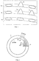
- Fig. 1 shows a graphic representation of a typical Scanning tunneling microscope image of an atomic surface, e.g. B. a crystal lattice surface on which individual atoms or Molecules (or several such particles each) 1a, 1b are arranged; the tip of a scanning tunneling microscope with the help of a piezoelectric element along predetermined Traces 2a, 2b, 2c passed over this surface and generated a tunnel current due to the very short distance very sensitive to the distance of the tip from the surface depends. By measuring this tunnel current during sampling the surface is shown in relief. By increasing the electrical voltage at the scanning tip can be individual Atoms or molecules are deposited on this surface to represent a digital bit. With certain materials, such as tungsten diselenide, the deposited Atoms are also removed and the memory is deleted become.
- a typical Scanning tunneling microscope image of an atomic surface e.g. B. a crystal lattice surface on which individual atoms or Molecules (or several such particles each)
- the storage area for one bit can e.g. 3 nm x 3 nm; the positioning accuracy must then be in the range of 0.5 nm lie.
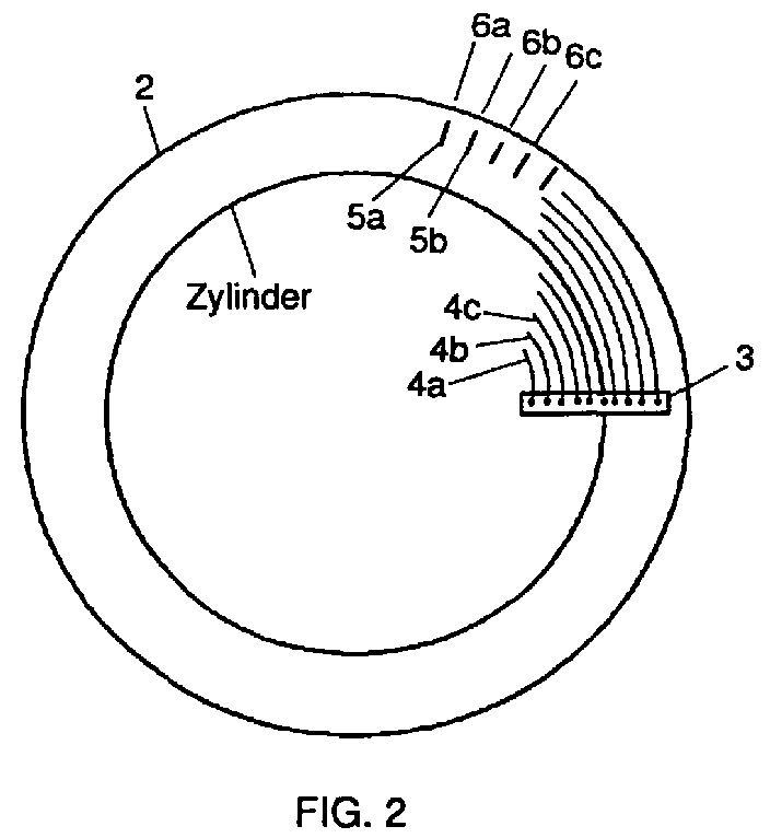
- Fig. 2 shows a storage disk 2, which is for a digital Nuclear storage like a conventional one Magnetic disk storage is provided.
- a storage layer for example made of tungsten diselenide applied in which data along circular tracks, so-called Cylinder 4a, 4b, 4c can be stored.
- the mutual spacing of the cylinders should be of the order of magnitude of 3 nm.
- These cylinders are each made up of a read / write tip described and read a scanning tunneling microscope, wherein a variety of such read / write tips in one Read / write bank 3 are connected in parallel. Typically can in the read / write bank 3 thousand or ten thousand Tips are arranged. Such read / write heads can with known lithographic methods in microtechnology getting produced.
- the storage disk 2 can have a diameter of, for example 40 mm and with 1000 scanning tunneling microscope tips with a width of 10 ⁇ m each.
- the read / write head thus has a length of approximately 1 cm and can be combined with piezoelectric actuators in one radial range of about 10 microns, so over a total of 3330 cylinder tracks 4. In this way, the total effective storage area of the storage disk 2 be scanned when the disk rotates and the read / write bench 3 is moved piezoelectrically.
- the storage area is thus in a ring on the plate between the radii 1 and 2 cm.
- This atomic storage then has a capacity of 8.7 terrabytes.
- the read or write speed is approximately 10 8 bits / sec. It takes around 200 hours to read or write to this disk completely.
- a full revolution in read or write mode takes approximately 3.5 minutes, which is orders of magnitude more than with random access memories, e.g. B. Magnetic disks with random access in the millisecond range.
- the invention proposes the periphery of the storage disk 2 positioning marks 5 to arrange, define the memory sectors 6a, 6b, 6c and whose position is interferometric with a precision of approximately 0.5 nm can be determined.
- Sector marks 5 formed as so-called ⁇ / 2 marks, which in Relation to what will be discussed later interferometric methods are discussed in more detail.
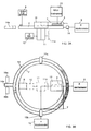
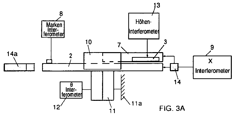
- the figures 3A and 3B schematically show one Section or supervision of an atomic storage random access and interferometric positioning according to the invention.
- the storage disk 2 is rotatable by one Center axis, not shown, stored with a suitable motor is connected for large rotary movements, e.g. B. a DC stepper motor.
- a suitable motor is connected for large rotary movements, e.g. B. a DC stepper motor.
- To the disk 2 is in closely spaced a ring 14 in which several Locking elements 15a, 15b are provided, which in brought into positive contact with the storage plate 2 can be.
- the ring 14 has a lever 14a, which with two piezoelectric displacement elements 16a, 16b connected with which the lever 14a moves in a targeted manner and thus the ring 14 can be rotated.
- Theta interferometer 12 determines that the interference of a Light beam at one with the disk 2 fixed connected prismatic glass column 11 evaluates. Details this measurement will be explained with reference to FIG. 6.
- the prismatic glass column 11 is symmetrical to the axis of rotation of the Storage disc 2 arranged. By the full rotation angle of To cover 360 ° for disk 2, two must prismatic vitreous bodies with a mutual twist of 45 degrees can be provided.
- the fine positioning of the read / write bench 3 with respect to tracks 4 of the disk are made with a Relative measurement with respect to the edge of the storage plate 2 through the X and Y interferometers that are perpendicular to each other are arranged.
- the read / write bench 3 is on one piezoelectric body 7 attached, which has a displacement can cause both in the X and Y directions.
- the X and the Y interferometer each probe with one of them Interference rays on the edge of the storage disk 2 and with their second interfering beam each have the X and Y edges of the piezoelectric block 7.
- the Read / write block controlled relative to the disk 2 shifted, which in turn from an extraordinarily stable and dimensionally stable material is built, for example Zerodur.
- the positioning remains due to this relative measurement of the read / write block 3 unaffected by mechanical Tolerances, inaccuracies, bearing play, etc., since the location of the Data tracks 4 on the disk 2 only in relation to the latter is defined
- a particularly critical parameter is the distance between the read / write tips from the surface of the disk 2. To adjust this distance optimally after using a sector fast rotating movement and raised read / write block an interferometer 13 is provided, that the distance of each read / write tip from the Disk 2 monitored.
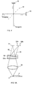
- FIG. 4 shows the principle of a Michelson interferometer, in which an input light bundle I is split into two partial light bundles by a semi-transparent mirror 41. These partial light bundles are each reflected on a mirror 42 or a measurement object 43 and the reflected bundles are combined to form an output bundle in which interference patterns occur in accordance with the phase difference between the two partial light bundles.
- the phase shift ⁇ of the partial light beams can be measured using various known methods, for example by additionally impressing three different phases with known values.
- a minimum value for the signal / noise ratio is necessary for the measurement of the phase shift with photodiodes or photomultipliers.
- the required intensities can be estimated by taking into account the various noise sources (electrical noise in photodiodes, photon noise in multipliers) and the required degree of accuracy of the positioning.
- the output intensities can be converted into an electrical current using photodiodes or multipliers and can thus be measured.
- the precision of the measurement is determined by the signal to noise ratio, S / N.
- the noise sources are for photodiodes and multipliers differently.
- the noise of the photodiodes is in the significant electrical noise.
- the essential In contrast, the source of noise in multipliers is photon noise.
- 5A shows the schematic structure of an interferometric arrangement for the precise determination of the position of the sector marks.
- the light-emitting layer of a diode laser 51 is imaged on the surface of the storage plate 2 using an imaging optics 54.
- the sector positioning mark 4 on the storage disc 2 is designed as a so-called 180 degree or ⁇ / 2 phase plate with an optical thickness of ⁇ / 4 (since it is traversed twice by the light), where ⁇ represents the wavelength of the light emitted by the laser diode 51.
- the light bundle 52 of the diode 51 passes through a Rochon prism 53 with a ⁇ / 4 plate 53a connected downstream.
- the light bundle 52 is polarized as it passes through the Rochon prism, so that the reflected light bundle 55, which has passed twice through the ⁇ / 4 plate 53a and thus has rotated its direction of polarization by 90 °, is deflected onto two photodiodes 56a, 56b arranged next to one another.
- the photodiodes 56a, 56b which can also be designed as a so-called quadrant diode, generate the difference quotient (ab) / (a + b) from the two sub-entities of light A and B in beam 55.
- Fig. 5B shows an alternative arrangement in which instead of two photodiodes 56a, 56b two photomultipliers 58a, 58b can be used on the light of the light beam 55 with With the help of a beam splitter device 57, the from a glass plate with a micromechanically manufactured Prism 57a exists.
- the advantage of using Multiplayer 58a, 58b is that the one Have photon noise.
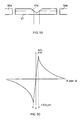
- 5C shows the output signal of the photodiodes 56a, 56b, or the photomultipliers 58a, 58b.
- the signal (ab) / (a + b) is plotted there over the displacement X or the angular displacement ⁇ .
- sector mark 4 By designing sector mark 4 as a phase plate, which when passing through the incident and then reflected Light produces a phase shift of 180 ° in total, 5C sets the output signal in FIG Represents zero crossing with a width of less than 0.5 ⁇ m. This signal form is based on the use of the 180 ° phase plate trained sector brand.
- the prerequisite for this interpolation is an adequate signal-to-noise ratio, which with the present invention is achieved.
- FIG. 6 shows the structure of a differential interferometer arrangement, those in the X and Y interferometers of FIG. 3 Can be used to determine the relative distance between the disk 2 and the read / write block 3 with one Determine precision in the subnanometer range.
- the light beam 60 of a laser passes through a lens 61 and a beam splitter 63 into a Wollaston prism 64 where it is split into two polarized sub-beams 66a, 66b, that of a lens 65 on the edge of the disk 2 or on the read / write pad 3 or the edge of the peizoelectric plate 7 are focused.
- the reflected Beams 66a, 66b then become one from beam splitter 63
- This position difference ⁇ X is when the Atomic storage kept constant with a control loop.
- the read / write block 3 In order to the read / write block 3 with a radial displacement of the Disk 2 guided on tracks that down to 0.5 nm all deviations of the edge of the disk 2 from Show ideal circle.
- this interferometric Control arrangement can therefore the memory tracks 4 (cylinder) of the atomic storage even if there are radial deviations can be reproduced reproducibly.
- a certain one of the cylinders 4 of the Atomic storage can be started, that needs 6 shows an absolute zero point.
- This zero point is determined with the help of two confocal diaphragms 62, 67, which cause the intensity in the light beam 69, which is fed to the phase evaluation unit, a maximum achieved when exactly focused.
- the zero point for the measurement is now related to this Maximum defined with exact focusing.
- This will be Measurement signal when the read / write block is in the middle 3 by rotating the disk (with the inevitable radial deviations) to an exact maximum focused. The disk 2 is then in this position and the tips together in the X direction by +/- 5 ⁇ m shifted. With this shift it will Interferometer output signal plotted over the X axis and the maximum of the envelope curve by differentiating certainly. This maximum is called the absolute zero point for the Movements in the X direction used.
- the sensitivity of this measurement method is determined by the more or less rapid drop in intensity when defocusing certainly.
- This drop in intensity can be chosen Set the numerical aperture of the lens 65.
- linear Interpolation can then be the corresponding in the measurement signal Positioning accuracy can be achieved.
- the Component in the X direction is, as described, by regulation a constant distance between the read / write block 3 and tracked the edge of the disk.
- a corresponding interferometic arrangement 10 is also for the Y direction is provided and in the same way as FIG. 6 built up.
- the absolute position of the disk edge can be determined, for example, a shift in the to be able to compensate the entire storage disk in the Y direction.
- the Interferometer 10 with two different wavelengths operated, the first wavelength ⁇ 1 in the same way as in the X direction, the difference between the read / write block 3 and the edge of the disk 2 determined.
- For the second wavelength ⁇ 2 is between lens 65 and read / write block 3 introduced a dichroic beam splitter that firmly connected to the base of the atomic storage and only Light of the second wavelength ⁇ 2 is reflected. With the help of the second wavelength ⁇ 2 determined interferometrically absolute location of the edge of the disk 2 is used to appropriate corrections in the sector count to attach.
- a diode laser can be used Location of the aperture 62 is arranged. The hole in the aperture 67 is then on the light emitting surface of the diode laser vote.
- Fig. 7 shows an interferometer arrangement for measuring the Angle of rotation within a sector.
- the square Glass prism 11 is symmetrical to the axis of rotation of the Disk 2 and is firmly connected to this.
- the Beam 71 of a laser 70 passes through semi-transparent mirror 72 and a Wollaston prism 73 and is through an imaging system 74 through the glass prism 11 a mirror 75 is shown.
- the reflected light will due to the polarization in the Wollaston prism 73 by the semi-transparent mirror 72 to a phase measuring device 76 distracted.
- the light path of two beams 71a, 71b of the laser light beam is schematic at two different angular positions of the square glass prism 11 and 11 'shown.
- the Path length difference of the two light beams can be at one square glass prism with an edge length of 10 mm to to be 30 mm.
- the one caused by it Phase difference becomes 76 in the device for phase measurement determines and allows the corresponding angle of rotation to determine. Around the full rotation range of 360 ° two square glass prisms are required to cover that are rotated by 45 ° to each other.
- a relatively small and inexpensive diode laser can be used as the laser 70 can be used because when measuring within a Storage sector does not have high demands on the relative Measurement uncertainty are made.
- This measurement uncertainty can be estimated as follows: The repeatability for the measurement of the rotary movement is determined by an angle ⁇ , which is calculated from the quotient of the lateral repeatability (0.5 nm) and the inner disk radius (10 mm).
- the angular measurement range for a storage sector is approximately 1.25 x 10 -3 rad, so that there is a relative measurement uncertainty of 4 x 10 -5 , which is technically easily manageable. If, instead, the entire storage disk was taken as a full revolution, a relative measurement uncertainty of 5 x 10 -8 rad would have to be achieved, which would not be possible or would only be possible with a very high technical outlay.
- the interferometer in Fig. 8 uses two light sources, one White light source and a (monochromatic) laser light source.
- the white light is used to measure the distance from the tips roughly adjust the memory surface to then use the laser light the fine positioning with higher accuracy and higher signal / noise ratio.
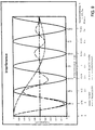
- the advantage of laser light is that a clear (directional) zero point of the interferometric measurement can be determined. This shows 8B typical interference signals for monochromatic Laser light and white light with its typical, unique Intensity maximum.
- the two light bundles 800 (I ⁇ 1 ) and 801 (I 2 ) are deflected by a semi-transparent mirror 802 and split into two partial bundles in a Wollaston prism 803 which, via imaging optics 804 and a Babinet compensator 805, cover the surface of the storage plate 2 or press the read / write head 3.
- the on the storage disk or the read / write head 3 reflected light beams pass through the semi-transparent Beam splitter 802 through and are in another Wollaston prism 806 split over an imaging lens 807 to hit a spatial light modulator 808.
- This spatial light modulator makes it possible to use electronic Ways to change the phase of the light from each one Tip is reflected in the read / write head 3.
- Such spatial light modulators are in the State of the art known.
- the spatial light modulator 808 has double according to the two light beams occurring as many modulation points as tips in the read / write head 3 are included.
- the light bundles reflected at the spatial light modulator 808 pass through imaging optics 809 into a Wollaston prism 810, where they are reunited, and reach a dichroic mirror 811, at which the monochromatic light I ⁇ 1 leads to imaging optics 813 and two arrangements 814a, 814b of photodiodes is distracted.
- the white light beam I white passes through the dichroic mirror 811 and arrives at a Wollaston prism 815, where it is split up and through imaging optics 816 to a photodiode arrangement 817, in which two photodiodes are provided for each tip in the read / write head 3 .
- the light sources for the light bundles 800 and 801 and / or the Imaging optics 804 preferably designed so that they produce a light band, that acts on all tips in the read / write head 3 in parallel.
- the image in the entire interferometic arrangement 8 is chosen so that two photodiodes in each the photodiode arrays 814 and 817 at a tip in the Read / write head 3 received and received reflected light evaluate.
- the light path in the entire interferomentric Arrangement is chosen so that the read / write tips that corresponding points of the spatial optical modulator and the pairs of photodiodes each optically to each other are conjugated.
- the pairs of photodiodes generate an output signal using a standardized difference signal.
- the standardized difference signal is independent of the illuminance and can be determined in real time. The necessary speed is thus available to prevent the tips in the read / write head 3 from being destroyed during movements in the Z direction.
- the peaks are brought up to 1 nm to the storage plate 2 with the aid of the laser interferometer of the wavelength I ⁇ 1 . From this point on, the scanning tunneling microscope itself takes over the distance control and moves the tips to the optimal working point.
- the Babinet compensator 805 serves for the rough adjustment for all tips and the spatial light modulator 808 for the individual fine adjustment of each individual tip. This means that each tip can be set so that the optimum working distance with the steepest slope of the laser interferometer is achieved with the wavelength I ⁇ 1 .
Landscapes
- Engineering & Computer Science (AREA)
- Chemical & Material Sciences (AREA)
- Nanotechnology (AREA)
- Physics & Mathematics (AREA)
- Mathematical Physics (AREA)
- Theoretical Computer Science (AREA)
- Crystallography & Structural Chemistry (AREA)
- Length Measuring Devices By Optical Means (AREA)
- Micromachines (AREA)
Abstract
Description
- Fig. 1
- eine schematische Darstellung einer Rastertunnelmikroskop-Aufnahme der Speicherfläche eines Atomspeichers mit einzelnen Bitpositionen,
- Fig. 2
- die schematische Darstellung der Formatierung der Speicherfläche eines Atomspeichers mit wahlfreiem Zugriff,
- Fig. 3A
- eine schematische Seitenansicht eines Atomspeichers mit wahlfreiem Zugriff und interferometrischen Positioniereinrichtungen,
- Fig. 3B
- eine schematische Aufsicht auf den Atomspeicher von Fig. 3A,
- Fig. 4
- die schematische Darstellung eines Michelson-Interferometers,
- Fig. 5A
- die schematische Darstellung eines Interferometers zur genauen Positionsbestimmung von Sektormarken,
- Fig. 5B
- die schematische Darstellung einer mikromechanisch hergestellten Strahlteileranordnung für zwei Photomultiplier,
- Fig. 5C
- das Ausgangssignal der Differenzschaltung zweier Dioden oder Photomultiplier im Interferometer nach Fig. 5A,
- Fig. 6
- die schematische Darstellung einer Differenz-Interferometeranordnung zur Messung der Lage von Speicherspuren in X- und Y-Richtung,
- Fig. 7
- die schematische Darstellung einer Interferometeranordnung zur Messung des Drehwinkels der Speicherscheibe,
- Fig. 8
- die schematische Darstellung eines Interferometers zur Messung der Höhe der Lese-/Schreibspitzen über der Speicherscheibe,
- Fig. 9
- Die Ausgangsignale interferometrischer Messungen mit weißem und monochromatischem Licht
Claims (15)
- Digitalspeicher mit mindestens einer Speicherfläche, auf der die digitale Information durch die Anwesenheit bzw. die Abwesenheit atomarer oder molekularer Strukturen dargestellt ist, und mit einem Schreib-/Lesekopf (3), in dem ein oder mehrere mikromechanische Spitzen zur Abtastung der Speicherfläche vorgesehen sind,
dadurch gekennzeichnet,daß die Positionierung und Führung des Schreib-/Lesekopfes auf der Speicherfläche (2) mit interferometrischen Methoden erfolgt. - Digitalspeicher nach Anspruch 1,
dadurch gekennzeichnet,daß die Speicherfläche als rotierende Scheibe (2) ausgebildet ist, auf der die digitale Information längs konzentrischer Spuren (4) aufgezeichnet wird,und daß die Spuren in Sektoren (6) unterteilt sind, deren Beginn durch Marken (5) angezeigt wird, die bei einer schnellen Drehung der Speicherfläche (2) durch eine interferometrische Vorrichtung (8) abgetastet werden. - Digitalspeicher nach Anspruch 1 oder 2,
dadurch gekennzeichnet,daß die Sektormarken als λ/4 Plättchen ausgebildet sind und von einer Interferometeranordnung erkannt werden, bei der eine Lichtquelle (51) auf die Speicherfläche (2) abgebildet wird, und das an der Speicherfläche (2) reflektierte Licht in einer optischen Differenzanordnung (56a, 56b) ausgewertet wird. - Digitalspeicher nach Anspruch 3,
dadurch gekennzeichnet,daß der lineare Teil des Ausgangssignals der optischen Differenzanordung durch elektronische Mittel interpoliert wird. - Digitalspeicher nach einem der Ansprüche 1 bis 4,
dadurch gekennzeichnet,daß zur Drehung der Speicherplatte innerhalb eines Sektors (6) eine piezoelektrische Einrichtung (14, 15, 16) vorgesehen ist, die kraftschlüssig mit der Speicherplatte (2) in Eingriff gebracht wird, nachdem die Speicherplatte auf den Beginn eines Sektors justiert ist. - Digitalspeicher nach Anspruch 5,
dadurch gekennzeichnet,daß die Positioniereinrichtung aus einem Ring (14) mit Feststellelementen (15) besteht, unddaß piezoelektrische Verstellelemente (16) auf einen mit dem Ring (14) verbundenen Hebel (14a) einwirken. - Digitalspeicher nach einem der Ansprüche 1 bis 6,
dadurch gekennzeichnet,daß zur Messung der Drehung der Speicherplatte (2) ein Interferometer (12) vorgesehen ist, das die Phasendifferenz zweier Lichtbündel mißt, die durch ein mit der Speicherplatte (2) fest verbundenes quadratisches Glasprisma (11) hindurchtreten und an einem Spiegel (11a) reflektiert werden. - Digitalspeicher nach einem der Ansprüche 1 bis 7,
dadurch gekennzeichnet,daß zur Regelung des Schreib-/Lesekopfes (3) relativ zur Lage der Spuren (4) ein Interferometer (9) vorgesehen ist, das die Relativposition des Schreib-/Lesekopfes (3) relativ zum Rand der Speicherplatte (2) bestimmt. - Digitalspeicher nach Anspruch 8,
dadurch gekennzeichnet,daß das X-Interferometer je eine punktförmige Eintrittsblende (62) und eine Ausgangsblende (67) aufweist, die optisch zueinander konjugiert sind, wodurch das Interferenzsignal bei der Null-Lage zwischen Schreib-/Lesekopf und Speicherplatte (2) einen maximalen Wert aufweist. - Digitalspeicher nach einem der Ansprüche 1 bis 9,
dadurch gekennzeichnet,daß zur Bestimmung der Abstände zwischen den Schreib-/Leseelementen (3) und der Oberfläche der Speicherplatte (2) ein Höheninterferometer (13) vorgesehen ist, in dem eine Doppelzeilenschaltung von Photodioden enthalten ist, die im optischen Strahlengang jeweils einer Spitze des Schreib-/Lesekopfes (3) zugeordnet sind, und den Abstand jeder einzelnen Spitze von der Oberfläche der Speicherplatte (2) nach einem interferometrischen Differenzverfahren bestimmen. - Digitalspeicher nach Anspruch 10,
dadurch gekennzeichnet,daß das Höheninterferometer mit zwei verschiedenen optischen Wellenlängenbereichen betrieben wird, unddaß für jeden Wellenlängenbereich eine Auswertevorrichtung (814; 817) für das Interferenzlicht vorgesehen ist. - Digitalspeicher nach einem der Ansprüche 10 und 11,
dadurch gekennzeichnet,daß einer der optischen Wellenlängenbereiche Weißlicht darstellt und zur richtungsabhängigen Grobpositionierung der Spitzen relativ zur Oberfläche der Speicherfläche (2) eingesetzt wird. - Digitalspeicher nach einem der Ansprüche 11 oder 12,
dadurch gekennzeichnet,daß einer der optischen Wellenlängenbereiche monochromatisches Laserlicht darstellt und zur Feinpositionierung des Abstands der Spitzen im Schreib-/Lesekopf (3) bezüglich der Oberfläche der Speicherplatte (2) verwendet wird. - Digitalspeicher nach einem der Ansprüche 1 bis 13,
dadurch gekennzeichnet,daß ein Y-Interferometer (10) zur Kompensation von geometrischen Verschiebungen der Speicherplatte (2) vorgesehen ist und den Abstand zwischen dem Schreib-/Lesekopf (3) und der Grundplatte des Digitalspeichers bestimmt. - Digitalspeicher nach einem der Ansprüche 1 bis 14,
dadurch gekennzeichnet,daß die Speicherplatte (2) aus einem formbeständigen keramischen Material besteht.
Applications Claiming Priority (2)
| Application Number | Priority Date | Filing Date | Title |
|---|---|---|---|
| DE1998134107 DE19834107A1 (de) | 1998-07-29 | 1998-07-29 | Atomspeicher |
| DE19834107 | 1998-07-29 |
Publications (2)
| Publication Number | Publication Date |
|---|---|
| EP0977194A2 true EP0977194A2 (de) | 2000-02-02 |
| EP0977194A3 EP0977194A3 (de) | 2005-10-26 |
Family
ID=7875685
Family Applications (1)
| Application Number | Title | Priority Date | Filing Date |
|---|---|---|---|
| EP99110080A Withdrawn EP0977194A3 (de) | 1998-07-29 | 1999-05-22 | Atomspeicher |
Country Status (2)
| Country | Link |
|---|---|
| EP (1) | EP0977194A3 (de) |
| DE (1) | DE19834107A1 (de) |
Cited By (1)
| Publication number | Priority date | Publication date | Assignee | Title |
|---|---|---|---|---|
| DE102012023526A1 (de) * | 2012-11-30 | 2014-06-05 | Christoph Hiller | Steigerung der Kapazität von Datenleitungen und Computerspeichern |
Family Cites Families (13)
| Publication number | Priority date | Publication date | Assignee | Title |
|---|---|---|---|---|
| DE6903004U (de) * | 1969-01-27 | 1970-07-09 | Mebeda Fa | Instrument fuer die intra- uterusbehandlung. |
| US3791736A (en) * | 1972-04-28 | 1974-02-12 | Us Air Force | Method and apparatus utilizing the phase velocity difference of light rays for measuring the velocity of a moving object |
| US4124872A (en) * | 1977-01-26 | 1978-11-07 | Propst Franklin M | Record/playback apparatus |
| US4340305A (en) * | 1977-05-03 | 1982-07-20 | Massachusetts Institute Of Technology | Plate aligning |
| US4464689A (en) * | 1981-06-04 | 1984-08-07 | Education & Informations Systems, Inc. | Random access read/write unit |
| US4613916A (en) * | 1983-12-30 | 1986-09-23 | International Business Machines Corporation | Information storage disk transducer position control system requiring no servo pattern on the storage disk |
| DE3706277C2 (de) * | 1986-02-28 | 1995-04-27 | Canon Kk | Drehungsmeßgeber |
| JP2683117B2 (ja) * | 1989-10-31 | 1997-11-26 | キヤノン株式会社 | エンコーダー |
| JP2999282B2 (ja) * | 1990-03-09 | 2000-01-17 | キヤノン株式会社 | 記録再生方法及び装置 |
| US5107107A (en) * | 1990-03-30 | 1992-04-21 | The United States Of America As Represented By The Administarator Of The National Aeronautics And Space Administration | Laser optical disk position encoder with active heads |
| JP3387690B2 (ja) * | 1995-04-18 | 2003-03-17 | キヤノン株式会社 | 基準信号発生装置及びそれを用いた回転情報検出装置 |
| JPH07294229A (ja) * | 1994-04-28 | 1995-11-10 | Canon Inc | 角度分割装置 |
| US5602820A (en) * | 1995-08-24 | 1997-02-11 | International Business Machines Corporation | Method and apparatus for mass data storage |
-
1998
- 1998-07-29 DE DE1998134107 patent/DE19834107A1/de not_active Ceased
-
1999
- 1999-05-22 EP EP99110080A patent/EP0977194A3/de not_active Withdrawn
Cited By (1)
| Publication number | Priority date | Publication date | Assignee | Title |
|---|---|---|---|---|
| DE102012023526A1 (de) * | 2012-11-30 | 2014-06-05 | Christoph Hiller | Steigerung der Kapazität von Datenleitungen und Computerspeichern |
Also Published As
| Publication number | Publication date |
|---|---|
| EP0977194A3 (de) | 2005-10-26 |
| DE19834107A1 (de) | 2000-02-03 |
Similar Documents
| Publication | Publication Date | Title |
|---|---|---|
| DE69032386T2 (de) | Optisches Aufzeichnungs/Wiedergabesystem und -verfahren, optisches Medium | |
| DE2909770C2 (de) | Aufzeichnungsträgerkörper, der aus einem runden scheibenförmigen Substrat besteht, und Vorrichtung zum Einschreiben in einen und Auslesen aus einem solchen Aufzeichnungsträger | |
| DE69330357T2 (de) | Optische Speichervorrichtung | |
| DE3889509T2 (de) | Optische Abtastvorrichtung und optische Gitteranordnung dazu. | |
| DE69019913T2 (de) | Atomkraftmikroskop. | |
| DE4135011C2 (de) | Bildplattengerät | |
| DE69133432T2 (de) | Mehrschichtinformationsspeichersystem | |
| DE69227397T2 (de) | Informationsverarbeitungsvorrichtung | |
| DE69317731T2 (de) | Optischer Abtastkopf | |
| DE19513273B4 (de) | Opto-magnetische Kopfanordnung | |
| DE4029040C2 (de) | ||
| DE2522405A1 (de) | Optisches mehrkanal-plattenspeichersystem zum speichern von digitaler information | |
| CH660810A5 (de) | Anordnung zum schreiben und lesen von datenspuren in einem optischen aufzeichnungstraeger. | |
| EP0011708A1 (de) | Verfahren und Vorrichtung zur Messung der Ebenheit, der Rauhigkeit oder des Krümmungsradius einer Messfläche | |
| DE69011188T2 (de) | Kodierer. | |
| DE69727186T2 (de) | Vorrichtung zur Aufzeichnung und Wiedergabe eines optischen Aufzeichnungsträgers | |
| DE68924524T2 (de) | Optische Abtastvorrichtung und geeignetes Spiegelobjektiv zum Anpassen an diese Vorrichtung. | |
| DE102008007319A1 (de) | Optische Positionsmesseinrichtung | |
| DE3445751A1 (de) | Einrichtung zum halten mehrerer lichtstrahlen in vorbestimmten relativen lagen | |
| DE69832244T2 (de) | Vorrichtung zur Wiedergabe und Aufzeichnung eines optischen Speichermedium | |
| DE19930687B4 (de) | Optisches Verschiebungsmeßsystem | |
| DE3137211C2 (de) | Vorrichtung zur Bestimmung der Bewegung eines Gegenstandes mit einem Interferometer | |
| DE69702799T2 (de) | Vorrichtung und Verfahren zur Spurverfolgung | |
| EP1295286B1 (de) | Gerät zum lesen und/oder beschreiben optischer aufzeichnungsträger | |
| DE2914122C2 (de) | Opto-elektronische Einrichtung zur Erzeugung eines Fokussierungssignals |
Legal Events
| Date | Code | Title | Description |
|---|---|---|---|
| PUAI | Public reference made under article 153(3) epc to a published international application that has entered the european phase |
Free format text: ORIGINAL CODE: 0009012 |
|
| AK | Designated contracting states |
Kind code of ref document: A2 Designated state(s): AT BE CH CY DE DK ES FI FR GB GR IE IT LI LU MC NL PT SE |
|
| AX | Request for extension of the european patent |
Free format text: AL;LT;LV;MK;RO;SI |
|
| PUAL | Search report despatched |
Free format text: ORIGINAL CODE: 0009013 |
|
| AK | Designated contracting states |
Kind code of ref document: A3 Designated state(s): AT BE CH CY DE DK ES FI FR GB GR IE IT LI LU MC NL PT SE |
|
| AX | Request for extension of the european patent |
Extension state: AL LT LV MK RO SI |
|
| AKX | Designation fees paid | ||
| STAA | Information on the status of an ep patent application or granted ep patent |
Free format text: STATUS: THE APPLICATION IS DEEMED TO BE WITHDRAWN |
|
| 18D | Application deemed to be withdrawn |
Effective date: 20051103 |
|
| REG | Reference to a national code |
Ref country code: DE Ref legal event code: 8566 |