EP0978005B1 - Composant optique miniaturise, et mode de fabrication - Google Patents
Composant optique miniaturise, et mode de fabrication Download PDFInfo
- Publication number
- EP0978005B1 EP0978005B1 EP98921483A EP98921483A EP0978005B1 EP 0978005 B1 EP0978005 B1 EP 0978005B1 EP 98921483 A EP98921483 A EP 98921483A EP 98921483 A EP98921483 A EP 98921483A EP 0978005 B1 EP0978005 B1 EP 0978005B1
- Authority
- EP
- European Patent Office
- Prior art keywords
- parts
- devices
- moulding
- adjustment means
- process according
- Prior art date
- Legal status (The legal status is an assumption and is not a legal conclusion. Google has not performed a legal analysis and makes no representation as to the accuracy of the status listed.)
- Expired - Lifetime
Links
Images


Classifications
-
- G—PHYSICS
- G01—MEASURING; TESTING
- G01J—MEASUREMENT OF INTENSITY, VELOCITY, SPECTRAL CONTENT, POLARISATION, PHASE OR PULSE CHARACTERISTICS OF INFRARED, VISIBLE OR ULTRAVIOLET LIGHT; COLORIMETRY; RADIATION PYROMETRY
- G01J3/00—Spectrometry; Spectrophotometry; Monochromators; Measuring colours
- G01J3/02—Details
- G01J3/0202—Mechanical elements; Supports for optical elements
-
- G—PHYSICS
- G01—MEASURING; TESTING
- G01J—MEASUREMENT OF INTENSITY, VELOCITY, SPECTRAL CONTENT, POLARISATION, PHASE OR PULSE CHARACTERISTICS OF INFRARED, VISIBLE OR ULTRAVIOLET LIGHT; COLORIMETRY; RADIATION PYROMETRY
- G01J3/00—Spectrometry; Spectrophotometry; Monochromators; Measuring colours
- G01J3/02—Details
- G01J3/0205—Optical elements not provided otherwise, e.g. optical manifolds, diffusers, windows
- G01J3/0243—Optical elements not provided otherwise, e.g. optical manifolds, diffusers, windows having a through-hole enabling the optical element to fulfil an additional optical function, e.g. a mirror or grating having a throughhole for a light collecting or light injecting optical fiber
-
- G—PHYSICS
- G01—MEASURING; TESTING
- G01J—MEASUREMENT OF INTENSITY, VELOCITY, SPECTRAL CONTENT, POLARISATION, PHASE OR PULSE CHARACTERISTICS OF INFRARED, VISIBLE OR ULTRAVIOLET LIGHT; COLORIMETRY; RADIATION PYROMETRY
- G01J3/00—Spectrometry; Spectrophotometry; Monochromators; Measuring colours
- G01J3/02—Details
- G01J3/0256—Compact construction
-
- G—PHYSICS
- G01—MEASURING; TESTING
- G01J—MEASUREMENT OF INTENSITY, VELOCITY, SPECTRAL CONTENT, POLARISATION, PHASE OR PULSE CHARACTERISTICS OF INFRARED, VISIBLE OR ULTRAVIOLET LIGHT; COLORIMETRY; RADIATION PYROMETRY
- G01J3/00—Spectrometry; Spectrophotometry; Monochromators; Measuring colours
- G01J3/02—Details
- G01J3/0291—Housings; Spectrometer accessories; Spatial arrangement of elements, e.g. folded path arrangements
-
- B—PERFORMING OPERATIONS; TRANSPORTING
- B29—WORKING OF PLASTICS; WORKING OF SUBSTANCES IN A PLASTIC STATE IN GENERAL
- B29L—INDEXING SCHEME ASSOCIATED WITH SUBCLASS B29C, RELATING TO PARTICULAR ARTICLES
- B29L2011/00—Optical elements, e.g. lenses, prisms
Definitions
- the invention relates to a miniaturized optical component comprising at least two components, of which at least one component is optical microstructures has, the components spaced from each other via at least one Spacer bodies are interconnected, and the components and the Spacer body self-adjusting adjustment means for a precise Relative adjustment when assembling the components and the Have molded spacer.
- the invention also relates to a Process for the production of such miniaturized optical components.
- DE 3611246 C2 proposed that optical components of the component including the or Echelette grating on X-ray lithography, X-ray depth lithography galvanoplastic or derived from this impression technique to produce, the grid lines parallel to the X-rays.
- this method has the disadvantage that three-dimensional structures, such as. mirrors curved in two planes cannot be produced, because in the direction of x-rays because of the linear propagation no structuring is possible.
- LIGA technology opens up a great deal in terms of microtechnical processes Variety of shapes and materials as well as high precision of the detail structures (see e.g. W. Ehrfeld. H. Lehr, Rad. Physics and Chemistry, 1995. Pergamon Press). This creates mold inserts that are different Impression techniques can be replicated as plastic, metal or ceramic parts can and structuring only on the side walls of the hollow body exhibit.
- the side wall profile (e.g. grille, mirror) is transferred to the hollow body.
- the optical elements have a curvature only in one plane, so that the light is focused only in this plane.
- a Layer waveguide arrangement used, the height of which is limited (see e.g. Interdisciplinary Science Reviews, 1993, 18, No. 3, p. 273).
- An optical component is known from US 5,521,763, however does not represent a miniaturized component with an optical microstructure.
- a common base plate is a toroidal lens, a polygonal Mirror and a detector arranged. However, it is not about self-adjusting means of adjustment because the plug-in elements are inserted in elongated holes become. It is fixed with adhesive and springs.
- Japanese abstract 61-144609 denotes an optical coupling element, which comprises two optical components mounted on a vertical base plate are attached. About the type of attachment and adjustment are not Information provided.
- EP 0 194 613 describes a method for adjusting optical assembly Components known.
- the optical components are with exact location and Alignment created and assembled and fixed in a defined manner.
- the components have step-like structures as adjustment elements. about Spacer moldings that have appropriate adjustment structures, the optical components arranged at a distance from each other. The items need be assembled for assembly, taking care. which components have to be put together and how.
- the miniaturized optical component is characterized in that at least two parts are connected to one another via connecting means and form a coherent unit.
- the connecting means ensure an association of the two connected individual parts, so that the related together during assembly Components are immediately recognizable.
- the connecting means are preferably so designed and attached to the components that the assembly clearly is set.
- Another advantage is that the connecting means Represent loss protection.
- the individual components are offered in a set, especially for mass production and only assembled by the user. So that the individual related parts are not lost, it is beneficial if all Components are connected to one another via suitable connecting means and form a coherent unit.
- suitable connecting means are lanyards preferably elastic and can, for example, elastic fiber ribbon or be film hinges.
- These connecting means are advantageously made of made of the same material as the components, which means that the Manufacturing process is simplified.
- the elastic connecting means are preferably on the non-structured Wall surface of the parts arranged, which has the advantage that the individual parts can be assembled without cutting through the connecting means Need to become.
- the individual parts can also be disassembled and remain connected to each other via the connecting means.
- Adjustment means the desired mutual alignment and positioning of the Automatically adjusts parts.
- the type of adjustment device used does not only depend on the number of parts and their mutual arrangement, but also on the desired precision.
- the adjustment means preferably act form-fitting together.
- optical component variable The fact that several individual parts are assembled with high precision can, is the geometric embodiment of the optical component variable. This is particularly important if e.g. miniature spectrometer should be produced because in this way a free jet optics can be realized.
- a free space remains between the components so that the light propagates only takes place in a material-free room. This has the advantage that no resolution-reducing dispersion, e.g. in glass or plastic occurs.
- optical microstructures are preferably only on one side of the parts arranged, which simplifies the production with appropriate shapes.
- the shaped spacer body is preferably a base plate, in particular a base plate for the other parts common plug-in board, the adjustment means with the corresponding adjustment means on the other parts.
- the Adjustment means can be recesses and / or projections into which the remaining parts are inserted with appropriate adjustment means. Particularly in the mass production of miniaturized moldings through differently designed plug-in boards the mutual assignment of the remaining parts can be varied in a simple manner without the rest Individual components with structures on their surfaces, need to be changed. This creates a high degree of flexibility Maintaining the precision with respect to the mutual arrangement achieved.
- the adjustment means are preferably molded onto or into the parts formed.
- the manufacture and attachment of the adjustment means is thus in shifted the manufacturing process of the parts so that the adjustment of the parts is determined by the mold for the manufacture of the parts. So there are only high-precision molds required with which a mass production high-precision components with integrated adjustment means is possible.
- the optical component is a miniaturized spectrometer, this indicates first component preferably at least one planar or curved Diffraction grating structure and / or at least one connection structure for polychromatic and / or monochromatic light.
- this in the assembled state as Lattice girder part formed component opposite part at least one planar or curved concave mirror structure.
- the first component can be a curved one Diffraction grating structure and a second component at least one Have connection structure for light.
- At least one component preferably has at least one recess Recording a detector.
- the microspectrometer is sealed light-tight to the environment at least one cover part is provided, which has adjustment means which with corresponding adjustment means on at least one of the other components interact.
- the cover can also be U-shaped and therefore three Have walls.
- the process for producing such miniaturized components is thereby characterized in that the components and the at least one molded spacer together with their self-adjusting adjustment means in one step are produced by molding, with at least two parts together and via connecting means as a coherent unit are manufactured.
- the connecting means are preferably made of the same material as that Components and can therefore advantageously in the same manufacturing step getting produced.
- Insert connecting means also from others Materials than the components can consist of.
- a microtechnically produced mold insert is advantageous used because the impression-making production is inexpensive Production in large numbers allowed.
- microstructures only apply to each one side of the parts is only one for impression-making essentially planar mold insert with microstructures on the top necessary.
- Such a mold insert is particularly good with microtechnical processes can be realized.
- Insert parts can be used in the molding of the spectrometer be provided. These inserts are placed in the mold cavity and partially or completely when filling the molding compound enclosed. It can be advantageous to have the largest possible area the form already to be filled in by the inserts, so that there is little space remains for the molding compound.
- the parts are to be further processed after the molding process, as is the case with optical components, e.g. still be mirrored , it is advisable to manufacture the parts so that they all have structures provided wall surfaces of the parts lie in a common plane. It is This enables the unit consisting of several parts into one Introduce coating system and the coating process only from from one side.
- Suitable processes are plasma processes, vapor deposition processes. Sputtering or electroplating processes possible. Preferably, an area and / or structure-selective mirroring performed.
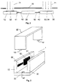
- connection means in the form of film hinges 60, 61, 62 and 63 are interconnected.
- the parts 10 and 30 have optical Structures 50, 51, 52, 53 and 54 that together make up a miniature spectrometer form.
- the part 10 is a lattice girder part and has 11 on its wall surface a structure 50 in which the image plane lies and which, for example, is one Can be a recess for a detector, a flat grid 52 and a Connection structure 51.
- the wall surface 13 is 40 in with two adjustment means Form of cuboid projections 41 provided. Between these two Projections 41, the two film hinges 60 and 61 are arranged.
- the lower wall surface 14 and the remaining wall surfaces, of which the Wall surface 12 can be seen are not structured.
- the further component 30 has two on its wall surface 31 Concave mirror structures 53 and 54 which are arranged side by side.
- the Wall surface 34 also carries adjustment means 40 in the form of cuboid Protrusions 42, between which the Fimschamiere 62 and 63 are located.
- the wall surfaces 23 and 24 on the film hinges 60 to 64 is connected to components 10 and 30.
- a total of four recesses 43 are arranged as adjustment means 40, the Dimensions are matched to the projections 41 and 42 so that the Parts 10 and 30 are inserted in a form-fitting manner in the plug-in plate 20 can.
- the film hinge must first 60, 61, 62, 63 are completely removed, as described below becomes.
- the arrangement of the adjustment means 40 is the spatial assignment of the optical Components 50 to 54 clearly defined.
- FIGS. 4a, 4b and 5a and 5b Further embodiments of the adjustment means are shown in FIGS. 4a, 4b and 5a and 5b, the connecting means for the sake of clarity were omitted.
- 4a are paired snap elements 44a and 44b formed on part 30.
- Each snap element consists of a long one Leg 45, which is arranged at right angles on the component 30, and one short leg 46 arranged at right angles thereto, which at the free end of the long leg 45 is formed.
- the plug-in plate 20 has as a corresponding Adjustment means 40 recesses in the form of openings 43 into which the Snap elements 44a and 44b can be inserted. Since the Snap element pairs 44a and 44b are each designed to be elastic these are moved towards each other for insertion, so that the two short Leg 46 fit into the opening 43 of the plug-in plate 20.
- FIG. 5a A further embodiment is shown in FIG. 5a.
- the plug-in plate 20 has as adjustment means 40 a T-shaped rail 47, the corresponding one Counterpart in component 30 in the form of an H-shaped recess 48 is provided.
- the plug-in plate 20 can by means of this T-shaped section or T-shaped rail 47 inserted into the H-shaped recess 48 become. indicated this is shown in Fig. 5b.
- Both components 20 and 30 are fixed to each other in this way.
- component 30 preferably has a lateral projection on (not visible in Fig. 5a, b), which is used for stop adjustment.
- the component 30 has a receptacle for a glass fiber and that Component 10 is a concave curved grating 52. Outside of that in FIGS. 6 and 7 Another sectional plane is shown in component 30 Recording for a detector.
- step Structures 40, 43 reached.
- the edge of these structures is determined by the mask and is therefore high Precision aligned to the other structures.
- a durable connection of the components can be during or after the Assembly, e.g. by applying an adhesive, by laser welding or Establish similar connection techniques at the joints of the individual parts.
Landscapes
- Physics & Mathematics (AREA)
- Spectroscopy & Molecular Physics (AREA)
- General Physics & Mathematics (AREA)
- Mechanical Light Control Or Optical Switches (AREA)
- Mounting And Adjusting Of Optical Elements (AREA)
Abstract
Claims (22)
- Composant optique miniaturisé qui est formé, avant l'assemblage des pièces constitutives, d'au moins deux pièces dont l'une au moins présente des microstructures optiques, les pièces (10, 30), espacées l'une de l'autre, étant reliées entre elles par l'intermédiaire d'au moins un corps moulé d'espacement (20), et les pièces (10, 30) et le corps moulé d'espacement (20) comportant des moyens d'ajustage (40) à ajustage automatique pour un ajustage relatif précis lors de l'assemblage des pièces (10, 30) et du corps moulé d'espacement, caractérisé en ce qu'au moins deux pièces (10, 20, 30) sont reliées entre elles par des moyens de lien (60-63) constituant une sécurité contre la perte et forment une unité solidaire.
- Composant selon la revendication 1, caractérisé en ce que le corps moulé d'espacement est une plaque à enfichage qui est commune aux pièces (10, 30) et dont les moyens d'ajustage (40) coopèrent avec des moyens d'ajustage (40) correspondants sur les autres pièces (10, 30).
- Composant selon l'une des revendications 1 ou 2, caractérisé en ce que les moyens d'ajustage (40) sont des éléments d'enfichage (41, 42), des éléments à enclenchement (44a, 44b), des éléments coulissants (47, 48), des saillies (41, 42) et/ou des évidements (43).
- Composant selon l'une des revendications 1 à 3, caractérisé en ce que les moyens d'ajustage (40) sont moulés sur et/ou dans les pièces (10, 20, 30).
- Composant selon la revendication 4, caractérisé en ce que les moyens de lien sont des bandes en fibres élastiques ou des charnières films (60-63).
- Composant selon la revendication 4 ou 5, caractérisé en ce que les moyens de lien sont constitués du même matériau que les pièces (10, 20, 30).
- Composant selon l'une des revendications 4 à 6, caractérisé en ce que les moyens de lien sont élastiques et sont ménagés sur la surface de paroi (14, 34) des pièces (10, 30) tournée à l'opposé de la surface de paroi structurée (11, 31).
- Composant selon l'une des revendications 1 à 7, caractérisé en ce qu'une première pièce (10) comporte au moins une structure de réseau de diffraction (52) planaire ou courbe et/ou au moins une structure de raccordement (51) pour une lumière polychromatique et/ou monochromatique et qu'une deuxième pièce (30), située en vis-à-vis de la première pièce (10) à l'état assemblé, comporte au moins une structure de miroir concave (53, 54) plan ou courbe.
- Composant selon l'une des revendications 1 à 8, caractérisé en ce qu'une première pièce (10) comporte une structure de réseau de diffraction courbe et une deuxième pièce (30) au moins une structure de raccordement pour de la lumière.
- Composant selon l'une des revendications 1 à 9, caractérisé en ce qu'au moins une pièce (10, 30) comporte au moins un évidemment destiné à recevoir un détecteur.
- Composant selon l'une des revendications 1 à 10, caractérisé en ce qu'il est prévu au moins une pièce de recouvrement (80) qui comporte des moyens d'ajustage (40) qui coopèrent avec des moyens d'ajustage (40) correspondants sur au moins une des autres pièces (10, 20, 30).
- Procédé de fabrication d'un composant optique miniaturisé formé d'au moins deux pièces (10, 30), dont l'une au moins présente des microstructures optiques (51-54), et d'au moins un corps moulé d'espacement (20), les pièces (10-30) étant assemblées par l'intermédiaire de moyens d'ajustage (40), caractérisé en ce que les pièces (10, 30) et le corps moulé d'espacement (20), au nombre d'au moins un, sont respectivement fabriqués, conjointement avec leurs moyens d'ajustage (40) à ajustage automatique, par moulage en une opération, au moins deux pièces (10, 20, 30) étant fabriquées ensemble et formant une unité solidaire par l'intermédiaire de moyens de lien (60-63).
- Procédé selon la revendication 12, caractérisé en ce que les moyens de lien (60-63) sont fabriqués dans le même matériau que les pièces (10, 20, 30) et au cours de la même étape de fabrication.
- Procédé selon la revendication 12, caractérisé en ce que des moyens de lien (60-63) sont mis en place pour le moulage lors de ou avant la fabrication des pièces (10, 20, 30).
- Procédé selon l'une des revendications 12 à 14, caractérisé en ce que des pièces mises en place pour le moulage sont noyées lors de la fabrication par moulage.
- Procédé selon la revendication 15, caractérisé en ce que l'on utilise des pièces mises en place pour le moulage en un matériau métallique ou céramique.
- Procédé selon l'une des revendications 12 à 16, caractérisé en ce que l'on a recours à un procédé de moulage par injection, de moulage réactif ou à un procédé de moulage par transfert.
- Procédé selon l'une des revendications 12 à 17, caractérisé en ce que les pièces (10, 20, 30) sont fabriquées de telle façon que toutes leurs surfaces de paroi pourvues de structures soient situées dans un plan commun.
- Procédé selon l'une des revendications 12 à 18, caractérisé en ce que les pièces (10, 20, 30), agencées à plat, sont insérées ensemble dans un dispositif d'enduction.
- Procédé selon l'une des revendications 12 à 19, caractérisé en ce que des microstructures (51-54) situées dans un plan commun font l'objet d'un traitement sélectif vis-à-vis des surfaces et/ou des structures.
- Procédé selon l'une des revendications 12 à 20, caractérisé en ce qu'un traitement sélectif vis-à-vis des surfaces et/ou des structures s'effectue au moyen d'un procédé à plasma, par dépôt par évaporation sous vide, par pulvérisation ou par galvanisation.
- Procédé selon l'une des revendications 12 ou 21, caractérisé en ce que l'on procède à un dépôt réfléchissant qui est sélectif vis-à-vis des surfaces et/ou des structures.
Applications Claiming Priority (3)
| Application Number | Priority Date | Filing Date | Title |
|---|---|---|---|
| DE19717015 | 1997-04-23 | ||
| DE19717015A DE19717015A1 (de) | 1997-04-23 | 1997-04-23 | Miniaturisiertes optisches Bauelement sowie Verfahren zu seiner Herstellung |
| PCT/EP1998/002402 WO1998048307A1 (fr) | 1997-04-23 | 1998-04-23 | Composant optique miniaturise, et mode de fabrication |
Publications (2)
| Publication Number | Publication Date |
|---|---|
| EP0978005A1 EP0978005A1 (fr) | 2000-02-09 |
| EP0978005B1 true EP0978005B1 (fr) | 2002-03-27 |
Family
ID=7827419
Family Applications (1)
| Application Number | Title | Priority Date | Filing Date |
|---|---|---|---|
| EP98921483A Expired - Lifetime EP0978005B1 (fr) | 1997-04-23 | 1998-04-23 | Composant optique miniaturise, et mode de fabrication |
Country Status (3)
| Country | Link |
|---|---|
| EP (1) | EP0978005B1 (fr) |
| DE (2) | DE19717015A1 (fr) |
| WO (1) | WO1998048307A1 (fr) |
Cited By (1)
| Publication number | Priority date | Publication date | Assignee | Title |
|---|---|---|---|---|
| US7081955B2 (en) | 2003-05-28 | 2006-07-25 | Hamamatsu Photonics K.K. | Photodetector and spectrometer using the same |
Families Citing this family (18)
| Publication number | Priority date | Publication date | Assignee | Title |
|---|---|---|---|---|
| WO2000040935A1 (fr) | 1999-01-08 | 2000-07-13 | Adc Telecommunications, Inc. | Spectrometre |
| JP4627402B2 (ja) * | 2003-11-28 | 2011-02-09 | 浜松ホトニクス株式会社 | 光検出器を用いた分光器 |
| US8068223B2 (en) | 2007-06-08 | 2011-11-29 | Hamamatsu Photonics K.K. | Spectroscopic module |
| WO2008149940A1 (fr) | 2007-06-08 | 2008-12-11 | Hamamatsu Photonics K.K. | Module spectroscopique |
| JP4891840B2 (ja) * | 2007-06-08 | 2012-03-07 | 浜松ホトニクス株式会社 | 分光モジュール |
| EP2063238B1 (fr) | 2007-06-08 | 2018-08-22 | Hamamatsu Photonics K.K. | Spectroscope |
| JP4887221B2 (ja) | 2007-06-08 | 2012-02-29 | 浜松ホトニクス株式会社 | 分光モジュール |
| JP4891841B2 (ja) | 2007-06-08 | 2012-03-07 | 浜松ホトニクス株式会社 | 分光モジュール |
| US8049887B2 (en) | 2007-06-08 | 2011-11-01 | Hamamatsu Photonics K.K. | Spectroscopic module |
| JP5512961B2 (ja) | 2008-05-15 | 2014-06-04 | 浜松ホトニクス株式会社 | 分光モジュール及びその製造方法 |
| JP5205241B2 (ja) * | 2008-05-15 | 2013-06-05 | 浜松ホトニクス株式会社 | 分光モジュール |
| JP5415060B2 (ja) | 2008-05-15 | 2014-02-12 | 浜松ホトニクス株式会社 | 分光モジュール |
| JP5207938B2 (ja) | 2008-05-15 | 2013-06-12 | 浜松ホトニクス株式会社 | 分光モジュール及び分光モジュールの製造方法 |
| JP5205240B2 (ja) | 2008-05-15 | 2013-06-05 | 浜松ホトニクス株式会社 | 分光モジュールの製造方法及び分光モジュール |
| JP5205243B2 (ja) | 2008-05-15 | 2013-06-05 | 浜松ホトニクス株式会社 | 分光器 |
| JP5205238B2 (ja) | 2008-05-15 | 2013-06-05 | 浜松ホトニクス株式会社 | 分光モジュール |
| JP2009300418A (ja) | 2008-05-15 | 2009-12-24 | Hamamatsu Photonics Kk | 分光モジュール |
| JP5718091B2 (ja) * | 2011-02-23 | 2015-05-13 | 浜松ホトニクス株式会社 | 分光モジュール |
Family Cites Families (14)
| Publication number | Priority date | Publication date | Assignee | Title |
|---|---|---|---|---|
| DE3216516A1 (de) * | 1982-05-03 | 1983-11-03 | Siemens AG, 1000 Berlin und 8000 München | Optischer wellenlaengendemultiplexer nach dem beugungsgitterprinzip |
| DE3422972C2 (de) * | 1984-06-22 | 1986-12-11 | Quante Fernmeldetechnik GmbH, 5600 Wuppertal | Vorrichtung zum Positionieren und Fixieren von Lichtleitfasern in einer parallelen Anordnung zu einem Lichtleitfaserarray |
| JPS61144609A (ja) * | 1984-12-18 | 1986-07-02 | Omron Tateisi Electronics Co | 2つの基板間の光結合装置 |
| DE3509131A1 (de) * | 1985-03-14 | 1986-09-18 | Fa. Carl Zeiss, 7920 Heidenheim | Verfahren zur justierten montage der optischen bauteile eines optischen geraetes |
| DE3611246A1 (de) * | 1986-04-04 | 1987-10-15 | Kernforschungsz Karlsruhe | Verfahren zum herstellen eines passiven optischen bauelements mit einem oder mehreren echelette-gittern und nach diesem verfahren hergestelltes bauelement |
| US5026160A (en) * | 1989-10-04 | 1991-06-25 | The United States Of America As Represented By The Secretary Of The Navy | Monolithic optical programmable spectrograph (MOPS) |
| DE4038638A1 (de) * | 1990-12-04 | 1992-06-11 | Zeiss Carl Fa | Diodenzeilen-spektrometer |
| CA2098832A1 (fr) * | 1990-12-21 | 1992-06-22 | Mark W. Beranek | Spectrographe a guide de lumiere planar |
| JPH0534617A (ja) * | 1991-07-26 | 1993-02-12 | Minolta Camera Co Ltd | レーザビーム走査光学装置 |
| DE4212208A1 (de) * | 1992-04-10 | 1993-10-14 | Bosch Gmbh Robert | Verfahren zur Herstellung optischer Polymerbauelemente mit integrierter Faser-Chip-Kopplung in Abformtechnik |
| US5216727A (en) * | 1992-05-08 | 1993-06-01 | At&T Bell Laboratories | Integrated nonlinear waveguide spectrometer |
| DE4423842C2 (de) * | 1993-07-07 | 1997-04-30 | Hirschmann Richard Gmbh Co | Steckverbinder für Lichtwellenleiter und Formeinsatz zur Herstellung desselben |
| DE4340103A1 (de) * | 1993-11-22 | 1995-05-24 | Lange Gmbh Dr Bruno | Spektralphotometer mit Beugungsgitter |
| AU5436696A (en) * | 1995-07-05 | 1997-02-05 | Lockheed Martin Energy Systems, Inc. | Monolithic spectrometer and method for fabricating same |
-
1997
- 1997-04-23 DE DE19717015A patent/DE19717015A1/de not_active Withdrawn
-
1998
- 1998-04-23 EP EP98921483A patent/EP0978005B1/fr not_active Expired - Lifetime
- 1998-04-23 DE DE59803518T patent/DE59803518D1/de not_active Expired - Fee Related
- 1998-04-23 WO PCT/EP1998/002402 patent/WO1998048307A1/fr not_active Ceased
Cited By (1)
| Publication number | Priority date | Publication date | Assignee | Title |
|---|---|---|---|---|
| US7081955B2 (en) | 2003-05-28 | 2006-07-25 | Hamamatsu Photonics K.K. | Photodetector and spectrometer using the same |
Also Published As
| Publication number | Publication date |
|---|---|
| EP0978005A1 (fr) | 2000-02-09 |
| WO1998048307A1 (fr) | 1998-10-29 |
| DE19717015A1 (de) | 1998-10-29 |
| DE59803518D1 (de) | 2002-05-02 |
Similar Documents
| Publication | Publication Date | Title |
|---|---|---|
| EP0978005B1 (fr) | Composant optique miniaturise, et mode de fabrication | |
| EP0242574B1 (fr) | Procédé pour la fabrication d'un composant optique passif à un ou plusieurs réseaux-échelette et dispositif fabriqué selon ledit procédé | |
| DE3509131A1 (de) | Verfahren zur justierten montage der optischen bauteile eines optischen geraetes | |
| DE19619353A1 (de) | Verfahren zur Herstellung eines integriert optischen Wellenleiterbauteiles sowie Anordnung | |
| EP0429877B1 (fr) | Dispositif de positionnement de fibres optiques dans des éléments de connexion | |
| EP0978006B1 (fr) | Procede de fabrication d'une piece moulee, et moule a utiliser avec ce procede | |
| DE10359576A1 (de) | Verfahren zur Herstellung einer optischen Einheit | |
| DE102007038786B4 (de) | Vorsatzlinse eines Leuchtmoduls, Leuchtmodul und Herstellungsverfahren | |
| EP0922981A2 (fr) | Corps joints | |
| DE3615821A1 (de) | Sockel fuer ein gebissmodell und verfahren zur herstellung eines gebissmodells | |
| DE3801764A1 (de) | Wellenlaengenmultiplexer oder -demultiplexer, sowie verfahren zur herstellung des wellenlaengenmultiplexers oder -demultiplexers | |
| EP1451617B1 (fr) | Miroir, systeme de representation optique et leur utilisation | |
| DE4200397C1 (fr) | ||
| DE4423842C2 (de) | Steckverbinder für Lichtwellenleiter und Formeinsatz zur Herstellung desselben | |
| EP1395859B1 (fr) | Actionneur ajustable à l'aide d'un laser, composant optique et procédé d'ajustage | |
| DE19813690A1 (de) | Optisch aktives Element und Verfahren zu seiner Herstellung | |
| DE10316926B3 (de) | Halterung für optische Elemente sowie Verfahren zur Herstellung | |
| DE4200396C1 (fr) | ||
| WO2015032392A2 (fr) | Corps de base optique pour spectromètre, procédé de réalisation de corps de base optique pour spectromètre et spectromètre comprenant un tel corps de base optique | |
| EP0875009B1 (fr) | Procede de production d'une grille de reflexion pour microspectrometre | |
| DE10312003B4 (de) | Verfahren zur Herstellung eines transmissiven doppelbrechend wirkenden optischen Elements sowie transmissives doppelbrechend wirkendes optisches Element | |
| DE10058074A1 (de) | Verfahren zur Herstellung einer mikrooptischen Funktionseinheit | |
| DE19904445A1 (de) | Linsenstecker zum Aufbau kompakter Freistrahlanordnungen für mehrere Lichtleitfasern | |
| DE19848942A1 (de) | Optische Baugruppe | |
| DE2953695C1 (de) | Abbildungssystem fuer Kopiergeraete |
Legal Events
| Date | Code | Title | Description |
|---|---|---|---|
| PUAI | Public reference made under article 153(3) epc to a published international application that has entered the european phase |
Free format text: ORIGINAL CODE: 0009012 |
|
| 17P | Request for examination filed |
Effective date: 19991026 |
|
| AK | Designated contracting states |
Kind code of ref document: A1 Designated state(s): DE |
|
| GRAG | Despatch of communication of intention to grant |
Free format text: ORIGINAL CODE: EPIDOS AGRA |
|
| 17Q | First examination report despatched |
Effective date: 20010410 |
|
| GRAG | Despatch of communication of intention to grant |
Free format text: ORIGINAL CODE: EPIDOS AGRA |
|
| GRAG | Despatch of communication of intention to grant |
Free format text: ORIGINAL CODE: EPIDOS AGRA |
|
| GRAH | Despatch of communication of intention to grant a patent |
Free format text: ORIGINAL CODE: EPIDOS IGRA |
|
| GRAH | Despatch of communication of intention to grant a patent |
Free format text: ORIGINAL CODE: EPIDOS IGRA |
|
| GRAA | (expected) grant |
Free format text: ORIGINAL CODE: 0009210 |
|
| AK | Designated contracting states |
Kind code of ref document: B1 Designated state(s): DE |
|
| REF | Corresponds to: |
Ref document number: 59803518 Country of ref document: DE Date of ref document: 20020502 |
|
| PLBE | No opposition filed within time limit |
Free format text: ORIGINAL CODE: 0009261 |
|
| STAA | Information on the status of an ep patent application or granted ep patent |
Free format text: STATUS: NO OPPOSITION FILED WITHIN TIME LIMIT |
|
| 26N | No opposition filed |
Effective date: 20021230 |
|
| PGFP | Annual fee paid to national office [announced via postgrant information from national office to epo] |
Ref country code: DE Payment date: 20080422 Year of fee payment: 11 |
|
| PG25 | Lapsed in a contracting state [announced via postgrant information from national office to epo] |
Ref country code: DE Free format text: LAPSE BECAUSE OF NON-PAYMENT OF DUE FEES Effective date: 20091103 |