EP0980110A2 - Dispositif de circuit non réciproque avec guide d' onde diélectrique et appareil radio l' utilisant - Google Patents
Dispositif de circuit non réciproque avec guide d' onde diélectrique et appareil radio l' utilisant Download PDFInfo
- Publication number
- EP0980110A2 EP0980110A2 EP99114855A EP99114855A EP0980110A2 EP 0980110 A2 EP0980110 A2 EP 0980110A2 EP 99114855 A EP99114855 A EP 99114855A EP 99114855 A EP99114855 A EP 99114855A EP 0980110 A2 EP0980110 A2 EP 0980110A2
- Authority
- EP
- European Patent Office
- Prior art keywords
- dielectric
- ferrite
- dielectric strip
- conductor
- circuit device
- Prior art date
- Legal status (The legal status is an assumption and is not a legal conclusion. Google has not performed a legal analysis and makes no representation as to the accuracy of the status listed.)
- Pending
Links
- 239000004020 conductor Substances 0.000 claims abstract description 77
- 229910000859 α-Fe Inorganic materials 0.000 claims abstract description 64
- 239000000126 substance Substances 0.000 claims description 5
- 230000005291 magnetic effect Effects 0.000 description 9
- 230000008878 coupling Effects 0.000 description 4
- 238000010168 coupling process Methods 0.000 description 4
- 238000005859 coupling reaction Methods 0.000 description 4
- 230000000644 propagated effect Effects 0.000 description 4
- 230000005540 biological transmission Effects 0.000 description 3
- 238000006243 chemical reaction Methods 0.000 description 3
- 238000005452 bending Methods 0.000 description 2
- 238000001514 detection method Methods 0.000 description 2
- 238000010586 diagram Methods 0.000 description 2
- 230000005294 ferromagnetic effect Effects 0.000 description 2
- 238000000034 method Methods 0.000 description 2
- 230000010355 oscillation Effects 0.000 description 2
- 230000035699 permeability Effects 0.000 description 2
- 125000006850 spacer group Chemical group 0.000 description 2
- 230000003313 weakening effect Effects 0.000 description 2
- 230000005672 electromagnetic field Effects 0.000 description 1
- 239000000284 extract Substances 0.000 description 1
Images


Classifications
-
- H—ELECTRICITY
- H01—ELECTRIC ELEMENTS
- H01P—WAVEGUIDES; RESONATORS, LINES, OR OTHER DEVICES OF THE WAVEGUIDE TYPE
- H01P1/00—Auxiliary devices
- H01P1/32—Non-reciprocal transmission devices
- H01P1/38—Circulators
- H01P1/383—Junction circulators, e.g. Y-circulators
- H01P1/387—Strip line circulators
-
- H—ELECTRICITY
- H01—ELECTRIC ELEMENTS
- H01P—WAVEGUIDES; RESONATORS, LINES, OR OTHER DEVICES OF THE WAVEGUIDE TYPE
- H01P1/00—Auxiliary devices
- H01P1/32—Non-reciprocal transmission devices
- H01P1/38—Circulators
- H01P1/383—Junction circulators, e.g. Y-circulators
Definitions
- the present invention relates to a nonreciprocal circuit device including a dielectric wave guide, and radio device including the nonreciprocal circuit device.
- NRD guide nonradiative dielectric wave guide
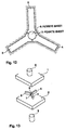
- FIG. 13 shows the structure of the conventional circulator containing the above NRD guide.
- three dielectric strips 3, 4, and 5 are disposed between conductor plates 1 and 2 to form the NRD guide.
- Ferrite sheets 6 and 7 are arranged at the portion where the three dielectric strips are butted together.
- Magnets 8 and 9 are placed on the outer sides of the conductor plates 1 and 2 in such a manner as to sandwich the ferrite sheets 6 and 7.
- a ferrite resonator comprising the ferrite sheets 6 and 7 is excited by an electromagnetic wave which is transmitted through the dielectric strips.
- a DC magnetic field is applied vertically to the surfaces of the ferrite sheets 6 and 7.
- the permeability of the ferrite sheets differs depending on the rotation direction of the high frequency magnetic field, as a result the polarized wave faces rotate, functioning as a circulator.
- a nonreciprocal circuit device including a dielectric wave guide such as the above-described circulator
- the dielectric strips are arranged to extend radially from the center of the circulator. Therefore, dielectric strips of another circuit unit can seldom be linearly connected to the dielectric strips.
- bending of the dielectric strips at some points is indispensable.
- an LSM01 mode which is the main transmission mode, becomes asymmetric with respect to the lateral direction. Thus, the conversion of the LSM01 mode to an LSE01 mode occurs.
- the bent portion is designed so that all the electric power is completely converted to the LSM01 mode at the terminal of the bent portion, there is the problem that the bent portion cannot be formed to have a desired bending angle and radius of curvature. Accordingly, the applicant of the present invention filed Japanese Patent Application No.
- an NRD guide (hereinafter, referred to as a hyper NRD guide) is described in which a groove into which a dielectric strip is to be fitted is formed on a conductor plate so that the cut-off frequency of the LSM01 mode is lower than that of the LSE01 mode in the propagation range of the dielectric wave guide; and in the non-propagation range, the space between the conductor planes of the conductor plates is made narrow so that the propagation can be carried out exclusively in the LSM01 mode.
- a hyper NRD guide a groove into which a dielectric strip is to be fitted is formed on a conductor plate so that the cut-off frequency of the LSM01 mode is lower than that of the LSE01 mode in the propagation range of the dielectric wave guide; and in the non-propagation range, the space between the conductor planes of the conductor plates is made narrow so that the propagation can be carried out exclusively in the LSM01 mode.
- the structure of the hyper NRD guide applied to the circulator is shown in FIG. 11, for example.
- the conductor plates 1 and 2 have grooves 21 and 22 respectively formed on the opposing surfaces thereof.
- the conductor plates 1 and 2 are so assembled that the dielectric strips 3, 4, and 5 and the ferrite sheets 6 and 7 fit into the grooves.
- the ferrite sheets 6 and 7 function as a ferrite resonator, couple a signal propagated in the LSM01 mode along one of the dielectric strips, and simultaneously rotate the polarized wave faces to propagate the signal in the LSM01 mode to another dielectric strip.
- FIG. 12 is an upper plan view of the ferrite sheets 6 and 7 and the dielectric strips 3, 4, and 5 which are fitted into the groove 22 of the conductor plate 2 shown in FIG. 11.
- the grooves 21 and 22 are respectively formed on the conductor plates 1 and 2 and the dielectric strips 3, 4 and 5 and the ferrite sheets 6 and 7 are fitted into the grooves 21 and 22, an electromagnetic field is disturbed on the periphery of the ferrite sheets 6 and 7 if the side walls of the grooves 21 and 22 of the respective conductor plates 1 and 2 are disposed very close to the side faces of the ferrite sheets 6 and 7.
- the ferrite resonator formed of the ferrite sheets 6 and 7 and the dielectric wave guides 3, 4 and 5 are not matched.
- the thicknesses (shown by the arrows of FIG. 12) of the dielectric portions parallel to the tangential directions of the ferrite sheets 6 and 7 are increased, and thereby, spaces are widened between the side faces of the ferrite sheets 6 and 7 and the side walls of the grooves on the respective conductor plates 1 and 2.
- an electromagnetic wave is propagated through the dielectric portions on the periphery of the ferrite sheets 6 and 7, so that the magnetic field coupling of the ferrite sheets 6 and 7 is weakened.
- the circulator having three ports as shown in FIG. 12, for example, not only an electromagnetic wave is propagated from one of the ports to one of the other two ports, but also the electromagnetic wave is leaked to the remaining port. That is, the characteristics of the circulator as a nonreciprocal circuit device deteriorate.
- the foregoing problem is caused not only in the case of the hyper NDR guide but also in a device in which grooves are formed in conductor plates and dielectric strips are arranged in the grooves.
- a nonreciprocal circuit including a dielectric wave guide device which has a structure in which a dielectric strip is fitted into grooves formed on conductor plates, and in which the nonreciprocal characteristics are prevented from being deteriorated, and radio device including the nonreciprocal circuit device.
- a nonreciprocal circuit device which comprises a dielectric strip extending radially from the center in at least two directions, arranged between two conductor plates constituting parallel conductor planes, and a ferrite arranged in the center of the dielectric strip.
- a substance having a lower dielectric constant than the dielectric strip is arranged between at least a side face of the ferrite and the conductor plates adjacent to the side face of the ferrite. Accordingly, matching of the resonance mode of the ferrite and the mode of the dielectric wave guide can be easily achieved, and also, since the dielectric constant on the periphery of the ferrite is reduced, the magnetic filed coupling to the ferrite is not reduced, giving excellent nonreciprocal characteristics.
- concave portions are formed in the centers of the conductor plates, and the substance having a lower dielectric constant than the dielectric strip (for example, a space) is arranged on the periphery of the ferrite. Further, on the conductor plates, are formed the grooves into which the dielectric strip is inserted to a predetermined depth, the width of the dielectric strip is increased in the centers of the conductor plates and in the direction along the parallel conductor planes of the conductor plates, and the substance having a low dielectric constant (for example, a space) is arranged at the widened location and between the side walls of the grooves and the side face of the ferrite.
- radio device which includes the nonreciprocal circuit device as a circulator containing the dielectric wave guide formed of the dielectric strip whereby a transmitting signal and a receiving signal are branched by means of the circulator.
- the radio device includes an isolator comprising the nonreciprocal circuit device in which a predetermined dielectric wave guide is provided with a terminator, whereby the reverse propagation of a signal is stopped by means of the isolator.
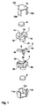
- FIG. 1 is an exploded perspective view of the circulator.
- Opposing surfaces of conductor plates 1 and 2 shown in FIG. 1 constitute conductor planes substantially parallel to each other.
- Grooves 21 and 22 are formed on the opposing surfaces of the two conductor plates 1 and 2, respectively.
- a dielectric strip 3 three dielectric strip portions 3a, 3b, and 3c are integrally formed and extend radially at angular intervals of 120°.
- FIG. 3 is an exploded perspective view of the conductor plates 1 and 2, and the members to be sandwiched between the conductor plates 1 and 2.
- Concave portions are formed on the upper and lower surfaces in the center of the dielectric strip 3.
- Ferrite sheets 6 and 7 are fitted into the concave portions, and are sandwiched between the conductor plates 1 and 2 positioned at the upper and lower sides, respectively, and thereby, three hyper NRD guides, through which signals are propagated in the LSM01 mode, and a ferrite resonator resonating in the HE mode, are formed.
- concave portions for accommodating columnar-shaped magnets 8 and 9 are formed on the outer surfaces of the conductor plates 1 and 2.
- the concave portion 1d is formed on the upper conductor plate 1.
- Magnetic members 10 and 11 have side walls 10a, 10b, and 10c, and 11a, 11b, and 11c, respectively.
- the dielectric strip 3 and the ferrite sheets 6 and 7 are sandwiched between the conductor plates 1 and 2, respectively.
- the magnets 8 and 9 are received in the concave portions of the conductor plates 1 and 2. Further, they are sandwiched between the magnetic members 10 and 11 placed from the outside, respectively, so that these parts are integrated.
- Notches 1a, 1b, and 1c, and 2a, 2b, and 2c are provided in the conductor plates 1 and 2, respectively, at angles of 120°, each notch being disposed between a respective pair of the dielectric strips 3, 4 and 5.
- the side walls of the magnetic members 10 and 11 engage with the corresponding notches.
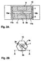
- FIGS. 2A and 2B show illustrations of the assembled circulator of FIG. 1.
- FIG. 2B is an upper plan view of the circulator
- FIG. 2A is a cross-sectional view taken along the line A-A of FIG. 2B.
- the opposing surfaces of the upper and lower conductor plates 1 and 2, respectively, defines the conductor planes.
- the conductor planes and the dielectric strips arranged therebetween form the hyper NRD guide.
- the space between the opposing surfaces of the conductor plates 1 and 2 is set to be narrower than ⁇ /2, where ⁇ represents the wavelength of a millimeter wave which is an electromagnetic wave to be transmitted, and thereby, in the portions of the conductor planes where there are no dielectric strips, the propagation of the electromagnetic wave having a polarized wave face parallel to the conductor planes is blocked. Further, the space between the opposing surfaces of the conductor plates 1 and 2 and the height of the dielectric strip 3 are so set that the cut-off frequency in the LSM01 mode is lower than that in the LSE01 mode.
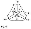
- FIG. 4 is an upper plan view of the circulator when the upper conductor plate 1 is removed.
- the width of the groove 22 provided for the conductor plate 2 is substantially equal to the width of the dielectric strips portions 3a, 3b, and 3c.
- spaces 12, as a medium having a lower dielectric constant than the dielectric strip 3 are formed between the side walls of the groove 22 and the side-face of the ferrite sheet 7.
- the matching between the resonance mode of the ferrite sheet and the mode of the dielectric wave guide can be easily achieved, and moreover, since the dielectric constant at the periphery of the ferrite sheet is reduced, excellent nonreciprocal characteristics can be attained without weakening the magnetic field coupling to the ferrite sheet.
- FIG. 5 shows the structure of a circulator according to a second embodiment of the present invention.
- the dielectric strip described in the first embodiment has an integrated three-forked shape.
- three independent, separate dielectric strips 3, 4, and 5 are employed, arranged to extend radially from the center in three directions at angular intervals of 120°.
- a dielectric spacer 14 is used, and on the upper and lower sides of the spacer 14, the ferrite sheets 6 and 7 are fixed, respectively. Also in this case, spaces are provided between the side walls of grooves of the conductor plates 1 and 2 and the side faces of the ferrite sheets 6 and 7, respectively. Spaces 12 are formed on the conductor plate 2, and similar spaces are also formed on the conductor plate 1.
- FIGS. 6A to 6C show illustrations of other possible shapes of the space 12.
- the spaces form substantially rectangular shapes in plan view.
- the spaces form triangular shapes.
- the spaces form shapes defined by the combination of a curved line with a straight line.
- other shapes of the space can be used. In any case, a distance between the periphery of the ferrite sheets 6 and 7 and the conductor plates is ensured, and moreover, the propagation of an electromagnetic wave at the periphery of the ferrite sheets 6 and 7 can be inhibited. Therefore, excellent nonreciprocal circuit characteristics can be attained.
- FIGS. 7A and 7B show illustrations of the structure of a circulator according to another embodiment of the present invention.
- FIG. 7B is an upper plan view of the circulator when the upper conductor plate is removed.
- FIG. 7A is a cross-sectional view taken along the line A-A of FIG. 7B.
- concave portions 13 are formed in the centers of the conductor plates 1 and 2, that is, a space is formed on the periphery of each of the ferrite sheets 6 and 7.
- FIGS. 8A and 8B a four-port nonreciprocal circuit device including a dielectric wave guide may be formed.
- FIG. 8A is an upper plan view of the four-port nonreciprocal circuit device including a dielectric wave guide when the upper conductor plate is removed.
- FIG. 8B is an illustration of an isolator formed by using the circuit device.
- cross-shaped grooves and spaces 12 are formed on the conductor plate 2.
- the ferrite sheets are fixed to the upper and lower surfaces in the center of a cross-shaped dielectric strip composed of the dielectric strip portions 3a, 3b, 3c, and 3d.
- the dielectric strip is fitted into the groove of the conductor plate 2.
- the upper side of the conductor plate 2 having the dielectric strip fitted into the groove is covered with a conductor plate having the same shape and size as the conductor plate 2, whereby a four-port nonreciprocal circuit device including a dielectric wave guide is formed. If an input signal from one of the dielectric wave guides, which extends radially from the center of the ferrite sheet is output to the adjacent dielectric wave guide in the counterclockwise direction, that is, an input signal from one of the ports is output to the neighboring port on the right, the dielectric wave guide connects the port #1 and the port #2, and terminators are connected to each of the other two ports #3 and #4, as shown in FIG. 8B. Thus, the input signal from the port #1 is output through the port #2.
- the four-port nonreciprocal circuit device including a dielectric wave guide as described above, in which two of the dielectric strips are arranged in a perpendicular configuration, is advantageous in that the circuit configuration of the dielectric wave guide can be easily achieved.
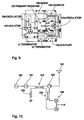
- FIG. 9 is a plan view of the whole of the millimeter wave radar module when the upper conductor plate is removed.
- FIG. 10 is its equivalent circuit diagram.
- the module is mainly composed of an oscillator 100, an isolator 101, a coupler 102, a circulator 104, a coupler 105, a mixer 106, and a primary radiator 107.
- the respective units are connected through an NRD guide as a transmission line.
- the oscillator 100 is provided with a Gunn diode and a varactor diode, and outputs an oscillation signal to the input port of the isolator 101.
- the isolator 101 comprises a circulator, and a terminator 21 connected to the port of the circulator through which the reflected signal from the circulator is output.
- the circulator has a structure according to any one of the first through third embodiments.
- the coupler 102 including two dielectric strips disposed close to each other extracts the Lo (local) signal.
- the circulator 104 outputs a transmission signal to the primary radiator 107 side, and outputs a receiving signal from the primary radiator 107 to the coupler 105.
- the coupler 105 couples the receiving signal with the Lo signal to apply two necessary signals to the mixer 106.
- the mixer 106 mixes the two signals by a balanced-type method to obtain an IF (intermediate frequency) signal.
- the controller of the above-described millimeter wave radar module controls the oscillation frequency of the oscillator 100 by an FM-CW system, and also, signal-processes the IF signal to determine a distance to a detection object and a velocity relative to the detection object.
- the space between the opposing surfaces of the conductor plates is set to be less than half the wavelength of the millimeter wave, and thereby, the propagation of an electromagnetic wave is cut off in the portions of the conductor plates where there are no dielectric strips. Further, the space between the opposing surfaces of the conductor plates and the size of the dielectric strip are so set that the cut-off frequency in the LSM01 mode is lower than that in the LSE01 mode.
- the dielectric wave guide is not limited to the hyper NRD guide and the NRD guide.
- the three and four port circulators are described.
- the circulator is not limited to the three and four port circulators.
- the present invention can be applied to a device in which ferromagnetic sheets are arranged substantially parallel to the conductor planes and adjacent to the planes of the dielectric strip substantially in contact with the conductor plane, so that the device has non-reciprocal circuit characteristics obtained by utilization of its tensor permeability.
- the ferrite sheets are arranged nearly on the planes of the dielectric strip which are in contact with the upper and lower conductor sheets.
- the ferrite sheet may be arranged on only one of the planes of the dielectric strip.
- the ferrite sheet does not need to have a disk shape, and may have a polygonal shape, for example. Further, a columnar-shape ferrite may be used.
- the matching of the resonance mode of the ferrite with the mode of the dielectric wave guide can be easily achieved.
- the dielectric constant at the periphery of the ferrite is reduced, the magnetic field coupling to the ferrite is prevented from weakening, and excellent nonreciprocal characteristics can be attained.
- the branching of a transmitting signal and a receiving signal are carried out by means of the circulator containing the dielectric wave guide and having excellent nonreciprocal characteristics. Accordingly, radio device such as a miniaturized millimeter radar containing the dielectric wave guide can be easily formed.
- the reverse propagation of a signal is stopped by means of the isolator containing the dielectric wave guide and having excellent nonreciprocal circuit characteristics.
- a return signal to an oscillator for example can be positively stopped. Radio equipment with excellent characteristics can be easily formed.
Landscapes
- Waveguides (AREA)
- Non-Reversible Transmitting Devices (AREA)
- Waveguide Switches, Polarizers, And Phase Shifters (AREA)
Applications Claiming Priority (2)
| Application Number | Priority Date | Filing Date | Title |
|---|---|---|---|
| JP22567098A JP3230492B2 (ja) | 1998-08-10 | 1998-08-10 | 誘電体線路非可逆回路素子および無線装置 |
| JP22567098 | 1998-08-10 |
Publications (2)
| Publication Number | Publication Date |
|---|---|
| EP0980110A2 true EP0980110A2 (fr) | 2000-02-16 |
| EP0980110A3 EP0980110A3 (fr) | 2001-08-22 |
Family
ID=16832951
Family Applications (1)
| Application Number | Title | Priority Date | Filing Date |
|---|---|---|---|
| EP99114855A Pending EP0980110A3 (fr) | 1998-08-10 | 1999-07-29 | Dispositif de circuit non réciproque avec guide d' onde diélectrique et appareil radio l' utilisant |
Country Status (6)
| Country | Link |
|---|---|
| US (1) | US6359526B1 (fr) |
| EP (1) | EP0980110A3 (fr) |
| JP (1) | JP3230492B2 (fr) |
| KR (1) | KR100327533B1 (fr) |
| CN (1) | CN1133229C (fr) |
| MY (1) | MY121801A (fr) |
Families Citing this family (5)
| Publication number | Priority date | Publication date | Assignee | Title |
|---|---|---|---|---|
| KR100352488B1 (ko) * | 2000-11-24 | 2002-09-11 | 삼성전기주식회사 | 비가역 회로소자의 가네트 페라이트 결합용 지그 |
| JP3800117B2 (ja) * | 2001-04-26 | 2006-07-26 | 株式会社村田製作所 | 非可逆回路素子 |
| CN104282973A (zh) * | 2014-10-13 | 2015-01-14 | 世达普(苏州)通信设备有限公司 | 集成屏蔽盖波导隔离器 |
| CN111725597B (zh) * | 2019-03-18 | 2021-04-20 | 华为技术有限公司 | 介质传输线耦合器、介质传输线耦合组件及网络设备 |
| JP7826943B2 (ja) * | 2020-12-28 | 2026-03-10 | 戸田工業株式会社 | 帯状フェライトシート並びにそれを用いたアンテナ装置及びケーブル |
Family Cites Families (11)
| Publication number | Priority date | Publication date | Assignee | Title |
|---|---|---|---|---|
| JPS5577203A (en) * | 1978-12-05 | 1980-06-10 | Oki Electric Ind Co Ltd | Strip line type circulator |
| JPS5586203A (en) * | 1978-12-22 | 1980-06-28 | Nec Corp | Unreversible circuit |
| JPS5591203A (en) * | 1978-12-28 | 1980-07-10 | Nec Corp | Waveguide non-reversible circuit |
| US4415871A (en) * | 1981-10-13 | 1983-11-15 | The United States Of America As Represented By The Secretary Of The Army | Dielectric waveguide circulator |
| US4446448A (en) * | 1982-08-13 | 1984-05-01 | The United States Of America As Represented By The Secretary Of The Army | Biasing magnet holder-tuning cap for dielectric waveguide circulator |
| JPS59147301U (ja) * | 1983-03-23 | 1984-10-02 | 三菱電機株式会社 | 導波管形サ−キユレ−タ |
| JP3220966B2 (ja) * | 1994-08-30 | 2001-10-22 | 株式会社村田製作所 | 非放射性誘電体線路部品 |
| JPH08181510A (ja) * | 1994-10-25 | 1996-07-12 | Honda Motor Co Ltd | Nrdガイド回路の組立方法およびnrdガイド回路 |
| JP3125974B2 (ja) * | 1994-10-25 | 2001-01-22 | 本田技研工業株式会社 | Nrdガイド回路、レーダモジュールおよびレーダ装置 |
| JPH09186507A (ja) | 1995-12-28 | 1997-07-15 | Nissan Motor Co Ltd | Nrdガイド用サーキュレータ |
| JP3018987B2 (ja) * | 1996-07-08 | 2000-03-13 | 株式会社村田製作所 | 誘電体線路集積回路 |
-
1998
- 1998-08-10 JP JP22567098A patent/JP3230492B2/ja not_active Expired - Lifetime
-
1999
- 1999-07-29 EP EP99114855A patent/EP0980110A3/fr active Pending
- 1999-07-30 MY MYPI99003273A patent/MY121801A/en unknown
- 1999-08-09 KR KR1019990032548A patent/KR100327533B1/ko not_active Expired - Lifetime
- 1999-08-10 CN CN99111793A patent/CN1133229C/zh not_active Expired - Lifetime
- 1999-08-10 US US09/371,365 patent/US6359526B1/en not_active Expired - Lifetime
Also Published As
| Publication number | Publication date |
|---|---|
| CN1133229C (zh) | 2003-12-31 |
| KR100327533B1 (ko) | 2002-03-14 |
| JP3230492B2 (ja) | 2001-11-19 |
| EP0980110A3 (fr) | 2001-08-22 |
| US6359526B1 (en) | 2002-03-19 |
| CN1244736A (zh) | 2000-02-16 |
| MY121801A (en) | 2006-02-28 |
| JP2000059110A (ja) | 2000-02-25 |
| KR20000017189A (ko) | 2000-03-25 |
Similar Documents
| Publication | Publication Date | Title |
|---|---|---|
| US5867120A (en) | Transmitter-receiver | |
| EP0820114B1 (fr) | Circuit de ligne diélectrique multicouches | |
| US20020021196A1 (en) | Dielectric waveguide | |
| EP0767507A1 (fr) | Guide d'onde diélectrique | |
| JP3303757B2 (ja) | 非放射性誘電体線路部品およびその集積回路 | |
| CA2256283C (fr) | Guide d'ondes dielectrique non radiatif comprenant une partie pour la conversion de ligne entre differents types de guides d'ondes dielectriques non radiatifs | |
| US6359526B1 (en) | Nonreciprocal circuit device including dielectric wave guide and a lower dielectric constant medium | |
| EP0855755B1 (fr) | Croisement pour lignes diélectriques | |
| US6931246B2 (en) | Line coupling structure, mixer, and receiving/transmitting apparatus comprised of suspended line and dielectric waveguide | |
| US6496080B1 (en) | Dielectric waveguide nonreciprocal circuit device with a non-interfering magnetic member support | |
| US6445355B2 (en) | Non-radiative hybrid dielectric line transition and apparatus incorporating the same | |
| KR100319811B1 (ko) | 비가역 회로소자, 비가역 회로장치 및 이들을 사용하는송수신기 | |
| JP3259637B2 (ja) | 送受信装置 | |
| US6208218B1 (en) | Nonreciprocal circuit device including dielectric wave guide, dielectric wave guide device and radio device | |
| KR100337167B1 (ko) | 유전체 필터, 송수신 공용기 및 통신기 | |
| JP3386006B2 (ja) | 誘電体線路非可逆回路素子、誘電体線路装置および無線装置 | |
| JP2003188764A (ja) | 送受信装置およびレーダ装置 | |
| JP2000165113A (ja) | 高周波回路装置および無線装置 | |
| JP2002124804A (ja) | 非可逆回路素子、無線装置および非可逆回路素子の周波数調整方法 |
Legal Events
| Date | Code | Title | Description |
|---|---|---|---|
| PUAI | Public reference made under article 153(3) epc to a published international application that has entered the european phase |
Free format text: ORIGINAL CODE: 0009012 |
|
| 17P | Request for examination filed |
Effective date: 19990729 |
|
| AK | Designated contracting states |
Kind code of ref document: A2 Designated state(s): AT BE CH CY DE DK ES FI FR GB GR IE IT LI LU MC NL PT SE |
|
| AX | Request for extension of the european patent |
Free format text: AL;LT;LV;MK;RO;SI |
|
| PUAL | Search report despatched |
Free format text: ORIGINAL CODE: 0009013 |
|
| AK | Designated contracting states |
Kind code of ref document: A3 Designated state(s): AT BE CH CY DE DK ES FI FR GB GR IE IT LI LU MC NL PT SE |
|
| AX | Request for extension of the european patent |
Free format text: AL;LT;LV;MK;RO;SI |
|
| AKX | Designation fees paid |
Free format text: DE FR GB |
|
| 17Q | First examination report despatched |
Effective date: 20070910 |
|
| RAP1 | Party data changed (applicant data changed or rights of an application transferred) |
Owner name: MURATA MANUFACTURING CO., LTD. |
|
| STAA | Information on the status of an ep patent application or granted ep patent |
Free format text: STATUS: EXAMINATION IS IN PROGRESS |