EP0980169A2 - Tranmsission d'informations par codage manchester différentielle et modulation par déplacement de phase - Google Patents
Tranmsission d'informations par codage manchester différentielle et modulation par déplacement de phase Download PDFInfo
- Publication number
- EP0980169A2 EP0980169A2 EP99440216A EP99440216A EP0980169A2 EP 0980169 A2 EP0980169 A2 EP 0980169A2 EP 99440216 A EP99440216 A EP 99440216A EP 99440216 A EP99440216 A EP 99440216A EP 0980169 A2 EP0980169 A2 EP 0980169A2
- Authority
- EP
- European Patent Office
- Prior art keywords
- signal
- phase
- output
- data
- differential manchester
- Prior art date
- Legal status (The legal status is an assumption and is not a legal conclusion. Google has not performed a legal analysis and makes no representation as to the accuracy of the status listed.)
- Granted
Links
Images
Classifications
-
- H—ELECTRICITY
- H04—ELECTRIC COMMUNICATION TECHNIQUE
- H04L—TRANSMISSION OF DIGITAL INFORMATION, e.g. TELEGRAPHIC COMMUNICATION
- H04L27/00—Modulated-carrier systems
- H04L27/18—Phase-modulated carrier systems, i.e. using phase-shift keying
- H04L27/22—Demodulator circuits; Receiver circuits
-
- H—ELECTRICITY
- H04—ELECTRIC COMMUNICATION TECHNIQUE
- H04L—TRANSMISSION OF DIGITAL INFORMATION, e.g. TELEGRAPHIC COMMUNICATION
- H04L25/00—Baseband systems
- H04L25/38—Synchronous or start-stop systems, e.g. for Baudot code
- H04L25/40—Transmitting circuits; Receiving circuits
- H04L25/49—Transmitting circuits; Receiving circuits using code conversion at the transmitter; using predistortion; using insertion of idle bits for obtaining a desired frequency spectrum; using three or more amplitude levels ; Baseband coding techniques specific to data transmission systems
- H04L25/4904—Transmitting circuits; Receiving circuits using code conversion at the transmitter; using predistortion; using insertion of idle bits for obtaining a desired frequency spectrum; using three or more amplitude levels ; Baseband coding techniques specific to data transmission systems using self-synchronising codes, e.g. split-phase codes
-
- H—ELECTRICITY
- H04—ELECTRIC COMMUNICATION TECHNIQUE
- H04L—TRANSMISSION OF DIGITAL INFORMATION, e.g. TELEGRAPHIC COMMUNICATION
- H04L27/00—Modulated-carrier systems
- H04L27/18—Phase-modulated carrier systems, i.e. using phase-shift keying
Definitions
- the invention relates to a method for transmitting Information using phase modulation, especially 2-PSK.
- 2-PSK is one digital phase modulation with two different states of the in the Phase modulated signal. These methods are well known and the Those skilled in the art know that the demodulated signal is not unique and therefore special measures to ensure uniqueness are taken must, namely a phase recovery must be carried out. After demodulation it is not known whether a bit has the value 0 or has 1. With 2-PSK it is only known that the demodulated signal is composed of bits with two different values. For the production The unmodulated high-frequency signal can, for example, be unique be transferred with. Another solution can be that at least at the start of a message transmission one of the Known bit sequence is received on the receiving side, so that it is on the Receiving side is possible, so the polarity of the demodulated bits set that exactly this bit sequence results.
- the invention has for its object a method and to specify a system in which the recipient's effort for Phase demodulation is reduced.
- This task is done in the process solved according to the invention in that the differential Manchester code together with a modified phase modulation transmission method, preferably 2-PSK method, is used in which is a polarity recovery in contrast to the state of the Technology is not made.
- a device for polarity recovery not required and not available.
- the invention is not limited to that Differential manchester code exactly in the form in which it is defined is used. Rather, any code is applicable to the invention that Similar to the code just mentioned, regardless of the phase position always allows the distinction between bits 0 and 1 in a clear manner. For example, in the case of the differential Manchester code Meaning of bits 0 and 1 are interchanged; also one of those modified code would be applicable to the invention.
- Method of the system according to the invention is a pilot tone by means of transferred method according to the invention, wherein it is advantageous that this pilot tone (which is known for setting a certain level of the Signal used on the receiving side), a message transmitted can.
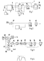
- a transmitting part 1 has a data processor 2 whose clock is controlled by a quartz crystal 4.
- data is generated that the data processor 2nd be fed.
- the data in accordance with the Differential Manchester code encoded data and converted to one Data output 8 output.
- a clock signal is received by processor 2 a clock output 10 output.
- the data from data output 8 are re-clocked in a first flip-flop 12 (FF1) to convert them into a bring exact timing.
- the processor clock from clock output 10 is divided by a clock divider 14 in the example in a ratio of 8: 1 (this Divisional relationship has no necessary connection with the usual representation of messages in the form of bytes, each 8 bits exhibit).
- the output signal of the first flip-flop 12 becomes one of the two inputs of an exclusive-OR circuit 16 (EXOR) supplied, and the other input of this circuit 16, the output signal of the Clock divider 14 supplied.
- the exclusive OR circuit 16 causes a controlled by the data output of the first flip-flop 12 Inverting the clock from the output of the clock divider 14, in each case Zero crossing of the clock.
- the output signal of the exclusive-OR circuit 16 is phase modulated with two 180 ° different ones Phases, there is 2-PSK.
- the output signal of the exclusive-OR circuit 16 is fed to a second flip-flop 18 (FF2), in which Switching peaks that are generated in real exclusive-OR circuits, be eliminated. That at the data output 20 of the second flip-flop 18 appearing signal is the technically corrected for switching peaks further processable, in particular transmissible via a data channel phase modulated signal.
- FF2 flip-flop 18
- the received is too demodulating phase-modulated signal is first a comparator 40 fed, which may be out of the course of the transfer smoothed and rounded phase-modulated signal again exact Generated pulses with constant amplitude.
- a device 42 for Clock recovery wins the comparator 40 from there Signal leaving the output a clock signal with a duty cycle of 1: 1. That the Comparator 40 leaving data signal and the device 42nd Exiting clock signals are an exclusive-OR circuit 44 at the fed to both inputs, and this circuit causes one Demodulation of the phase-modulated signal.
- the output of the exclusive-or circuit 44 is connected to the input of a low pass 46 whose output is the demodulated data signal, the output signal at the output 8 of the processor 2 corresponds to FIG. 1 or is inverted is available.
- Has the clock signal at the output of device 42 the clock frequency, as at the output of the clock divider 14 of the arrangement 1 is available.
- the detailed block diagram of FIG. 3 arrives the phase-modulated signal to be demodulated to the input of a Actuator 60, the gain of which is adjustable.
- the output 62 of the The servo amplifier 60 is connected to the input via a bandpass 64 Rectifier assembly 66 connected to the output of one of the Amplitude at the output 62 of the servo amplifier 60 proportional signal is issued.
- the exit of the Control amplifier 68 has a control input of the control amplifier 60 connected and changed its reinforcement. In this way, one Regulation made that ensures that the output signal of the Rectifier arrangement 66 is exactly the same as the reference voltage Uref. Then the output signal of the control amplifier 60 has that for the further Machining required and desired amplitude.
- the Exclusive-OR circuit 84 a low-pass filter, which here is the reference number 94 3, and this becomes the low pass 94 leaving signal still by a flip-flop 96, the clock input the Clock signal is supplied from the output of the clock divider 92, peak-free clocked.
- Fig. 3 it is also shown that the input of the Actuator 60 not only the above-mentioned phase-modulated signal (PSK) is supplied, but it is also a useful signal, symbolized by the letters TV, which in the example is a Signal in the frequency range from 5 MHz to 70 MHz for the upstream channel acts (cablephone), fed.
- This signal is at the output of the Adjustment amplifier 62 removed, if necessary, by a high pass 100.
- the Actuating amplifier 62 amplifies the useful signal TV in the same way as that phase modulated signal.
- the latter phase-modulated signal provides therefore represents a pilot tone in the exemplary embodiment, of which is known what amplitude it must be amplified at the receiving end, so that too Useful signal receives the amplitude required for its further use.
- Fig. 4 shows the representation of bits 0 and 1 according to the Differential Manchester code.
- Bit 0 is characterized in that there is a transition in the middle of the bit. This distinguishes bit 1 that there is no transition in the middle of the bit.
- bit boundaries exist. As can be easily recognized, it works a phase reversal of bit 0 or bit 1 does not cause any swapping of the bits themselves, because even after the phase reversal at bit 0 the mentioned transition is present, but not at bit 1.
- other encodings can be used, in which this last described property is present.
- the receiving device according to the invention or Demodulation device on any device to a certain Specify the phase position for the demodulated signal.
- the method according to the invention therefore enables simplification of the receiving circuit compared to conventional Phase modulation method in which the phase position of the transmitted Signal must be restored.
Landscapes
- Engineering & Computer Science (AREA)
- Computer Networks & Wireless Communication (AREA)
- Signal Processing (AREA)
- Physics & Mathematics (AREA)
- Spectroscopy & Molecular Physics (AREA)
- Digital Transmission Methods That Use Modulated Carrier Waves (AREA)
- Dc Digital Transmission (AREA)
- Optical Communication System (AREA)
- Burglar Alarm Systems (AREA)
Applications Claiming Priority (2)
| Application Number | Priority Date | Filing Date | Title |
|---|---|---|---|
| DE19835952 | 1998-08-08 | ||
| DE19835952A DE19835952A1 (de) | 1998-08-08 | 1998-08-08 | Verfahren und System zur Informationsübertragung mittels Phasenmodulation |
Publications (3)
| Publication Number | Publication Date |
|---|---|
| EP0980169A2 true EP0980169A2 (fr) | 2000-02-16 |
| EP0980169A3 EP0980169A3 (fr) | 2002-09-11 |
| EP0980169B1 EP0980169B1 (fr) | 2004-02-04 |
Family
ID=7876914
Family Applications (1)
| Application Number | Title | Priority Date | Filing Date |
|---|---|---|---|
| EP99440216A Expired - Lifetime EP0980169B1 (fr) | 1998-08-08 | 1999-07-29 | Transmission d'information par codage manchester différentiel et modulation par déplacement de phase |
Country Status (5)
| Country | Link |
|---|---|
| US (1) | US6498818B1 (fr) |
| EP (1) | EP0980169B1 (fr) |
| AT (1) | ATE259126T1 (fr) |
| CA (1) | CA2279585A1 (fr) |
| DE (2) | DE19835952A1 (fr) |
Family Cites Families (9)
| Publication number | Priority date | Publication date | Assignee | Title |
|---|---|---|---|---|
| JPS5946143B2 (ja) * | 1976-04-16 | 1984-11-10 | パイオニア株式会社 | 双方向catvシステムにおける伝送確認方法および装置 |
| US4281412A (en) * | 1979-07-05 | 1981-07-28 | Cincinnati Electronics Corporation | Method of and apparatus for transmitting and recovering offset QPSK modulated data |
| US4507794A (en) * | 1983-05-04 | 1985-03-26 | Jones Stephen K | Filtered Manchester Coded PSK transmission system |
| US4562415A (en) * | 1984-06-22 | 1985-12-31 | Motorola, Inc. | Universal ultra-precision PSK modulator with time multiplexed modes of varying modulation types |
| JPH073966B2 (ja) * | 1985-08-29 | 1995-01-18 | パイオニア株式会社 | 放送受信装置 |
| US4912730A (en) * | 1988-10-03 | 1990-03-27 | Harris Corporation | High speed reception of encoded data utilizing dual phase resynchronizing clock recovery |
| KR930005646B1 (ko) * | 1990-10-08 | 1993-06-23 | 삼성전자 주식회사 | 평탄한 엔벨로프 특성을 갖는 bpsk 변조회로 |
| KR930012023B1 (ko) * | 1991-01-25 | 1993-12-23 | 삼성전관 주식회사 | 평탄한 엔벨로프 특성을 갖는 bpsk 변조회로 |
| DE4223132A1 (de) * | 1992-07-14 | 1994-01-20 | Deutsche Aerospace | Verfahren zur Schrittakt-Regeneration bei der Demodulation von digital modulierten Signalen und Anordnung zum Ausführen des Verfahrens |
-
1998
- 1998-08-08 DE DE19835952A patent/DE19835952A1/de not_active Withdrawn
-
1999
- 1999-07-29 AT AT99440216T patent/ATE259126T1/de not_active IP Right Cessation
- 1999-07-29 EP EP99440216A patent/EP0980169B1/fr not_active Expired - Lifetime
- 1999-07-29 DE DE59908449T patent/DE59908449D1/de not_active Expired - Fee Related
- 1999-08-03 CA CA002279585A patent/CA2279585A1/fr not_active Abandoned
- 1999-08-06 US US09/369,809 patent/US6498818B1/en not_active Expired - Fee Related
Also Published As
| Publication number | Publication date |
|---|---|
| ATE259126T1 (de) | 2004-02-15 |
| EP0980169A3 (fr) | 2002-09-11 |
| DE19835952A1 (de) | 2000-02-10 |
| EP0980169B1 (fr) | 2004-02-04 |
| CA2279585A1 (fr) | 2000-02-08 |
| DE59908449D1 (de) | 2004-03-11 |
| US6498818B1 (en) | 2002-12-24 |
Similar Documents
| Publication | Publication Date | Title |
|---|---|---|
| DE2648977C3 (de) | Demodulator für differentiell phasencodierte Digitaldaten | |
| DE2245189C3 (de) | Vorrichtung zur Übertragung eines restseitenbandträgermodulierten Mehrpegelsignals und eines Synchronisier-Pilotsignals | |
| DE2512161C2 (de) | Digitaler Frequenzverschiebungs-Demodulator | |
| DE2221146C3 (de) | Schaltungsanordnung zum Übertragen eines Mehrpegelsignalzuges mit darin eingesetzten Pilotsignalen | |
| DE1213882B (de) | Verfahren und Schaltungsanordnung zum UEbertragen von Daten in Form einer binaer-codierten Impulsfolge | |
| DE2427225C3 (de) | Schaltungsanordnung zur Demodulation digitaler Information | |
| EP0304799B1 (fr) | Dispositif pour démoduler un signal biphasé | |
| CH620068A5 (fr) | ||
| EP0115327B1 (fr) | Décodeur CMI | |
| DE1437169B2 (de) | Verfahren zur schnelluebertragung von daten im restseiten bandverfahren die nach einem binaeren vode oder nach einem mehrpegelcode verschluesselt sind | |
| DE3015216C2 (de) | Anordnung zum Überprüfen der Synchronisation eines Empfängers | |
| DE2253015A1 (de) | Breitbanddiskriminator | |
| DE2242550A1 (de) | Elektrische codier- und decodiervorrichtung | |
| DE3834865A1 (de) | Verfahren und schaltung zur ableitung von h- und v-frequenten synchronimpulsen | |
| DE69317200T2 (de) | Datenverarbeitungsschaltung | |
| DE2557922B2 (de) | Verfahren zum Komprimieren von Faksimiledaten und Vorrichtung zu seiner Durchführung | |
| DE2651043C3 (de) | Empfänger für synchrone Signale mit doppelter phasenverriegelter Schleife | |
| EP0980169B1 (fr) | Transmission d'information par codage manchester différentiel et modulation par déplacement de phase | |
| DE1294430B (de) | Schaltungsanordnung zum Empfang amplitudenmodulierter Viel-stufen-Datensignale mit unterdruecktem Traeger | |
| DE2906886C2 (de) | Schaltungsanordnung zur Schrittakt-Gewinnung | |
| DE2525533C2 (de) | Einrichtung zum Decodieren eines Code | |
| DE3131845A1 (de) | Verfahren zum erzeugen und erfassen digitaler signale beliebiger zeichencodierung | |
| DE2744942A1 (de) | Nachrichtenuebertragungssystem mit einer sende- und empfangseinrichtung | |
| DE4433779C2 (de) | Phasendetektor für die Steuerung der Rückgewinnung eines Trägersignals | |
| DE1537016B2 (de) | Verfahren und schaltungsanordnung zur uebertragung von binaeren eingangsdaten mittels einer modifizierten duobinae ren traegermodulation |
Legal Events
| Date | Code | Title | Description |
|---|---|---|---|
| PUAI | Public reference made under article 153(3) epc to a published international application that has entered the european phase |
Free format text: ORIGINAL CODE: 0009012 |
|
| AK | Designated contracting states |
Kind code of ref document: A2 Designated state(s): AT BE CH CY DE DK ES FI FR GB GR IE IT LI LU MC NL PT SE |
|
| AX | Request for extension of the european patent |
Free format text: AL;LT;LV;MK;RO;SI |
|
| PUAL | Search report despatched |
Free format text: ORIGINAL CODE: 0009013 |
|
| AK | Designated contracting states |
Kind code of ref document: A3 Designated state(s): AT BE CH CY DE DK ES FI FR GB GR IE IT LI LU MC NL PT SE |
|
| AX | Request for extension of the european patent |
Free format text: AL;LT;LV;MK;RO;SI |
|
| 17P | Request for examination filed |
Effective date: 20020917 |
|
| 17Q | First examination report despatched |
Effective date: 20021022 |
|
| AKX | Designation fees paid |
Designated state(s): AT BE CH CY DE DK ES FI FR GB GR IE IT LI LU MC NL PT SE |
|
| GRAP | Despatch of communication of intention to grant a patent |
Free format text: ORIGINAL CODE: EPIDOSNIGR1 |
|
| GRAS | Grant fee paid |
Free format text: ORIGINAL CODE: EPIDOSNIGR3 |
|
| GRAA | (expected) grant |
Free format text: ORIGINAL CODE: 0009210 |
|
| AK | Designated contracting states |
Kind code of ref document: B1 Designated state(s): AT BE CH CY DE DK ES FI FR GB GR IE IT LI LU MC NL PT SE |
|
| PG25 | Lapsed in a contracting state [announced via postgrant information from national office to epo] |
Ref country code: NL Free format text: LAPSE BECAUSE OF FAILURE TO SUBMIT A TRANSLATION OF THE DESCRIPTION OR TO PAY THE FEE WITHIN THE PRESCRIBED TIME-LIMIT Effective date: 20040204 Ref country code: IE Free format text: LAPSE BECAUSE OF FAILURE TO SUBMIT A TRANSLATION OF THE DESCRIPTION OR TO PAY THE FEE WITHIN THE PRESCRIBED TIME-LIMIT Effective date: 20040204 Ref country code: FR Free format text: LAPSE BECAUSE OF FAILURE TO SUBMIT A TRANSLATION OF THE DESCRIPTION OR TO PAY THE FEE WITHIN THE PRESCRIBED TIME-LIMIT Effective date: 20040204 Ref country code: FI Free format text: LAPSE BECAUSE OF FAILURE TO SUBMIT A TRANSLATION OF THE DESCRIPTION OR TO PAY THE FEE WITHIN THE PRESCRIBED TIME-LIMIT Effective date: 20040204 Ref country code: CY Free format text: LAPSE BECAUSE OF FAILURE TO SUBMIT A TRANSLATION OF THE DESCRIPTION OR TO PAY THE FEE WITHIN THE PRESCRIBED TIME-LIMIT Effective date: 20040204 |
|
| REG | Reference to a national code |
Ref country code: GB Ref legal event code: FG4D Free format text: NOT ENGLISH |
|
| REG | Reference to a national code |
Ref country code: CH Ref legal event code: EP |
|
| GBT | Gb: translation of ep patent filed (gb section 77(6)(a)/1977) |
Effective date: 20040204 |
|
| REG | Reference to a national code |
Ref country code: IE Ref legal event code: FG4D Free format text: GERMAN |
|
| REF | Corresponds to: |
Ref document number: 59908449 Country of ref document: DE Date of ref document: 20040311 Kind code of ref document: P |
|
| PG25 | Lapsed in a contracting state [announced via postgrant information from national office to epo] |
Ref country code: SE Free format text: LAPSE BECAUSE OF FAILURE TO SUBMIT A TRANSLATION OF THE DESCRIPTION OR TO PAY THE FEE WITHIN THE PRESCRIBED TIME-LIMIT Effective date: 20040504 Ref country code: GR Free format text: LAPSE BECAUSE OF FAILURE TO SUBMIT A TRANSLATION OF THE DESCRIPTION OR TO PAY THE FEE WITHIN THE PRESCRIBED TIME-LIMIT Effective date: 20040504 Ref country code: DK Free format text: LAPSE BECAUSE OF FAILURE TO SUBMIT A TRANSLATION OF THE DESCRIPTION OR TO PAY THE FEE WITHIN THE PRESCRIBED TIME-LIMIT Effective date: 20040504 |
|
| PG25 | Lapsed in a contracting state [announced via postgrant information from national office to epo] |
Ref country code: ES Free format text: LAPSE BECAUSE OF FAILURE TO SUBMIT A TRANSLATION OF THE DESCRIPTION OR TO PAY THE FEE WITHIN THE PRESCRIBED TIME-LIMIT Effective date: 20040515 |
|
| PG25 | Lapsed in a contracting state [announced via postgrant information from national office to epo] |
Ref country code: LU Free format text: LAPSE BECAUSE OF NON-PAYMENT OF DUE FEES Effective date: 20040729 Ref country code: GB Free format text: LAPSE BECAUSE OF NON-PAYMENT OF DUE FEES Effective date: 20040729 Ref country code: AT Free format text: LAPSE BECAUSE OF NON-PAYMENT OF DUE FEES Effective date: 20040729 |
|
| PG25 | Lapsed in a contracting state [announced via postgrant information from national office to epo] |
Ref country code: MC Free format text: LAPSE BECAUSE OF NON-PAYMENT OF DUE FEES Effective date: 20040731 Ref country code: LI Free format text: LAPSE BECAUSE OF NON-PAYMENT OF DUE FEES Effective date: 20040731 Ref country code: CH Free format text: LAPSE BECAUSE OF NON-PAYMENT OF DUE FEES Effective date: 20040731 Ref country code: BE Free format text: LAPSE BECAUSE OF NON-PAYMENT OF DUE FEES Effective date: 20040731 |
|
| NLV1 | Nl: lapsed or annulled due to failure to fulfill the requirements of art. 29p and 29m of the patents act | ||
| REG | Reference to a national code |
Ref country code: IE Ref legal event code: FD4D |
|
| PLBE | No opposition filed within time limit |
Free format text: ORIGINAL CODE: 0009261 |
|
| STAA | Information on the status of an ep patent application or granted ep patent |
Free format text: STATUS: NO OPPOSITION FILED WITHIN TIME LIMIT |
|
| 26N | No opposition filed |
Effective date: 20041105 |
|
| EN | Fr: translation not filed | ||
| BERE | Be: lapsed |
Owner name: *ALCATEL Effective date: 20040731 |
|
| PG25 | Lapsed in a contracting state [announced via postgrant information from national office to epo] |
Ref country code: DE Free format text: LAPSE BECAUSE OF NON-PAYMENT OF DUE FEES Effective date: 20050201 |
|
| REG | Reference to a national code |
Ref country code: CH Ref legal event code: PL |
|
| GBPC | Gb: european patent ceased through non-payment of renewal fee |
Effective date: 20040729 |
|
| PG25 | Lapsed in a contracting state [announced via postgrant information from national office to epo] |
Ref country code: IT Free format text: LAPSE BECAUSE OF NON-PAYMENT OF DUE FEES Effective date: 20050729 |
|
| BERE | Be: lapsed |
Owner name: *ALCATEL Effective date: 20040731 |
|
| PG25 | Lapsed in a contracting state [announced via postgrant information from national office to epo] |
Ref country code: PT Free format text: LAPSE BECAUSE OF NON-PAYMENT OF DUE FEES Effective date: 20040704 |