EP0981064A1 - Wellenleiterstruktur unter Verwendung von polymerem Material und Verfahren - Google Patents
Wellenleiterstruktur unter Verwendung von polymerem Material und Verfahren Download PDFInfo
- Publication number
- EP0981064A1 EP0981064A1 EP99306129A EP99306129A EP0981064A1 EP 0981064 A1 EP0981064 A1 EP 0981064A1 EP 99306129 A EP99306129 A EP 99306129A EP 99306129 A EP99306129 A EP 99306129A EP 0981064 A1 EP0981064 A1 EP 0981064A1
- Authority
- EP
- European Patent Office
- Prior art keywords
- refraction
- index
- waveguide
- polymer
- core
- Prior art date
- Legal status (The legal status is an assumption and is not a legal conclusion. Google has not performed a legal analysis and makes no representation as to the accuracy of the status listed.)
- Withdrawn
Links
- 239000002861 polymer material Substances 0.000 title abstract description 17
- 238000005253 cladding Methods 0.000 claims abstract description 42
- 238000010438 heat treatment Methods 0.000 claims abstract description 4
- 239000000463 material Substances 0.000 claims description 47
- 229920000642 polymer Polymers 0.000 claims description 40
- 230000005855 radiation Effects 0.000 claims description 14
- 239000011162 core material Substances 0.000 abstract description 22
- 230000003287 optical effect Effects 0.000 abstract description 22
- 238000001816 cooling Methods 0.000 abstract 1
- VYPSYNLAJGMNEJ-UHFFFAOYSA-N Silicium dioxide Chemical compound O=[Si]=O VYPSYNLAJGMNEJ-UHFFFAOYSA-N 0.000 description 40
- 239000000377 silicon dioxide Substances 0.000 description 15
- 239000000758 substrate Substances 0.000 description 8
- 239000013307 optical fiber Substances 0.000 description 6
- 230000000694 effects Effects 0.000 description 2
- 238000005516 engineering process Methods 0.000 description 2
- 238000012986 modification Methods 0.000 description 2
- 230000004048 modification Effects 0.000 description 2
- VYZAMTAEIAYCRO-UHFFFAOYSA-N Chromium Chemical compound [Cr] VYZAMTAEIAYCRO-UHFFFAOYSA-N 0.000 description 1
- 230000001133 acceleration Effects 0.000 description 1
- 230000009286 beneficial effect Effects 0.000 description 1
- 230000005540 biological transmission Effects 0.000 description 1
- 238000006243 chemical reaction Methods 0.000 description 1
- 150000001875 compounds Chemical class 0.000 description 1
- 230000003292 diminished effect Effects 0.000 description 1
- -1 for example Substances 0.000 description 1
- 239000005350 fused silica glass Substances 0.000 description 1
- 239000011521 glass Substances 0.000 description 1
- 239000000203 mixture Substances 0.000 description 1
- 229920003229 poly(methyl methacrylate) Polymers 0.000 description 1
- 239000004926 polymethyl methacrylate Substances 0.000 description 1
Images


Classifications
-
- G—PHYSICS
- G02—OPTICS
- G02B—OPTICAL ELEMENTS, SYSTEMS OR APPARATUS
- G02B6/00—Light guides; Structural details of arrangements comprising light guides and other optical elements, e.g. couplings
- G02B6/10—Light guides; Structural details of arrangements comprising light guides and other optical elements, e.g. couplings of the optical waveguide type
- G02B6/12—Light guides; Structural details of arrangements comprising light guides and other optical elements, e.g. couplings of the optical waveguide type of the integrated circuit kind
- G02B6/122—Basic optical elements, e.g. light-guiding paths
- G02B6/1221—Basic optical elements, e.g. light-guiding paths made from organic materials
-
- G—PHYSICS
- G02—OPTICS
- G02F—OPTICAL DEVICES OR ARRANGEMENTS FOR THE CONTROL OF LIGHT BY MODIFICATION OF THE OPTICAL PROPERTIES OF THE MEDIA OF THE ELEMENTS INVOLVED THEREIN; NON-LINEAR OPTICS; FREQUENCY-CHANGING OF LIGHT; OPTICAL LOGIC ELEMENTS; OPTICAL ANALOGUE/DIGITAL CONVERTERS
- G02F1/00—Devices or arrangements for the control of the intensity, colour, phase, polarisation or direction of light arriving from an independent light source, e.g. switching, gating or modulating; Non-linear optics
- G02F1/01—Devices or arrangements for the control of the intensity, colour, phase, polarisation or direction of light arriving from an independent light source, e.g. switching, gating or modulating; Non-linear optics for the control of the intensity, phase, polarisation or colour
- G02F1/061—Devices or arrangements for the control of the intensity, colour, phase, polarisation or direction of light arriving from an independent light source, e.g. switching, gating or modulating; Non-linear optics for the control of the intensity, phase, polarisation or colour based on electro-optical organic material
- G02F1/065—Devices or arrangements for the control of the intensity, colour, phase, polarisation or direction of light arriving from an independent light source, e.g. switching, gating or modulating; Non-linear optics for the control of the intensity, phase, polarisation or colour based on electro-optical organic material in an optical waveguide structure
-
- G—PHYSICS
- G02—OPTICS
- G02F—OPTICAL DEVICES OR ARRANGEMENTS FOR THE CONTROL OF LIGHT BY MODIFICATION OF THE OPTICAL PROPERTIES OF THE MEDIA OF THE ELEMENTS INVOLVED THEREIN; NON-LINEAR OPTICS; FREQUENCY-CHANGING OF LIGHT; OPTICAL LOGIC ELEMENTS; OPTICAL ANALOGUE/DIGITAL CONVERTERS
- G02F1/00—Devices or arrangements for the control of the intensity, colour, phase, polarisation or direction of light arriving from an independent light source, e.g. switching, gating or modulating; Non-linear optics
- G02F1/01—Devices or arrangements for the control of the intensity, colour, phase, polarisation or direction of light arriving from an independent light source, e.g. switching, gating or modulating; Non-linear optics for the control of the intensity, phase, polarisation or colour
- G02F1/0147—Devices or arrangements for the control of the intensity, colour, phase, polarisation or direction of light arriving from an independent light source, e.g. switching, gating or modulating; Non-linear optics for the control of the intensity, phase, polarisation or colour based on thermo-optic effects
Definitions
- the present invention relates to the field of optical waveguides and, more particularly, to the materials used to construct optical waveguides.
- optical communications networks are comprised of many different components. These include optical fiber cable, switches, attenuators, couplers, and many more such devices. Typically, these devices are comprised of a core surrounded by a cladding material. Both the materials used for the core and the cladding include silica or doped silica as well as many other similar materials. These materials are employed because they have a desirable index of refraction and as well as other properties which facilitate their use.
- the present invention entails the use of a polymer material in an optical waveguide structure.
- the use of polymer material as such is advantageous in that the index of refraction of polymer material varies significantly with changing temperature.
- the polymer material may be used in either the cladding or the core material of an optical waveguide.
- the present invention may also be viewed as an optical waveguide system in which the cladding or the core of a waveguide includes the polymer material.
- the polymer material is in close proximity to or adjacent to a thermo-electric heater which, in turn, is electrically coupled to a voltage source.
- the index of refraction of the polymer material may be manipulated by applying heat to the polymer material from the thermo-electric heater controlled by the voltage source.
- the thermo-electric heater may be replaced by a laser source which focuses laser radiation on the polymer material, causing it to heat as desired.
- the waveguide system may include a thermo-electric cooler to cool the polymer material to affect the index of refraction in the reverse manner to heating.
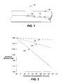
- Fig. 1 is a drawing showing a conventional optical fiber waveguide
- Fig. 2A is a drawing showing a first optical waveguide according to an embodiment of the present invention.
- Fig. 2B is a drawing showing a sectional view of the optical waveguide of Fig. 2A;
- Fig. 3 is a chart of the indexes of refraction of example polymers as a function of temperature
- Fig. 4A is a drawing showing a second optical waveguide according to another embodiment of the present invention.
- Fig. 4B is a drawing showing a sectional view of the second optical waveguide of Fig. 4A;
- Fig. 5 is a drawing showing an optical waveguide system that employs a thermo-electric heater with the optical waveguide of Fig. 2A according to another embodiment of the present invention.
- Fig. 6 is a drawing showing an optical waveguide system that employs a laser source with the optical waveguide of Fig. 2A according to yet another embodiment of the present invention.
- a waveguide which comprises a conventional optical fiber 50.
- the optical fiber 50 comprises a core 55 surrounded by a cladding 60.
- the core 55 is comprised of a material such as, for example, doped silica with an index of refraction of n1.
- the cladding 60 is comprised of a material such as, for example, silica with an index of refraction of n2.
- the optical fiber 50 operates as a waveguide for light radiation 65 when n1 is greater than n2 as is known by those skilled in the art. When n1 is less than or equal to n2, the light radiation 65 leaves the core and will not propagate along the core 55.
- the waveguide structure 100 includes a doped silica core 105 which is formed on a silica substrate 110.
- the doped silica core 105 is surrounded by a silica cladding material 115 which encloses the remaining sides of the core 105 not bounded by the silica substrate 110.
- a polymer cladding material 120 encloses the remaining sides of the core 105 instead of the silica cladding material 115.
- the doped silica core 105 has an index of refraction of n1
- the silica substrate 110 has an index of refraction of n2
- the silica cladding material 115 has an index of refraction of nC
- the polymer cladding material 120 has an index of refraction of nP.
- a dashed line 122 indicates a cutting plane through the waveguide structure 100 at the polymer cladding material 120.
- Fig. 2B shown is a sectional view 123 of the waveguide structure 100 taken along the dashed line 122 which further illustrates the core 105, substrate 110, and the polymer cladding material 120.
- the polymer cladding material 120 is taken from the general category of materials classified as polymers which generally are chemical compounds with high molecular weight comprising a number of structural units linked together by covalent bonds. Polymers which qualify for use as the polymer cladding material 120 should generally possess the optical characteristics including an index of refraction that varies with temperature as will be discussed.
- the core 105 comprises doped silica and the substrate 110 comprises silica
- other materials may be employed as known by those skilled in the art. Consequently, an exhaustive list of possible materials used to create these components is not offered herein.
- the waveguide structure 100 is for illustrative purposes and is not the only structural configuration possible. It may be possible for example, that the polymer cladding material 120 only contact the doped silica core 105 in specified regions such as on the upper surface of the doped silica core 105, for example.
- the design of the actual waveguide structure 100 is such that the polymer cladding material 120 comes into contact with the doped silica core 110 so that the propagation of light radiation through the core 110 can be manipulated by controlling the index of refraction of the polymer cladding material 120 relative to the index of refraction of the doped silica core 105 to achieve certain advantages.
- the polymer cladding material 120 features a relatively high hermo-optic coefficient ⁇ n p / ⁇ T due to the fact that the index of refraction of polymers can vary significantly with changing temperature.
- the thermo-optic coefficient ⁇ n p / ⁇ T generally may be as high as -.0001 C -1 and even up to-.0003 C -1 , where n P is the refractive index of the polymer and T is temperature.
- the thermo-optic coefficient of silica is much lower and of opposite polarity, being on the order of +.00001 C -1 . Consequently, the index of refraction of fused silica and other similar materials will not change significantly when subjected to heat, while the index of refraction of the polymer will change significantly.
- Fig. 3 shown is a graph depicting the index of refraction as a function of temperature in degrees Celsius of three example polymers which may be used according to the various embodiments of the present invention.
- Line 130 depicts the index of refraction of F/CA polymer which has a thermal coefficient of -.00002 C -1
- line 135 depicts the index of refraction of D-PMMA/D-FA polymer which has a thermal coefficient of -.0003 C -1
- line 140 depicts the index of refraction of FA polymer which has a thermal coefficient of -.0003 C -1 .
- the indexes of refraction of various polymers depend upon their composition and can vary over a relatively wide range as a function of temperature.
- the change of the index of refraction of a polymer cladding as contemplated herein provides distinct advantages.
- a change in the propagation constant b of the guided optical wave through the core can be made by changing the temperature of the polymer cladding.
- the propagation of light radiation through the core may be diminished or stopped by raising the index of refraction of the polymer cladding above that of the core.
- a second waveguide structure 150 according to another embodiment of the present invention.
- the waveguide structure 150 features a polymer core 155 formed on a substrate material 160 and surrounded on the remaining sides by a cladding material 165.
- the cladding material 165 may be another polymer or other material that has an index of refraction that allows the propagation of light through the polymer core 155.
- the relative indexes of refraction of the polymer core 155 and the cladding material 165 are manipulated to achieve the desired propagation through the waveguide structure 150.
- Fig. 4B shows is a sectional view of the waveguide structure 150.
- the waveguide system 200 features the waveguide structure 100 (Fig. 2A) which includes the polymer cladding material 120 with the doped silica core 105 formed on the silica substrate 110.
- the waveguide system 200 further includes a thermo-electric heater 205 and a thermo-electric cooler 210.
- the thermo-electric heater 205 is electrically coupled to a voltage source V1 and may be of the chrome strip type. Other types of thermo-electric heaters 205 may include electrically conducting glass materials.
- the thermo-electric cooler 210 is electrically coupled to a voltage source V 2 .
- the waveguide system 200 may be constructed with the thermo-electric heater 205 alone or with the thermo-electric cooler 210 alone depending on the ambient temperature and the desired range for the index of refraction of the polymer material.
- the waveguide system 200 is formed, for example, on an integrated optical circuit which are well known by those skilled in the art and not discussed here in detail.
- a second waveguide system 300 according to yet another embodiment of the present invention.
- the waveguide system 300 also features the waveguide structure 100 (Fig. 2B) which includes the polymer cladding material 120 with the doped silica core 105 formed on the silica substrate 110.
- the waveguide system 300 includes a laser source 305 which produces laser radiation 310.
- the laser source 305 is directed such that the laser radiation 310 falls onto the polymer cladding material 120.
- the laser radiation 310 heats up the polymer cladding material 120 resulting in a corresponding change in the index of refraction of the polymer cladding material 120.
- a thermo-electric cooler 210 (Fig. 5) may be included in the waveguide system 300 similar to the waveguide system 200.
Landscapes
- Physics & Mathematics (AREA)
- Nonlinear Science (AREA)
- General Physics & Mathematics (AREA)
- Optics & Photonics (AREA)
- Engineering & Computer Science (AREA)
- Microelectronics & Electronic Packaging (AREA)
- Optical Integrated Circuits (AREA)
- Optical Modulation, Optical Deflection, Nonlinear Optics, Optical Demodulation, Optical Logic Elements (AREA)
Applications Claiming Priority (2)
| Application Number | Priority Date | Filing Date | Title |
|---|---|---|---|
| US134121 | 1993-10-08 | ||
| US09/134,121 US6856734B1 (en) | 1998-08-14 | 1998-08-14 | Waveguide structure using polymer material and method |
Publications (1)
| Publication Number | Publication Date |
|---|---|
| EP0981064A1 true EP0981064A1 (de) | 2000-02-23 |
Family
ID=22461857
Family Applications (1)
| Application Number | Title | Priority Date | Filing Date |
|---|---|---|---|
| EP99306129A Withdrawn EP0981064A1 (de) | 1998-08-14 | 1999-08-02 | Wellenleiterstruktur unter Verwendung von polymerem Material und Verfahren |
Country Status (3)
| Country | Link |
|---|---|
| US (1) | US6856734B1 (de) |
| EP (1) | EP0981064A1 (de) |
| JP (1) | JP2000066044A (de) |
Cited By (5)
| Publication number | Priority date | Publication date | Assignee | Title |
|---|---|---|---|---|
| WO2000028355A3 (en) * | 1998-11-10 | 2000-10-05 | Lightwave Microsystems Corp | Photonic devices comprising thermo-optic polymer |
| WO2001067166A1 (en) * | 2000-03-03 | 2001-09-13 | Lightwave Microsystems Corporation | Variable optical attenuators |
| US6434318B1 (en) | 2000-08-02 | 2002-08-13 | Gemfire Corporation | Device and method for variable attenuation of an optical channel |
| US6507681B1 (en) | 2000-08-02 | 2003-01-14 | Gemfire Corporation | Anti-waveguide routing structure |
| US7127135B2 (en) | 2004-05-14 | 2006-10-24 | Sumitomo Electric Industries, Ltd. | Optical device with lightwave circuit element |
Families Citing this family (4)
| Publication number | Priority date | Publication date | Assignee | Title |
|---|---|---|---|---|
| KR100905658B1 (ko) * | 2007-07-04 | 2009-06-30 | 인하대학교 산학협력단 | 폴리머 크래드의 굴절률 조절에 의한 비선형 실리콘광도파로 소자 및 그 제조 방법 |
| WO2014023804A2 (en) * | 2012-08-08 | 2014-02-13 | Fraunhofer-Gesellschaft zur Förderung der angewandten Forschung e. V. | Directional coupler and optical waveguide |
| CN105829956A (zh) * | 2014-04-17 | 2016-08-03 | 华为技术有限公司 | 热光移相器 |
| US10197818B2 (en) * | 2016-10-24 | 2019-02-05 | Electronics & Telecommunications Research Institute | Thermo-optic optical switch |
Citations (4)
| Publication number | Priority date | Publication date | Assignee | Title |
|---|---|---|---|---|
| JPS5975228A (ja) * | 1982-10-22 | 1984-04-27 | Omron Tateisi Electronics Co | 光スイツチ |
| US4685766A (en) * | 1983-01-22 | 1987-08-11 | Canon Kabushiki Kaisha | Optical device |
| EP0444582A2 (de) * | 1990-02-26 | 1991-09-04 | Nippon Telegraph And Telephone Corporation | Optische Wellenleiterschaltung und Verfahren zum Justieren einer ihrer Charakteristiken |
| EP0642052A1 (de) * | 1993-08-24 | 1995-03-08 | Akzo Nobel N.V. | Optische Wellenleiteranordnung aus Polymermaterial mit thermooptischen Eigenschaften |
Family Cites Families (7)
| Publication number | Priority date | Publication date | Assignee | Title |
|---|---|---|---|---|
| GB8328204D0 (en) * | 1983-10-21 | 1983-11-23 | British Telecomm | Optical fibres |
| JPS60186808A (ja) * | 1984-03-06 | 1985-09-24 | Sumitomo Chem Co Ltd | 光伝送繊維 |
| JPH0646244B2 (ja) * | 1985-05-17 | 1994-06-15 | 三菱レイヨン株式会社 | プラスチック系光ファイバ |
| KR910000615B1 (ko) * | 1986-02-20 | 1991-01-28 | 더 다우 케미칼 캄파니 | 중합체 광섬유 |
| GB2196148B (en) * | 1986-09-09 | 1990-03-28 | Central Glass Co Ltd | Optical fiber using vinylidene fluoride base ternary copolymer as cladding material |
| US5292620A (en) * | 1988-01-15 | 1994-03-08 | E. I. Du Pont De Nemours And Company | Optical waveguide devices, elements for making the devices and methods of making the devices and elements |
| US4979796A (en) * | 1989-12-15 | 1990-12-25 | The Charles Stark Draper Laboratory, Inc. | Thermally controlled optical fiber |
-
1998
- 1998-08-14 US US09/134,121 patent/US6856734B1/en not_active Expired - Lifetime
-
1999
- 1999-08-02 EP EP99306129A patent/EP0981064A1/de not_active Withdrawn
- 1999-08-13 JP JP11228977A patent/JP2000066044A/ja active Pending
Patent Citations (4)
| Publication number | Priority date | Publication date | Assignee | Title |
|---|---|---|---|---|
| JPS5975228A (ja) * | 1982-10-22 | 1984-04-27 | Omron Tateisi Electronics Co | 光スイツチ |
| US4685766A (en) * | 1983-01-22 | 1987-08-11 | Canon Kabushiki Kaisha | Optical device |
| EP0444582A2 (de) * | 1990-02-26 | 1991-09-04 | Nippon Telegraph And Telephone Corporation | Optische Wellenleiterschaltung und Verfahren zum Justieren einer ihrer Charakteristiken |
| EP0642052A1 (de) * | 1993-08-24 | 1995-03-08 | Akzo Nobel N.V. | Optische Wellenleiteranordnung aus Polymermaterial mit thermooptischen Eigenschaften |
Non-Patent Citations (3)
| Title |
|---|
| DUGAS J ET AL: "BEHAVIOR OF THE REFRACTIVE INDEX AND OF THE COEFFICIENT OF THERMAL EXPANSION OF SILICONE WITH TEMPERATURE", APPLIED OPTICS,US,OPTICAL SOCIETY OF AMERICA,WASHINGTON, vol. 25, no. 21, pages 3907-3908, XP002023243, ISSN: 0003-6935 * |
| MOSHREFZADEH R S ET AL: "TEMPERATURE DEPENDENCE OF INDEX OF REFRACTION OF POLYMERIC WAVEGUIDES", JOURNAL OF LIGHTWAVE TECHNOLOGY,US,IEEE. NEW YORK, vol. 10, no. 4, pages 420-425, XP000272899, ISSN: 0733-8724 * |
| PATENT ABSTRACTS OF JAPAN vol. 008, no. 183 (P - 296) 23 August 1984 (1984-08-23) * |
Cited By (6)
| Publication number | Priority date | Publication date | Assignee | Title |
|---|---|---|---|---|
| WO2000028355A3 (en) * | 1998-11-10 | 2000-10-05 | Lightwave Microsystems Corp | Photonic devices comprising thermo-optic polymer |
| US6311004B1 (en) | 1998-11-10 | 2001-10-30 | Lightwave Microsystems | Photonic devices comprising thermo-optic polymer |
| WO2001067166A1 (en) * | 2000-03-03 | 2001-09-13 | Lightwave Microsystems Corporation | Variable optical attenuators |
| US6434318B1 (en) | 2000-08-02 | 2002-08-13 | Gemfire Corporation | Device and method for variable attenuation of an optical channel |
| US6507681B1 (en) | 2000-08-02 | 2003-01-14 | Gemfire Corporation | Anti-waveguide routing structure |
| US7127135B2 (en) | 2004-05-14 | 2006-10-24 | Sumitomo Electric Industries, Ltd. | Optical device with lightwave circuit element |
Also Published As
| Publication number | Publication date |
|---|---|
| JP2000066044A (ja) | 2000-03-03 |
| US6856734B1 (en) | 2005-02-15 |
Similar Documents
| Publication | Publication Date | Title |
|---|---|---|
| US6240226B1 (en) | Polymer material and method for optical switching and modulation | |
| US6310999B1 (en) | Directional coupler and method using polymer material | |
| US6208798B1 (en) | Variable optical attenuator with thermo-optic control | |
| Cao et al. | Additive manufacturing of highly reconfigurable plasmonic circuits for terahertz communications | |
| Noh et al. | Polymer waveguide variable optical attenuator and its reliability | |
| JP2004533390A (ja) | 高屈折率コントラストの光導波路および用途 | |
| US5438640A (en) | Optical waveguide device for receiving functional component | |
| US6385383B1 (en) | Optical attenuator structure and method using polymer material | |
| US6856734B1 (en) | Waveguide structure using polymer material and method | |
| WO2003100506A1 (en) | Method and apparatus for optical mode conversion | |
| US4737002A (en) | Tunable optical directional couplers | |
| CA2281451A1 (en) | Optical intensity modulator and switch comprising the same | |
| CA2311961A1 (en) | Slotted monolithic optical waveguides | |
| Garner et al. | Variable optical attenuator for large-scale integration | |
| JP3337629B2 (ja) | 導波路型光可変減衰器 | |
| Zembutsu et al. | Waveguiding properties of (Se, S)-based chalcogenide glass films and some applications to optical waveguide devices | |
| JPH10227930A (ja) | 温度無依存光導波路およびその製造方法 | |
| EP1177466A1 (de) | Faseroptisches dämpfungsglied und verfahren zur dämpfung von durch eine optische faser transmittiertem licht | |
| JPH11507741A (ja) | マッハ・ツェンダ・スイッチ | |
| Nishimura et al. | Control of spectral characteristics of dispersive optical fibers by annealing | |
| GB2329721A (en) | Optical attenuator | |
| EP1250627A2 (de) | Optische vorrichtung | |
| Sahu | Polarization independent thermally tunable erbium-doped fiber amplifier gain equalizer using a cascaded Mach–Zehnder coupler | |
| JP3800039B2 (ja) | 熱光学型光アテネータ | |
| JP3835205B2 (ja) | 熱光学効果型光アテネータ |
Legal Events
| Date | Code | Title | Description |
|---|---|---|---|
| PUAI | Public reference made under article 153(3) epc to a published international application that has entered the european phase |
Free format text: ORIGINAL CODE: 0009012 |
|
| AK | Designated contracting states |
Kind code of ref document: A1 Designated state(s): DE FR GB |
|
| AX | Request for extension of the european patent |
Free format text: AL;LT;LV;MK;RO;SI |
|
| 17P | Request for examination filed |
Effective date: 20000811 |
|
| AKX | Designation fees paid |
Free format text: DE FR GB |
|
| RAP1 | Party data changed (applicant data changed or rights of an application transferred) |
Owner name: AGERE SYSTEMS OPTOELECTRONICS GUARDIAN CORPORATION |
|
| RAP1 | Party data changed (applicant data changed or rights of an application transferred) |
Owner name: TRIQUINT TECHNOLOGY HOLDING CO |
|
| STAA | Information on the status of an ep patent application or granted ep patent |
Free format text: STATUS: THE APPLICATION IS DEEMED TO BE WITHDRAWN |
|
| 18D | Application deemed to be withdrawn |
Effective date: 20040302 |