EP0981153A2 - Vorrichtung und Verfahren zur Strahlungsheizung - Google Patents
Vorrichtung und Verfahren zur Strahlungsheizung Download PDFInfo
- Publication number
- EP0981153A2 EP0981153A2 EP99306344A EP99306344A EP0981153A2 EP 0981153 A2 EP0981153 A2 EP 0981153A2 EP 99306344 A EP99306344 A EP 99306344A EP 99306344 A EP99306344 A EP 99306344A EP 0981153 A2 EP0981153 A2 EP 0981153A2
- Authority
- EP
- European Patent Office
- Prior art keywords
- reflector
- temperature
- wafer
- radiant
- workpiece
- Prior art date
- Legal status (The legal status is an assumption and is not a legal conclusion. Google has not performed a legal analysis and makes no representation as to the accuracy of the status listed.)
- Withdrawn
Links
Images

Classifications
-
- H—ELECTRICITY
- H10—SEMICONDUCTOR DEVICES; ELECTRIC SOLID-STATE DEVICES NOT OTHERWISE PROVIDED FOR
- H10P—GENERIC PROCESSES OR APPARATUS FOR THE MANUFACTURE OR TREATMENT OF DEVICES COVERED BY CLASS H10
- H10P72/00—Handling or holding of wafers, substrates or devices during manufacture or treatment thereof
- H10P72/04—Apparatus for manufacture or treatment
- H10P72/0431—Apparatus for thermal treatment
- H10P72/0436—Apparatus for thermal treatment mainly by radiation
Definitions
- the present invention is directed to a radiant heating apparatus and method, for use with semiconductor manufacturing equipment.
- zone control One approach to attaining a uniform temperature is called "zone control".
- zone control a plurality of radiant heating units such as infrared lamps are divided into zones and the lamps in a given zone receive the same power, while lamps in different zones may receive different power, to result in uniform temperature across the wafer. While zone control is advantageous in some applications, it requires complex electronic controls of the power applied to the lamps.
- a high temperature, rapid thermal process using flood heating is known. With flood heating, a temperature inversion may be observed wherein the edge of the workpiece is hotter during the ramping phase, while the center of the wafer is hotter during the steady state phase. It has been recognized that this is undesirable in the high temperature environment (e.g. 1150°C) of rapid thermal processing because the edge to center temperature differences at such process temperature create stresses which can damage the workpiece.
- high temperature environment e.g. 1150°C
- the inventors have discovered that as applied to a low temperature process (wherein the wafer temperature is kept below about 400°C), the above-discussed temperature inversion effect is highly desirable because it tends to reduce the center to edge cumulative temperature gradient as the process is performed. Since in the first part of the process (ramping phase), the edge of the workpiece is hotter than the center, while in the second part (steady state phase) the center is hotter than the edge, the area under the center to edge temperature gradient curve (cumulative temperature gradient) is first negative and then positive, with the total area being smaller than if the gradient were only in one direction, resulting in a more uniform process. Furthermore, the temperature stresses created by such inversion within appropriate limits do not damage the wafer in a low temperature process. This uniform process is then achieved without using an expensive and complex system such as zone control.
- a radiant heating apparatus including a plurality of reflecting units, wherein each reflecting unit comprises a back reflector, a tubular reflector extending from said back reflector towards the workpiece region, and a radiant energy source disposed in said tubular reflector in front of the back reflector, wherein a cross section of the tubular reflector is in the shape of a truncated segment of a circle.
- reflecting units having a diffuse back reflector and a specular tubular reflector.
- a reflecting structure for retrofitting a pre-existing array of ellipsoidal reflectors is provided.
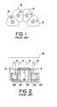
- Figures 1 and 2 show a prior art reflector array for use in radiant heating of a semiconductor workpiece.
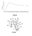
- Figure 3 is a graph of the center to edge temperature gradient using the reflector array of Figures 1 and 2 for a low temperature process.
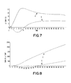
- Figure 4 is a perspective view of an embodiment of the invention.
- Figure 5 is a plan view of the embodiment shown in Figure 4.
- Figure 6 shows a side view of the embodiment shown in Figure 4 with a process chamber.
- Figure 7 is a graph of the comparison of the center to edge temperature gradient obtained with the apparatus of the invention and with the prior art reflector array.
- Figure 8 is a comparison of the cumulative center to edge temperature gradient obtained with the apparatus of the invention and with the prior art reflector array.
- Figures 1 and 2 depict a prior art radiant heating reflector array for use with semiconductor process chambers.
- Figure 1 which is a plan view, four ellipsoidal reflectors 2, 4, 6, and 8 are shown (half the entire 360° ring array), wherein the reflectors are associated with respective lamps 10, 12, 14, and 16.
- the lamps are infrared producing, such as quartz halogen type, and referring to Figure 2, which is a side view, the reflectors are seen concentrating heat energy on a semiconductor workpiece, wafer 18.
- a support structure for the reflectors is also shown comprised of base 20 and strut members 22, 24, 26, and 28.
- the reflecting units are positioned so as to irradiate a region near the edge of the wafer. This is because the center, by virtue of its geometric location, would get hotter than the edge if irradiation were uniform across the wafer.
- the temperature of the wafer may remain substantially uniform across its surface area during processing so as to promote the performance of a uniform process.
- the process may be any of the many processes performed on semiconductor wafers including but not limited to, ashing, etching, and residue removal.
- the invention is concerned with low temperature processes, i.e., those during which the wafer remains below about 400°C, and the graph in Figure 3 depicts the center to edge temperature gradient for a 270°C process.
- the process is divided into a temperature ramping phase and a temperature steady state phase.
- the power applied to the lamp filament is higher than in the steady state phase, so as to cause the wafer temperature to ramp up to the appropriate temperature.
- the power is reduced and the steady state phase ensues.
- the temperature is generally more non-uniform during the ramping phase than during the steady state phase.
- the ramping phase lasts about 25 seconds, and the maximum temperature gradient exceeds about 26°C.
- the temperature gradient is about 20°C.
- FIG. 4 an embodiment of the invention is depicted.
- a reflecting structure 30 is added to the prior art array shown in Figures 1 and 2.
- Reflecting structure 30 is configured so as to result in a temperature inversion effect at the wafer, that is during the ramping phase, the edge of the wafer is hotter than the center, while during the steady state phase, the reverse is true. Since the center to edge temperature gradient is first negative and then positive, the cumulative temperature gradient, indicative of how uniform the temperature is as a function of elapsed time is reduced, resulting in a more uniform process.
- reflector structure 30 is comprised of cylindrical band 32, radially extending partitions 34, and flat inner members 36. These are bonded together so as to form reflecting units, each of which is comprised of a back reflector (ellipsoidal members) and a tubular reflector which is comprised of a portion of cylindrical band 32, two adjacent partitions 34, and flat inner member 36.
- a cross-section of the tubular reflector is in the shape of a truncated segment of a circle.
- the inner surfaces of the tubular reflector are specular, as by being made of aluminum or Alzak and/or having a polished finish applied. On the other hand, the finish of the back reflector is diffuse. It should be appreciated that while only half of a ring of lamps is shown, for ease of illustration, in an actual embodiment a full ring would be used.
- the radiant heating apparatus is shown being used to heat semiconductor wafer 42, which is disposed on support structure 44 in process chamber 46.
- process chamber 46 is used for afterglow plasma ashing
- plasma species are fed in through the top, and mesh structure 50, 52 is effective to uniformly disperse it on wafer 42 to effect ashing, the waste products being drawn down by a vacuum applied to bottom opening 54.
- a vacuum line (not shown) may pass through the center opening in the reflector structure.
- a programmable power supply 58 feeds power to the lamps.
- Such apparatus is well known to those skilled in the art, and is comprised of a power supply which can be programmed to supply different power levels for selected periods of time. In the present case, the power supply is arranged so as to provide a relatively higher power during the ramping phase and a lower power during the steady state phase.
- the reflecting partitions 34 and the flat inner members 36 are close to the lamps, thus preventing heat from the lamps from being directed to the center of the wafer.
- the cross sectional area of the tubular reflectors is non-circular, so that the lengthwise multiple reflections result in more uniform radiation at the wafer. It is noted that the radiation is emitted mostly perpendicular to the long direction of the lamp filaments to the walls of the tubular reflector, where after multiple reflections it exits at the top of the tubular reflector. According to the laws of optics, the irregular (non-circular) cross sectional shape of the tubular reflectors results in more uniform radiation at the exit end.
- Figure 7 is a comparison of the center to edge temperature gradient obtained with the prior art arrangement and with the invention.
- curve A depicts the temperature gradient with the prior art arrangement using ellipsoidal reflectors.
- Curve B depicts the gradient utilizing the embodiment of the invention depicted in Figures 4 to 6. It is seen that a temperature inversion effect is produced, wherein the edge is hotter than the center during the ramping phase while the center is hotter than the edge during the steady state phase.
- curve B it is seen that with the invention, after fast ramping, the gradient slowly resumes the center to edge orientation, but due to the inversion, it keeps low absolute values.
- ashing and etching processes are, among other factors, proportional to the temperature. So, the difference of ashing/etching from center to edge is a function of the integral of the center to edge temperature gradient during the process time.
- Figure 8 shows the cumulative values of the temperature gradient for the prior art and the invention.
- integral always increases, causing the process to be always non-uniform.
- the process non-uniformity is minimized.
- one minute processes are optimized wherein the cumulative temperature gradient is zeroed.
- the reflecting structure of the invention causes the temperature inversion to take place is that the structure redirects the radiant energy from the center of the workpiece as in the prior art, to the edge.
- the dominant heating mechanism is the radiant energy from the lamps which causes the workpiece to be heated from the edge to the center, thus causing the former to be hotter than the latter.
- this edge to center heating is no longer the dominant heating mechanism. Instead, the heat conduction inside the workpiece, the wall effect, the contribution of the chamber and the ashing/etching process, all cause the gradient temperature to be outward.
- the ellipsoidal reflector array of the prior art is retrofitted with the reflecting structure 30.Such structure is merely set over the pre-existing array, with partitions 34 being press-fit in the spaces between adjacent reflectors, while bottoms of the partitions rest on the back reflectors. Inner members 36 are bent over at the top to provide reflecting plates 40, which may promote reflection efficiency. In other implementations of the invention, an entire structure may be provided as a new piece of equipment. In such implementations, the back reflectors need not be ellipsoidal.
Landscapes
- Drying Of Semiconductors (AREA)
- Control Of Resistance Heating (AREA)
Applications Claiming Priority (2)
| Application Number | Priority Date | Filing Date | Title |
|---|---|---|---|
| US09/134,865 US6023555A (en) | 1998-08-17 | 1998-08-17 | Radiant heating apparatus and method |
| US134865 | 1998-08-17 |
Publications (2)
| Publication Number | Publication Date |
|---|---|
| EP0981153A2 true EP0981153A2 (de) | 2000-02-23 |
| EP0981153A3 EP0981153A3 (de) | 2003-08-20 |
Family
ID=22465368
Family Applications (1)
| Application Number | Title | Priority Date | Filing Date |
|---|---|---|---|
| EP99306344A Withdrawn EP0981153A3 (de) | 1998-08-17 | 1999-08-11 | Vorrichtung und Verfahren zur Strahlungsheizung |
Country Status (3)
| Country | Link |
|---|---|
| US (1) | US6023555A (de) |
| EP (1) | EP0981153A3 (de) |
| JP (1) | JP4565365B2 (de) |
Cited By (1)
| Publication number | Priority date | Publication date | Assignee | Title |
|---|---|---|---|---|
| WO2004073050A1 (en) * | 2003-02-10 | 2004-08-26 | Axcelis Technologies Inc. | Radiant heating source |
Families Citing this family (4)
| Publication number | Priority date | Publication date | Assignee | Title |
|---|---|---|---|---|
| US6771895B2 (en) * | 1999-01-06 | 2004-08-03 | Mattson Technology, Inc. | Heating device for heating semiconductor wafers in thermal processing chambers |
| US6294394B1 (en) * | 1999-07-01 | 2001-09-25 | Voyan Technology | Ramp rate limiter to control stress during ramping |
| KR100807120B1 (ko) * | 2006-11-21 | 2008-02-27 | 코닉시스템 주식회사 | 급속열처리 장치 |
| JP5077198B2 (ja) | 2008-11-13 | 2012-11-21 | ウシオ電機株式会社 | 光照射装置 |
Family Cites Families (14)
| Publication number | Priority date | Publication date | Assignee | Title |
|---|---|---|---|---|
| US4640224A (en) * | 1985-08-05 | 1987-02-03 | Spectrum Cvd, Inc. | CVD heat source |
| US5158644A (en) * | 1986-12-19 | 1992-10-27 | Applied Materials, Inc. | Reactor chamber self-cleaning process |
| US4891499A (en) * | 1988-09-09 | 1990-01-02 | Texas Instruments Incorporated | Method and apparatus for real-time wafer temperature uniformity control and slip-free heating in lamp heated single-wafer rapid thermal processing systems |
| EP0511294B1 (de) * | 1990-01-19 | 1996-04-03 | Applied Materials, Inc. | Vorrichtung zum erwärmen von halbleiterscheiben oder -substraten |
| US5155336A (en) * | 1990-01-19 | 1992-10-13 | Applied Materials, Inc. | Rapid thermal heating apparatus and method |
| US5179677A (en) * | 1990-08-16 | 1993-01-12 | Applied Materials, Inc. | Apparatus and method for substrate heating utilizing various infrared means to achieve uniform intensity |
| US5436172A (en) * | 1991-05-20 | 1995-07-25 | Texas Instruments Incorporated | Real-time multi-zone semiconductor wafer temperature and process uniformity control system |
| CA2081055C (en) * | 1991-11-05 | 1999-12-21 | John R. Eppeland | Method and apparatus for heat treatment of metal parts utilizing infrared radiation |
| US5418885A (en) * | 1992-12-29 | 1995-05-23 | North Carolina State University | Three-zone rapid thermal processing system utilizing wafer edge heating means |
| US5504831A (en) * | 1993-11-10 | 1996-04-02 | Micron Semiconductor, Inc. | System for compensating against wafer edge heat loss in rapid thermal processing |
| US5561612A (en) * | 1994-05-18 | 1996-10-01 | Micron Technology, Inc. | Control and 3-dimensional simulation model of temperature variations in a rapid thermal processing machine |
| US5740314A (en) * | 1995-08-25 | 1998-04-14 | Edison Welding Institute | IR heating lamp array with reflectors modified by removal of segments thereof |
| JP3972379B2 (ja) * | 1995-12-14 | 2007-09-05 | 信越半導体株式会社 | 加熱炉 |
| DE69620590T2 (de) * | 1996-05-21 | 2002-11-21 | Applied Materials, Inc. | Verfahren und Vorrichtung zum Regeln der Temperatur einer Reaktorwand |
-
1998
- 1998-08-17 US US09/134,865 patent/US6023555A/en not_active Expired - Lifetime
-
1999
- 1999-08-11 EP EP99306344A patent/EP0981153A3/de not_active Withdrawn
- 1999-08-13 JP JP22915799A patent/JP4565365B2/ja not_active Expired - Fee Related
Cited By (2)
| Publication number | Priority date | Publication date | Assignee | Title |
|---|---|---|---|---|
| WO2004073050A1 (en) * | 2003-02-10 | 2004-08-26 | Axcelis Technologies Inc. | Radiant heating source |
| CN100401464C (zh) * | 2003-02-10 | 2008-07-09 | 艾克塞利斯技术公司 | 一种辐射加热源 |
Also Published As
| Publication number | Publication date |
|---|---|
| US6023555A (en) | 2000-02-08 |
| JP2000068223A (ja) | 2000-03-03 |
| JP4565365B2 (ja) | 2010-10-20 |
| EP0981153A3 (de) | 2003-08-20 |
Similar Documents
| Publication | Publication Date | Title |
|---|---|---|
| EP0119654B1 (de) | Ofen zur Wärmebehandlung von Halbleiterkörpern | |
| US6319556B1 (en) | Reflective surface for CVD reactor walls | |
| US5418885A (en) | Three-zone rapid thermal processing system utilizing wafer edge heating means | |
| JP3215155B2 (ja) | 照射による半導体ウェーハの急速熱処理方法 | |
| US4504323A (en) | Method for annealing semiconductors with a planar source composed of flash discharge lamps | |
| US6570134B2 (en) | Heat treatment device of the light irradiation type and heat treatment process of the irradiation type | |
| US4698486A (en) | Method of heating semiconductor wafers in order to achieve annealing, silicide formation, reflow of glass passivation layers, etc. | |
| EP0848575B1 (de) | Heizvorrichtung, Zusammenbau und Verfahren | |
| US4649261A (en) | Apparatus for heating semiconductor wafers in order to achieve annealing, silicide formation, reflow of glass passivation layers, etc. | |
| EP0811709B1 (de) | Verfahren und Vorrichtung zur Effizienzverbesserung strahlender Energiequellen für schnelle thermische Behandlung von Substraten durch Energiereflexion | |
| US4493977A (en) | Method for heating semiconductor wafers by a light-radiant heating furnace | |
| EP1593146B1 (de) | Strahlungs-wärme-quelle | |
| US6122440A (en) | Optical heating device for rapid thermal processing (RTP) system | |
| US6081072A (en) | Filament lamp for wafer heating and heating light source | |
| US4469529A (en) | Method for heating semiconductor wafer by means of application of radiated light with supplemental circumferential heating | |
| US6023555A (en) | Radiant heating apparatus and method | |
| US4468259A (en) | Uniform wafer heating by controlling light source and circumferential heating of wafer | |
| US5253324A (en) | Conical rapid thermal processing apparatus | |
| US7038173B2 (en) | Thermal processing apparatus and thermal processing method | |
| JP3789366B2 (ja) | 熱処理装置 | |
| JP3609380B2 (ja) | 熱処理装置 | |
| KR100807120B1 (ko) | 급속열처리 장치 | |
| JP2002506284A (ja) | 基板を熱処理するための装置 | |
| JP2000068223A5 (de) | ||
| JP2002075899A (ja) | 円形状平板試料の均熱装置 |
Legal Events
| Date | Code | Title | Description |
|---|---|---|---|
| PUAI | Public reference made under article 153(3) epc to a published international application that has entered the european phase |
Free format text: ORIGINAL CODE: 0009012 |
|
| AK | Designated contracting states |
Kind code of ref document: A2 Designated state(s): AT BE CH CY DE DK ES FI FR GB GR IE IT LI LU MC NL PT SE |
|
| AX | Request for extension of the european patent |
Free format text: AL;LT;LV;MK;RO;SI |
|
| RAP1 | Party data changed (applicant data changed or rights of an application transferred) |
Owner name: AXCELIS TECHNOLOGIES, INC. |
|
| PUAL | Search report despatched |
Free format text: ORIGINAL CODE: 0009013 |
|
| AK | Designated contracting states |
Designated state(s): AT BE CH CY DE DK ES FI FR GB GR IE IT LI LU MC NL PT SE |
|
| AX | Request for extension of the european patent |
Extension state: AL LT LV MK RO SI |
|
| 17P | Request for examination filed |
Effective date: 20031021 |
|
| AKX | Designation fees paid |
Designated state(s): DE FR GB IT NL |
|
| APBN | Date of receipt of notice of appeal recorded |
Free format text: ORIGINAL CODE: EPIDOSNNOA2E |
|
| RAP1 | Party data changed (applicant data changed or rights of an application transferred) |
Owner name: AXCELIS TECHNOLOGIES, INC. |
|
| APBR | Date of receipt of statement of grounds of appeal recorded |
Free format text: ORIGINAL CODE: EPIDOSNNOA3E |
|
| APAF | Appeal reference modified |
Free format text: ORIGINAL CODE: EPIDOSCREFNE |
|
| APBT | Appeal procedure closed |
Free format text: ORIGINAL CODE: EPIDOSNNOA9E |
|
| STAA | Information on the status of an ep patent application or granted ep patent |
Free format text: STATUS: THE APPLICATION IS DEEMED TO BE WITHDRAWN |
|
| 18D | Application deemed to be withdrawn |
Effective date: 20100302 |