EP0982576A1 - Sensor und verfahren zu dessen herstellung - Google Patents
Sensor und verfahren zu dessen herstellung Download PDFInfo
- Publication number
- EP0982576A1 EP0982576A1 EP99939217A EP99939217A EP0982576A1 EP 0982576 A1 EP0982576 A1 EP 0982576A1 EP 99939217 A EP99939217 A EP 99939217A EP 99939217 A EP99939217 A EP 99939217A EP 0982576 A1 EP0982576 A1 EP 0982576A1
- Authority
- EP
- European Patent Office
- Prior art keywords
- electrode
- electrode extraction
- solder
- cavity
- pad
- Prior art date
- Legal status (The legal status is an assumption and is not a legal conclusion. Google has not performed a legal analysis and makes no representation as to the accuracy of the status listed.)
- Granted
Links
Images




Classifications
-
- G—PHYSICS
- G01—MEASURING; TESTING
- G01L—MEASURING FORCE, STRESS, TORQUE, WORK, MECHANICAL POWER, MECHANICAL EFFICIENCY, OR FLUID PRESSURE
- G01L9/00—Measuring steady of quasi-steady pressure of fluid or fluent solid material by electric or magnetic pressure-sensitive elements; Transmitting or indicating the displacement of mechanical pressure-sensitive elements, used to measure the steady or quasi-steady pressure of a fluid or fluent solid material, by electric or magnetic means
- G01L9/12—Measuring steady of quasi-steady pressure of fluid or fluent solid material by electric or magnetic pressure-sensitive elements; Transmitting or indicating the displacement of mechanical pressure-sensitive elements, used to measure the steady or quasi-steady pressure of a fluid or fluent solid material, by electric or magnetic means by making use of variations in capacitance, i.e. electric circuits therefor
-
- G—PHYSICS
- G01—MEASURING; TESTING
- G01P—MEASURING LINEAR OR ANGULAR SPEED, ACCELERATION, DECELERATION, OR SHOCK; INDICATING PRESENCE, ABSENCE, OR DIRECTION, OF MOVEMENT
- G01P15/00—Measuring acceleration; Measuring deceleration; Measuring shock, i.e. sudden change of acceleration
- G01P15/02—Measuring acceleration; Measuring deceleration; Measuring shock, i.e. sudden change of acceleration by making use of inertia forces using solid seismic masses
- G01P15/08—Measuring acceleration; Measuring deceleration; Measuring shock, i.e. sudden change of acceleration by making use of inertia forces using solid seismic masses with conversion into electric or magnetic values
- G01P15/125—Measuring acceleration; Measuring deceleration; Measuring shock, i.e. sudden change of acceleration by making use of inertia forces using solid seismic masses with conversion into electric or magnetic values by capacitive pick-up
-
- G—PHYSICS
- G01—MEASURING; TESTING
- G01L—MEASURING FORCE, STRESS, TORQUE, WORK, MECHANICAL POWER, MECHANICAL EFFICIENCY, OR FLUID PRESSURE
- G01L9/00—Measuring steady of quasi-steady pressure of fluid or fluent solid material by electric or magnetic pressure-sensitive elements; Transmitting or indicating the displacement of mechanical pressure-sensitive elements, used to measure the steady or quasi-steady pressure of a fluid or fluent solid material, by electric or magnetic means
- G01L9/0041—Transmitting or indicating the displacement of flexible diaphragms
- G01L9/0072—Transmitting or indicating the displacement of flexible diaphragms using variations in capacitance
- G01L9/0075—Transmitting or indicating the displacement of flexible diaphragms using variations in capacitance using a ceramic diaphragm, e.g. alumina, fused quartz, glass
-
- G—PHYSICS
- G01—MEASURING; TESTING
- G01P—MEASURING LINEAR OR ANGULAR SPEED, ACCELERATION, DECELERATION, OR SHOCK; INDICATING PRESENCE, ABSENCE, OR DIRECTION, OF MOVEMENT
- G01P1/00—Details of instruments
- G01P1/02—Housings
- G01P1/023—Housings for acceleration measuring devices
-
- G—PHYSICS
- G01—MEASURING; TESTING
- G01P—MEASURING LINEAR OR ANGULAR SPEED, ACCELERATION, DECELERATION, OR SHOCK; INDICATING PRESENCE, ABSENCE, OR DIRECTION, OF MOVEMENT
- G01P15/00—Measuring acceleration; Measuring deceleration; Measuring shock, i.e. sudden change of acceleration
- G01P15/02—Measuring acceleration; Measuring deceleration; Measuring shock, i.e. sudden change of acceleration by making use of inertia forces using solid seismic masses
- G01P15/08—Measuring acceleration; Measuring deceleration; Measuring shock, i.e. sudden change of acceleration by making use of inertia forces using solid seismic masses with conversion into electric or magnetic values
- G01P15/0802—Details
-
- H—ELECTRICITY
- H10—SEMICONDUCTOR DEVICES; ELECTRIC SOLID-STATE DEVICES NOT OTHERWISE PROVIDED FOR
- H10W—GENERIC PACKAGES, INTERCONNECTIONS, CONNECTORS OR OTHER CONSTRUCTIONAL DETAILS OF DEVICES COVERED BY CLASS H10
- H10W20/00—Interconnections in chips, wafers or substrates
- H10W20/01—Manufacture or treatment
- H10W20/031—Manufacture or treatment of conductive parts of the interconnections
- H10W20/069—Manufacture or treatment of conductive parts of the interconnections by forming self-aligned vias or self-aligned contact plugs
-
- H—ELECTRICITY
- H10—SEMICONDUCTOR DEVICES; ELECTRIC SOLID-STATE DEVICES NOT OTHERWISE PROVIDED FOR
- H10W—GENERIC PACKAGES, INTERCONNECTIONS, CONNECTORS OR OTHER CONSTRUCTIONAL DETAILS OF DEVICES COVERED BY CLASS H10
- H10W70/00—Package substrates; Interposers; Redistribution layers [RDL]
- H10W70/60—Insulating or insulated package substrates; Interposers; Redistribution layers
- H10W70/62—Insulating or insulated package substrates; Interposers; Redistribution layers characterised by their interconnections
- H10W70/65—Shapes or dispositions of interconnections
- H10W70/654—Top-view layouts
- H10W70/655—Fan-out layouts
-
- H—ELECTRICITY
- H10—SEMICONDUCTOR DEVICES; ELECTRIC SOLID-STATE DEVICES NOT OTHERWISE PROVIDED FOR
- H10W—GENERIC PACKAGES, INTERCONNECTIONS, CONNECTORS OR OTHER CONSTRUCTIONAL DETAILS OF DEVICES COVERED BY CLASS H10
- H10W72/00—Interconnections or connectors in packages
- H10W72/90—Bond pads, in general
-
- H—ELECTRICITY
- H10—SEMICONDUCTOR DEVICES; ELECTRIC SOLID-STATE DEVICES NOT OTHERWISE PROVIDED FOR
- H10W—GENERIC PACKAGES, INTERCONNECTIONS, CONNECTORS OR OTHER CONSTRUCTIONAL DETAILS OF DEVICES COVERED BY CLASS H10
- H10W72/00—Interconnections or connectors in packages
- H10W72/90—Bond pads, in general
- H10W72/921—Structures or relative sizes of bond pads
- H10W72/923—Bond pads having multiple stacked layers
-
- H—ELECTRICITY
- H10—SEMICONDUCTOR DEVICES; ELECTRIC SOLID-STATE DEVICES NOT OTHERWISE PROVIDED FOR
- H10W—GENERIC PACKAGES, INTERCONNECTIONS, CONNECTORS OR OTHER CONSTRUCTIONAL DETAILS OF DEVICES COVERED BY CLASS H10
- H10W72/00—Interconnections or connectors in packages
- H10W72/90—Bond pads, in general
- H10W72/941—Dispositions of bond pads
- H10W72/9415—Dispositions of bond pads relative to the surface, e.g. recessed, protruding
-
- H—ELECTRICITY
- H10—SEMICONDUCTOR DEVICES; ELECTRIC SOLID-STATE DEVICES NOT OTHERWISE PROVIDED FOR
- H10W—GENERIC PACKAGES, INTERCONNECTIONS, CONNECTORS OR OTHER CONSTRUCTIONAL DETAILS OF DEVICES COVERED BY CLASS H10
- H10W90/00—Package configurations
- H10W90/701—Package configurations characterised by the relative positions of pads or connectors relative to package parts
- H10W90/721—Package configurations characterised by the relative positions of pads or connectors relative to package parts of bump connectors
- H10W90/724—Package configurations characterised by the relative positions of pads or connectors relative to package parts of bump connectors between a chip and a stacked insulating package substrate, interposer or RDL
Definitions
- the present invention relates to a sensor such as an electrostatic capacitance type pressure sensor for detecting the pressure of a medium to be measured or an acceleration sensor for measuring an acceleration, and a method of manufacturing the same and, more particularly, to an improvement of electrode extraction structures arranged to face each other.
- a plate-like stationary electrode and movable electrode are arranged parallel and close to each other so as to face each other within the cavity of a sensor main body.
- a change in capacitance between the two electrodes along with displacement of a diaphragm is detected to measure the pressure of a medium to be measured.
- Various pressure sensors have conventionally been proposed, as disclosed in Japanese Patent Laid-Open No. 6-265428 (to be referred to as a prior art).
- the electrode extraction structure in such pressure sensor is generally constituted by bonding a connection pin inserted through a cavity from an electrode extraction hole to an electrode with a bonding agent such as solder or paste (prepared by kneading a metal powder with a binder).
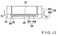
- Fig. 12 is a sectional view showing an electrostatic capacitance type pressure sensor described in the prior art.
- Fig. 13 is a sectional view taken along the line D - D' in Fig. 12.
- Fig. 14 is a sectional view taken along the line E - E' in Fig. 12.
- a sensor main body 202 is formed by first and second sapphire substrates 202A and 202B directly bonded to each other.
- a stationary electrode 201 and movable electrode 203 are arranged parallel to face each other in the sensor main body 202. This structure constitutes the electrostatic capacitance type sensor.
- the first substrate 202A is thicker than the second substrate 202B.
- Three electrode extraction holes 204 and one atmospheric pressure inlet hole 205 are formed through the first substrate 202A in the direction of thickness. These holes 204 and 205 allow a cavity 207 formed in the sensor main body 202 to communicate with the outside.
- a recess 208 is formed at the center of the inner surface of the second substrate 202B that faces the first substrate 202A.
- a space defined by the recess 208 and the inner surface of the first substrate 202A forms the cavity 207.
- the central portion of the second substrate 202B is made thin by the recess 208 to form a diaphragm 209.
- the second substrate 202B is directly bonded to the first substrate 202A through a thick outer peripheral portion 10.
- the first and second substrates 202A and 202B are made of the same material, do not sandwich any interposition on their bonded surface, and thus are almost free from any residual stress of bonding.
- the first and second substrates 202A and 202B can be used without causing any change over time which deforms the diaphragm 209, and can provide stable sensor characteristics.
- the movable electrode 203 is made up of a sensing electrode 203A having pressure sensitivity, and reference electrode 203B having almost no pressure sensitivity.
- the output difference between the two electrodes 203A and 202B can be detected to cancel the influence of temperature change and environmental change.
- the three electrode extraction holes 204 formed in the first substrate 202A correspond to the stationary electrode 201, sensing electrode 203A, and reference electrode 203B, respectively.
- the electrode extraction hole 204a is formed at a position where the hole 204a extends through an electrode extraction portion 214 formed on the stationary electrode 201.
- the electrode extraction holes 204b and 204c are respectively formed at positions corresponding to electrode extraction portions 215A and 215B formed on the sensing electrode 203A and reference electrode 203B.
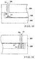
- FIG. 15 is an enlarged sectional view taken along the line F - F' in Fig. 13.
- Fig. 16 is an enlarged sectional view taken along the line G - G' in Fig. 13.
- connection pins 211 each having a lower end coated with a solder portion (or conductive paste) 212 are sequentially inserted (in practice, press-inserted) into the electrode extraction holes 204b and 204c for the movable electrode 203, and brought into contact with the electrode extraction portions 215A and 215B of the sensing electrode 203A and reference electrode 203B, respectively.
- the structure is heated in this state to temporarily fuse the solder portions 212, and then the solder portions 212 are cooled and solidify. This electrically connects the sensing electrode 203A and reference electrode 203B to the connection pins 211, as shown in Fig. 15.
- connection pin 211 having a lower end coated with a conductive paste 213 (or solder portion) is press-inserted into the electrode extraction hole 204a for the stationary electrode 201.
- the stationary electrode 201 and connection pin 211 are electrically connected through the conductive paste 213.
- the electrode 201 or 203 is mechanically, electrically connected to the connection pin 211 using the solder portion 212 or conductive paste 213. This poses the following problems.
- the solder portion 212 flows from the electrode extraction portion 215A or 215B to short-circuit the stationary electrode 201 and movable electrode 203.
- the conductive paste 213 When the conductive paste 213 is used as a bonding agent, a decrease in bonding strength and connection errors occur in an excessively small amount of conductive paste 213, similar to the solder portion 212. In an excessively large amount of conductive paste 213, the conductive paste 213 contacts the stationary electrode 201 to short-circuit the stationary electrode 201 and movable electrode 203.
- the stationary electrode 201 when the stationary electrode 201 is connected to the connection pin 211, the stationary electrode 201 is not formed on the abutment surface of the connection pin 211, as shown in Fig. 16. In other words, the stationary electrode 201 is formed on the inner surface of the sensor main body 202 in which the electrode extraction hole 204a is formed. For this reason, the solder portion is difficult to electrically connect the stationary electrode 201.
- the stationary electrode 201 may be somehow electrically connected using the conductive paste 213. However, similar to the movable electrode 203, the stationary electrode 201 may short-circuit with the movable electrode 203 or fail in connection depending on the amount of conductive paste 213.
- the present invention has been made to overcome the conventional drawbacks, and has as its object to realize a sensor having a high bonding strength between an electrode and a connection member such as a connection pin.
- a sensor according to the present invention is characterized by comprising a sensor main body (2) in which a cavity (7) which communicates with the outside through a plurality of electrode extraction holes (4a, 4b, 4c, 31, 104a, 104b, 104c, 131) is formed, a pair of electrodes (1, 3) arranged in the cavity to face each other, a plurality of connection members (11, 12, 111) which are inserted in the cavity through the electrode extraction holes and are electrically connected to corresponding electrodes, and pads (24, 25) which are formed in the cavity at positions where the pads face the electrode extraction holes, are bonded to corresponding connection members, and are made of a conductive material, wherein the wettability of each connection member for a pad surface is higher that the wettability of the connection member for an electrode surface.
- connection member Since the connection member has high wettability for the pad surface, part of the fused connection member spreads on the entire pad surface to firmly bond the connection member to the pad. As a result, the connection member can be reliably electrically connected to the electrode. To the contrary, the connection member has low wettability for the electrode surface. Even if part of the fused connection member overflows from the pad, it hardly flows along the electrode surface. For this reason, the connection member does not contact both a pair of electrodes, and does not short-circuit them.
- the pad (24) is formed on a surface of the electrode (3, 3A, 3B, 15A, 15B) present at a position where the electrode faces the electrode extraction hole (4a, 4b, 4c, 31), and the electrode is connected to a corresponding connection member (11, 12) through the pad.
- the electrode can be extracted through the connection member in a direction different from the electrode direction.
- connection member comprises a connection pin (11) inserted through the cavity from the electrode extraction hole, and a bonding agent (12) for bonding the connection pin to the pad. Since the connection member is formed by bonding the connection pin to the pad with the bonding agent, the connection member can be reliably electrically connected to the electrode.
- the senor When the bonding agent is made of Sn-Ag, the sensor may be constituted using Pt as the material of the electrode surface and Au as the material of the pad surface. This is because the wettability of Sn-Ag is high for Au and low for Pt.
- the pad (25) is formed at a position where the pad faces the electrode extraction hole, on a surface (21b) opposite to the electrode extraction hole side among inner surfaces (21a, 21b) of the sensor main body forming the cavity, and the electrode (1) formed on the electrode extraction hole side contacts a corresponding connection member (11, 12).
- the electrode can be extracted through the connection member in the same direction as the electrode direction.
- connection member comprises a connection pin (11) inserted into the cavity from the electrode extraction hole, and a bonding agent (12) for bonding the connection pin to the pad and the electrode formed on the electrode extraction hole side. Since the pad having high in wettability for the bonding agent is arranged at an opposite position, the bonding agent can reach the electrode surface through the connection pin to reliably electrically connect the electrode and connection pin. This reduces connection errors.
- the senor When the bonding agent is made of Sn-Ag, the sensor may be constituted using Pt as the material of the electrode surface and Au as the material of the pad surface.
- connection member in the sensor is made of solder for filling a space above the pad in the cavity and the electrode extraction hole (104a, 104b, 104c, 131) . Since the electrode extraction hole is filled with the solder which is used as the connection member, the connection member can be easily formed.
- the senor When the solder is made of Sn-Ag, the sensor may be constituted using Pt as the material of the electrode surface and Au as the material of the pad surface.
- the electrode extraction hole may be tapered to decrease the inner diameter from the outer surface to the inner surface of the sensor main body. This tapered shape can smoothly flow the fused solder.
- At least part of the inner surface of the electrode extraction hole may be covered with a material having high wettability for the solder. This can easily flow the fused solder through the electrode extraction hole.
- a sensor manufacturing method is characterized by comprising the steps of preparing a member in which a cavity (7) communicating with outside through a plurality of electrode extraction holes (104a, 104b, 104c, 131) is formed in a sensor main body (2), a pair of electrodes (1, 3) are arranged in the cavity to face each other, and a plurality of pads (24, 25) made of a conductive material higher in wettability for solder (111) than for the electrode are formed in the cavity at positions where the pads face the electrode extraction holes, flowing the fused solder from the electrode extraction holes onto the pads in the cavity to fill a space above the pads in the cavity and the electrode extraction holes with the fused solder, and cooling the fused solder to extract the electrodes in the cavity through the solder filled in the electrode extraction holes.
- This can form a sensor using the solder filling the electrode extraction hole as a connection member.
- the sensor manufacturing method may further comprise disposing a solder lump (111A) having a predetermined size at the inlet of each electrode extraction hole on the outer surface of the sensor main body, heating and fusing the solder lump, and flowing the solder lump from the electrode extraction hole.
- a solder lump (111A) having a predetermined size at the inlet of each electrode extraction hole on the outer surface of the sensor main body, heating and fusing the solder lump, and flowing the solder lump from the electrode extraction hole.
- the sensor manufacturing method further comprises attaching a jig (127) around the inlet of the electrode extraction hole, and disposing the solder lump.
- the solder lump can be disposed reliably at a desired position.
- the sensor manufacturing method further comprises increasing the external pressure of the sensor main body to be higher than the internal pressure of the cavity, and heating and fusing the solder.
- the fused solder can be forcibly flowed onto the pad.
- the solder is bonded to the pad.
- the electrode on an opposite side to the electrode extraction hole side can be extracted through the connection member made of the solder.
- the pad (25) is formed at a position where the pad faces the electrode extraction hole, on a surface (21b) opposite to the electrode extraction hole side among inner surfaces (21a, 21b) of the sensor main body forming the cavity, the solder is brought into contact with the electrode (1) formed on the electrode extraction hole side. Hence, the electrode on the electrode extraction hole side can be extracted through the connection member made of the solder.
- the electrode extraction hole can be formed using laser machining to taper the electrode extraction hole.
- Fig. 1 is a sectional view showing a sensor according to the first embodiment of the present invention.
- Fig. 2 is a sectional view taken along the line II - II' in Fig. 1.
- Fig. 3 is a sectional view taken along the line III - III' in Fig. 1.
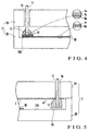
- Fig. 4 is an enlarged sectional view taken along the line IV - IV' in Fig. 2.
- Fig. 5 is an enlarged sectional view taken along the line V - V' in Fig. 2.
- Fig. 1 shows an electrostatic capacitance type pressure sensor to which the present invention is applied.
- a pressure sensor 20 comprises a sensor main body 2 formed by directly bonding first and second substrates 2A and 2B made of sapphire, silicon, glass, alumina, or the like.
- a cavity 7 is formed in the sensor main body 2.
- Three electrode extraction holes 4 (4a, 4b, 4c) communicating with the cavity 7, and one atmospheric pressure inlet hole 5 extend through the first substrate 2A.
- the cavity 7 is formed by a space defined by the first substrate 2A and a recess 8 formed at the center of the inner surface of the second substrate 2B.
- the central portion of the second substrate 2B is made thin by the recess 8 to form a diaphragm 9.
- a pair of stationary electrode 1 and movable electrode 3 (3A and 3B) are respectively formed on inner surfaces 21a and 21b close to each other that face each other through the cavity 7 between the first and second substrates 2A and 2B.
- the stationary electrode 1 and movable electrode 3 are made of Pt/bonding strengthening films.
- the bonding strengthening film is made of Ti, V, Cr, Nb, Zr, Hf, Ta, or the like.
- the stationary electrode 1 and movable electrode 3 are made of Pt/Nb. In this case, as shown in Fig. 4, each of the stationary electrode 1 and movable electrode 3 has a Pt upper layer and Nb lower layer.
- the movable electrode 3 is made up of the sensing electrode 3A having pressure sensitivity, and reference electrode 3B having almost no pressure sensitivity.
- Movable electrode extraction pads 24 made of a conductive material are formed on electrode extraction portions 15A and 15B of the sensing electrode 3A and reference electrode 3B.
- Each pad 24 is made of an Au/barrier layer/bonding strengthening film.
- the barrier layer is made of Pt, Ni, or the like.
- the bonding strengthening film is made of Ti, V, Cr, Nb, Zr, Hf, Ta, or the like, similar to the bonding strengthening film of the electrode.
- the pad 24 is made of Au/Pt/Nb. In this case, as shown in Fig. 4, the pad 24 has an Au upper layer, Pt middle layer, and Nb lower layer.
- the pads 24 are respectively connected to connection members for extracting the movable electrode 3 outside the sensor main body 2.
- the connection members are constituted by bonding connection pins 11 inserted through the electrode extraction holes 4b and 4c to the pads 24 with a bonding agent.
- a bonding agent a solder portion 12 or conductive paste is used.
- the solder portion 12 is made of Sn-Ag.
- the fused Sn-Ag solder portion 12 has very high wettability for Au forming the surface of the pad 24, and low wettability for Pt forming the surfaces of the stationary electrode 1 and movable electrode 3.
- connection pins 11 each having a lower end coated with the Sn-Ag solder portion 12 are press-inserted into the electrode extraction holes 4b and 4c to bring the Sn-Ag solder portions 12 into contact with the pads 24.
- the structure is heated to a predetermined temperature in this state to fuse the Sn-Ag solder portions 12.
- the Sn-Ag solder portions 12 are cooled to fix the connection pins 11 to the pads 24.
- the sensing electrode 3A and reference electrode 3B are electrically connected to the connection pins 11 through the pads 24 and Sn-Ag solder portions 12.
- the pads 24 each having an Au surface are formed on the electrode extraction portions 15A and 15B.
- the connection pins 11 are mechanically, electrically connected to the pads 24 through the Sn-Ag solder portions 12. Since the fused Sn-Ag solder portions 12 have very high wettability for the pads 24, the connection pins 11 can be connected with a satisfactory bonding strength. To the contrary, the Sn-Ag solder portions 12 have low wettability for the electrode material having a Pt surface. In other words, the Sn-Ag solder portions 12 hardly flow along the surfaces of the electrode extraction portions 15A and 15B. Hence, the Sn-Ag solder portions 12 do not contact the stationary electrode 1, and hardly short-circuit the stationary electrode 1 and movable electrode 3.
- a stationary electrode extraction conductive pad 25 is formed on the inner surface 21b of the second substrate 2B at a portion corresponding to an electrode extraction portion 14 of the first electrode 1.
- This pad 25 is made of the same material as the movable electrode pad 24.
- the pad 25 is connected to a stationary electrode connection pin 11 via an Sn-Ag solder portion (or conductive paste) 12 to form a connection member.
- the Sn-Ag solder portion 12 is brought into contact with the electrode extraction portion 14 of the stationary electrode 1 to electrically connect the stationary electrode 1 to the connection pin 11, thereby completing the electrostatic capacitance type pressure sensor.
- the stationary electrode 1 and connection pin 11 are connected using the Sn-Ag solder portion 12 and Au/Pt/Nb pad 25. Since the fused Sn-Ag solder portion 12 has high wettability for the pad 25, the connection pin 11 can be connected with satisfactory bonding strength.
- the Sn-Ag solder portion 12 spreads on the entire surface of the pad 25. In the pressure sensor 20 having the cavity 7 with a depth d of several ⁇ m, the Sn-Ag solder portion 12 spreads on the pad 25 so as to fill the cavity 7 by a capillary force, and comes into contact with the electrode extraction portion 14 of the stationary electrode 1. This can reliably electrically connect the stationary electrode 1 and connection pin 11. Since the Sn-Ag solder portion 12 has low wettability for the electrode material, the Sn-Ag solder member 12 does not contact the movable electrode 3, and does not short-circuit the stationary electrode 1 and movable electrode 3.
- connection pin 11 having a lower end coated with the Sn-Ag solder portion 12 is press-inserted into the electrode extraction hole 4.
- the present invention is not limited to this, and may employ a method of inserting a solder ball or solder column into a desired electrode extraction hole when the second substrate 2B is in a wafer state before dicing, then inserting a connection pin, and heating the structure. This method can also attain the same effects as those of the above-described method, and will enable to manufacture an electrostatic capacitance type pressure sensor having many electrode extraction structures formed at once.
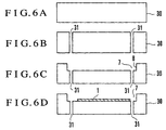
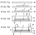
- FIGs. 6 and 7 respectively show sectional views of main steps in manufacturing the pressure sensor. Note that Figs. 6 and 7 show steps in manufacturing a pressure sensor in which a cavity, electrode extraction hole, and stationary electrode are formed on one substrate, and the other substrate is used as a diaphragm.
- a thick sapphire wafer 30 is prepared (Fig. 6(a)). Electrode extraction holes 31 and atmospheric pressure inlet hole (not shown) are formed through the sapphire wafer 30 (Fig. 6(b)). These electrode extraction holes 31 and an atmospheric pressure inlet hole are formed by machining, laser machining, ultrasonic machining, or the like.
- a recess 8 serving as a cavity 7 is formed to a desired depth in the inner surface of the sapphire wafer 30 (Fig. 6(c)).
- the recess 8 is formed by dry etching for a sapphire substrate material and by dry etching or wet etching for a glass or alumina substrate material.
- the planar shape of the cavity 7 may be circular, as shown in Fig. 2, or rectangular.
- a stationary electrode 1 is formed at a desired position on the bottom surface of the recess 8 (Fig. 6(d)).
- the stationary electrode 1 is made of a Pt/bonding strengthening film.
- the bonding strengthening film is made of Ti, V, Cr, Nb, Zr, Hf, Ta, or the like.
- the bonding strengthening film is formed by vacuum evaporation, ion plating, sputtering, or the like. To form the bonding strengthening film into an electrode shape, the film is formed using a shadow mask or photolithography and etching.
- a diaphragm wafer 35 is prepared (Fig. 7(a)).
- a movable electrode 3 is formed at a desired position on the inner surface of the diaphragm wafer 35 using the same material and method as those of the stationary electrode 1 (Fig. 7(b)).
- electrode extraction pads 24 and 25 are formed (Fig. 7(c)).
- Each pad is made of an Au/barrier layer/bonding strengthening film such as an Au/Pt/Nb film.
- the pads 24 and 25 are formed by vacuum evaporation, ion plating, sputtering, or the like.
- the substrates 30 and 35 are cleaned, and then directly bonded to each other at 400°C to 1,300°C to obtain a high bonding strength (Fig. 7(d)).
- connection pins 11 each having a lower end coated with an Sn-Ag solder portion 12 are press-inserted into the electrode extraction holes 31, heated and fused at 240°C to 300°C, and cooled to fix the connection pins 11 to the pads 24 and 25 (Fig. 7(e)).
- the stationary electrode 1, connection pin 11, and pad 25, and the movable electrode 3, pad 24, and connection pin 11 are mechanically, electrically bonded.
- the step of bonding the connection pin 11 is done after the wafer is divided into chips by dicing.
- the Sn-Ag solder portions 12 may be inserted and brought into contact with the electrodes before dicing in order to extract them at once.
- columnar Sn-Ag solder preforms are inserted into the electrode extraction holes 31, and heated at 240°C to 300°C to extract electrodes in a wafer state. This realizes mass production depending on the packaging method.
- Fig. 8 is a sectional view showing a sensor according to the second embodiment of the present invention.
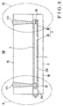
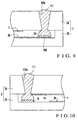
- Fig. 9 is an enlarged sectional view showing the portion IX in Fig. 8.
- Fig. 10 is an enlarged sectional view showing the portion A in Fig. 8. Similar to Fig. 1, Fig. 8 also shows an electrostatic capacitance type pressure sensor to which the present invention is applied. Note that the same reference numerals as in Figs. 1 to 5 denote same parts, and description thereof will be omitted.
- a pressure sensor 120 shown in Fig. 8 is different from the pressure sensor 20 shown in Fig. 1 in the structure of a connection member for extracting a stationary electrode 1 and movable electrode 3 in a cavity 7 outside a sensor main body 2. That is, electrode extraction holes 104a to 104c for communicating the cavity 7 with the outside are filled with solder portions 111 which are used as connection members.
- Movable electrode extraction pads 24 are respectively formed on electrode extraction portions 15A and 15B of a sensing electrode 3A and reference electrode 3B. Each pad 24 is identical to that shown in Fig. 4, and made of, e.g., Au/Pt/Nb.
- the solder portion 111 also functioning as a bonding agent is made of the same material Sn-Ag as the solder portion 12.
- Connection members for the movable electrode 3 are formed by flowing fused solder portions 111 in a sufficient amount into the electrode extraction holes 104b and 104c, and cooling the solder portions 111. At this time, since the fused solder portions 111 have very high wettability for the pads 24 having an Au surface, the solidified solder portions 111 are firmly bonded to the pads 24. On the other hand, the fused Sn-Ag solder portions 111 have low wettability for the electrode material having a Pt surface. Even if the flowed Sn-Ag solder portions 111 overflow from the pads 24, they hardly flow along the surfaces of the electrode extraction portions 15A and 15B, and do not short-circuit the stationary electrode 1 and movable electrode 3.
- a stationary electrode extraction conductive pad 25 is formed at a portion corresponding to an electrode extraction portion 14 of the first electrode 1 on an inner surface 21b of a second substrate 2B.
- This pad 25 is made of the same material as the movable electrode pad 24.
- a connection member for the stationary electrode 1 is formed similarly to the connection member for the movable electrode 3.
- the connection member and stationary electrode 1 are firmly bonded using the Sn-Ag solder portion 111 and pad 25 having an Au surface. Since the cavity 7 has the depth d of several ⁇ m, the Sn-Ag solder portion 111 spreads on the pad 25 so as to fill the cavity 7 by a capillary force, and comes into contact with the electrode extraction portion 14 of the stationary electrode 1. This can reliably electrically connect the stationary electrode 1 and the connection member made of the solder portion 111. Since the solder portion 111 has low wettability for the electrode material, the solder portion 111 does not short-circuit the stationary electrode 1 and movable electrode 3.
- the electrode extraction holes 104a to 104c are tapered to decrease their inner diameters from the outer surface to inner surface of the first substrate 2A.
- the tapered shape can smoothly flow the fused solder portions 111. Note that even if the electrode extraction holes 111 are not tapered, the fused solder portions 111 can be flowed. Thus, the electrode extraction holes need not always be tapered.
- Fig. 11 shows sectional views of main steps in manufacturing the pressure sensor. Note that Fig. 11 shows steps in manufacturing a pressure sensor in which a cavity, electrode extraction hole, and stationary electrode are formed on one substrate, and the other substrate is used as a diaphragm.
- a member shown in Fig. 11(a) is prepared. This member is formed by the same method as shown in Figs. 6(a) to 6(d) and Fig. 7(a) to 7(d).
- the inner diameter of each electrode extraction hole 131 is about 50 to 500 ⁇ m, and the height from the pad 24 or 25 to the outlet (a portion on the inner surface of a first substrate 130 forming the cavity 7) of the electrode extraction hole 131 is about 300 to 700 ⁇ m.
- the electrode extraction hole 131 is formed through the first substrate 130 using laser machining.
- An Sn-Ag solder ball 111A is disposed in the inlet (a portion on the outer surface of the first substrate 130) of the electrode extraction hole 131.
- the size of the solder ball 111A as a solder lump is determined to fill the space above the pad 24 or 25 in the cavity 7 and the electrode extraction hole 131 with the solder portion 111 to be fused in the next step.
- the diameter of the solder ball 111A is larger than the inner diameter of the inlet of the electrode extraction hole 131, so the solder ball 111A does not fall into the cavity 7. If a jig 127 is attached around the inlet of the electrode extraction hole 131, the solder ball 111A can be easily disposed at a desired position (Fig. 11(b)).
- the sensor main body is heated at 240°C to 300°C to fuse the solder ball 111A and flow it onto the pad 24 or 25 through the electrode extraction hole 131.
- This solder portion 111 is used as a connection member.
- the jig 127 is finally removed to complete the pressure sensor (Fig. 11(c)).
- the fused solder portion 111 reaches the pad 24 or 25 from the electrode extraction hole 131 by the own weight.
- the fused solder portion 111 may not flow into the cavity 7 by its own weight due to the surface tension of the solder portion 111, the coefficient of friction on the inner surface of the electrode extraction hole 131, and the like. In this case, the inflow of the fused solder portion 111 is prompted by the following method.
- each electrode extraction hole 131 is covered with the solder ball 111A. If an atmospheric pressure inlet hole (see the atmospheric pressure inlet hole 5 in Fig. 3) exists, this hole is covered to close the cavity 7. The structure is heated in this state while the external pressure of the sensor main body 2 is set sufficiently high. Then, the fused solder portion 111 can be forcibly introduced from the electrode extraction hole 131 into the cavity 7 by the pressure difference on the two sides of the electrode extraction hole 131. Moreover, when the atmospheric pressure inlet hole exists, the interior of the cavity 7 is evacuated through this hole to reduce the internal pressure of the cavity 7, which can also attain the same effect.
- the wettability on the inner surface of the electrode extraction hole 131 is increased.
- the wettability of the fused solder portion 111 can be increased by covering the inner surface of the electrode extraction hole 131 with an Au film.
- the fused solder portion 111 easily flows.
- the same effect can also be obtained by covering only a portion around the inlet of the electrode extraction hole 131 with an Au film.
- the present invention is applied to an electrostatic capacitance type pressure sensor.
- the present invention is not limited to this, and can be applied to any sensor such as a capacitance type acceleration sensor so long as an electrode formed in the cavity of a sensor main body is extracted to the outside.
- the cavity is formed by forming a recess in one of two substrates. Instead, the cavity may be formed by interposing a spacer between two substrates.
- an electrode is extracted using a connection member having low wettability for the electrode and a pad having high wettability for the electrode. This can firmly bond the connection member and electrode. At the same time, the electrode and connection member can be reliably electrically connected without flowing part of the fused connection member onto the electrode surface or short-circuiting electrodes. Accordingly, a sensor higher in yield and more excellent in mass production than the conventional sensor can be realized.
- connection member and electrode can be more reliably electrically connected by bonding a connection pin to a pad with a bonding agent to form the connection member.
- connection member can be easily formed by filling an electrode extraction hole with solder and using the solder as the connection member.
- connection member made from the buried solder can be reliably formed.
- the fused solder is flowed from the electrode extraction hole onto the pad.
- the electrode extraction hole is filled with the fused solder, cooled, and buried with the solder.
- this solder as a connection member facilitates formation of the connection member.
- the electrode extraction hole is formed using laser machining in this manufacturing method, the electrode extraction hole can be tapered to smoothly flow the fused solder.
Landscapes
- Physics & Mathematics (AREA)
- General Physics & Mathematics (AREA)
- Chemical & Material Sciences (AREA)
- Engineering & Computer Science (AREA)
- Ceramic Engineering (AREA)
- Measuring Fluid Pressure (AREA)
- Pressure Sensors (AREA)
- Connections Effected By Soldering, Adhesion, Or Permanent Deformation (AREA)
Applications Claiming Priority (3)
| Application Number | Priority Date | Filing Date | Title |
|---|---|---|---|
| JP6111198 | 1998-03-12 | ||
| JP6111198 | 1998-03-12 | ||
| PCT/JP1999/001190 WO1999046570A1 (fr) | 1998-03-12 | 1999-03-11 | Capteur et son procede de production |
Publications (3)
| Publication Number | Publication Date |
|---|---|
| EP0982576A1 true EP0982576A1 (de) | 2000-03-01 |
| EP0982576A4 EP0982576A4 (de) | 2007-07-18 |
| EP0982576B1 EP0982576B1 (de) | 2010-05-19 |
Family
ID=13161655
Family Applications (1)
| Application Number | Title | Priority Date | Filing Date |
|---|---|---|---|
| EP99939217A Expired - Lifetime EP0982576B1 (de) | 1998-03-12 | 1999-03-11 | Sensor und verfahren zu dessen herstellung |
Country Status (7)
| Country | Link |
|---|---|
| US (1) | US6382030B1 (de) |
| EP (1) | EP0982576B1 (de) |
| JP (1) | JP3447062B2 (de) |
| KR (1) | KR100329026B1 (de) |
| CN (1) | CN1138136C (de) |
| DE (1) | DE69942382D1 (de) |
| WO (1) | WO1999046570A1 (de) |
Cited By (5)
| Publication number | Priority date | Publication date | Assignee | Title |
|---|---|---|---|---|
| WO2002003043A1 (en) | 2000-07-04 | 2002-01-10 | Yamatake Corporation | Capacity type pressure sensor and method of manufacturing the pressure sensor |
| WO2005078404A1 (ja) | 2004-02-13 | 2005-08-25 | Tokyo Electron Limited | 容量型センサ |
| US7353719B2 (en) * | 2002-03-28 | 2008-04-08 | Seiko Epson Corporation | Pressure sensor and method for fabricating the same |
| EP1555517A3 (de) * | 2004-01-16 | 2008-12-31 | Alps Electric Co., Ltd. | Kapazitiver Druckwandler |
| EP2873958A1 (de) * | 2013-11-15 | 2015-05-20 | Rosemount Aerospace Inc. | Kapazitive Drucksensoren für Hochtemperaturanwendungen |
Families Citing this family (29)
| Publication number | Priority date | Publication date | Assignee | Title |
|---|---|---|---|---|
| JP3588286B2 (ja) * | 1999-10-06 | 2004-11-10 | 株式会社山武 | 容量式圧力センサ |
| JP3877484B2 (ja) * | 2000-02-29 | 2007-02-07 | アルプス電気株式会社 | 入力装置 |
| DE10052053A1 (de) * | 2000-10-19 | 2002-04-25 | Endress Hauser Gmbh Co | Druckmeßzelle |
| JP2002350266A (ja) * | 2001-05-24 | 2002-12-04 | Kyocera Corp | 圧力検出装置用パッケージ |
| JP4250387B2 (ja) * | 2002-08-20 | 2009-04-08 | 長野計器株式会社 | 変換器およびその製造方法 |
| JP4503963B2 (ja) * | 2003-09-18 | 2010-07-14 | 株式会社山武 | センサの電極取出し方法 |
| JP2005172483A (ja) * | 2003-12-09 | 2005-06-30 | Toyo Commun Equip Co Ltd | 圧力センサ |
| JP2005227089A (ja) * | 2004-02-12 | 2005-08-25 | Denso Corp | 力学量センサ装置 |
| DE102004018408A1 (de) * | 2004-04-16 | 2005-11-03 | Robert Bosch Gmbh | Kapazitiver Drucksensor und Verfahren zur Herstellung |
| US7089798B2 (en) * | 2004-10-18 | 2006-08-15 | Silverbrook Research Pty Ltd | Pressure sensor with thin membrane |
| JP2006260971A (ja) * | 2005-03-17 | 2006-09-28 | Alps Electric Co Ltd | 入力装置 |
| US9243756B2 (en) | 2006-04-20 | 2016-01-26 | Delta Faucet Company | Capacitive user interface for a faucet and method of forming |
| US8162236B2 (en) | 2006-04-20 | 2012-04-24 | Masco Corporation Of Indiana | Electronic user interface for electronic mixing of water for residential faucets |
| JP2008039593A (ja) * | 2006-08-07 | 2008-02-21 | Alps Electric Co Ltd | 静電容量型加速度センサ |
| JP5305644B2 (ja) * | 2006-12-25 | 2013-10-02 | 京セラ株式会社 | 圧力センサ用パッケージおよびその製造方法、ならびに圧力センサ |
| CN101809691B (zh) * | 2007-04-20 | 2012-07-18 | 英克-罗吉克斯有限公司 | 模内成型的电容式开关 |
| US8198979B2 (en) | 2007-04-20 | 2012-06-12 | Ink-Logix, Llc | In-molded resistive and shielding elements |
| JP4984068B2 (ja) * | 2007-10-04 | 2012-07-25 | セイコーエプソン株式会社 | 圧力センサ |
| JP2010008115A (ja) * | 2008-06-25 | 2010-01-14 | Kyocera Corp | 圧力検出装置用基体および圧力検出装置 |
| KR101044914B1 (ko) * | 2009-10-30 | 2011-06-28 | (주) 유니크코리아엔아이 | 확산방지체가 형성된 정전용량형 압력센서 |
| US9074357B2 (en) | 2011-04-25 | 2015-07-07 | Delta Faucet Company | Mounting bracket for electronic kitchen faucet |
| US9057184B2 (en) | 2011-10-19 | 2015-06-16 | Delta Faucet Company | Insulator base for electronic faucet |
| TWI518804B (zh) * | 2012-02-14 | 2016-01-21 | Asia Pacific Microsystems Inc | Monolithic compound sensor and its package |
| US9333698B2 (en) | 2013-03-15 | 2016-05-10 | Delta Faucet Company | Faucet base ring |
| US9621975B2 (en) * | 2014-12-03 | 2017-04-11 | Invensense, Inc. | Systems and apparatus having top port integrated back cavity micro electro-mechanical system microphones and methods of fabrication of the same |
| JP6500713B2 (ja) * | 2015-09-07 | 2019-04-17 | Tdk株式会社 | 加速度センサ |
| CN105424231B (zh) * | 2015-12-23 | 2019-01-08 | 深圳顺络电子股份有限公司 | 一种高精度陶瓷压力传感器 |
| US10393363B2 (en) | 2017-04-25 | 2019-08-27 | Delta Faucet Company | Illumination device for a fluid delivery apparatus |
| CN115574987A (zh) * | 2022-10-13 | 2023-01-06 | 武汉飞恩微电子有限公司 | 一种电容压力传感器芯体及其制作方法 |
Family Cites Families (20)
| Publication number | Priority date | Publication date | Assignee | Title |
|---|---|---|---|---|
| JPS58198739A (ja) * | 1982-05-14 | 1983-11-18 | Matsushita Electric Ind Co Ltd | 静電容量型圧力センサ |
| US4617606A (en) * | 1985-01-31 | 1986-10-14 | Motorola, Inc. | Capacitive pressure transducer |
| US4701826A (en) * | 1986-10-30 | 1987-10-20 | Ford Motor Company | High temperature pressure sensor with low parasitic capacitance |
| JPS63192203A (ja) * | 1987-02-04 | 1988-08-09 | 日本鋼管株式会社 | 薄膜温度センサ |
| EP0339981A3 (de) * | 1988-04-29 | 1991-10-09 | Schlumberger Industries, Inc. | Geschichteter Halbleitersensor mit Überdruckschutz |
| JPH0623782B2 (ja) * | 1988-11-15 | 1994-03-30 | 株式会社日立製作所 | 静電容量式加速度センサ及び半導体圧力センサ |
| JP2772111B2 (ja) * | 1990-04-27 | 1998-07-02 | 豊田工機株式会社 | 容量型圧力センサ |
| JPH05264576A (ja) * | 1992-03-19 | 1993-10-12 | Hitachi Ltd | 加速度センサ |
| JP2533272B2 (ja) * | 1992-11-17 | 1996-09-11 | 住友電気工業株式会社 | 半導体デバイスの製造方法 |
| JPH06160420A (ja) * | 1992-11-19 | 1994-06-07 | Omron Corp | 半導体加速度センサ及びその製造方法 |
| JP2852593B2 (ja) | 1993-03-11 | 1999-02-03 | 株式会社山武 | 静電容量式圧力センサ |
| US5503285A (en) * | 1993-07-26 | 1996-04-02 | Litton Systems, Inc. | Method for forming an electrostatically force balanced silicon accelerometer |
| JPH07113817A (ja) * | 1993-10-15 | 1995-05-02 | Hitachi Ltd | 加速度センサ |
| JPH07307410A (ja) * | 1994-05-16 | 1995-11-21 | Hitachi Ltd | 半導体装置 |
| JP3348528B2 (ja) * | 1994-07-20 | 2002-11-20 | 富士通株式会社 | 半導体装置の製造方法と半導体装置及び電子回路装置の製造方法と電子回路装置 |
| US5528452A (en) * | 1994-11-22 | 1996-06-18 | Case Western Reserve University | Capacitive absolute pressure sensor |
| JPH08254474A (ja) * | 1995-03-15 | 1996-10-01 | Omron Corp | 半導体式センサ |
| JP3369410B2 (ja) * | 1996-09-02 | 2003-01-20 | 松下電器産業株式会社 | 半導体装置の実装方法 |
| WO1998012528A1 (fr) * | 1996-09-19 | 1998-03-26 | Hokuriku Electric Industry Co., Ltd. | Capteur de pression a capacite electrostatique |
| JP3576727B2 (ja) * | 1996-12-10 | 2004-10-13 | 株式会社デンソー | 表面実装型パッケージ |
-
1999
- 1999-03-11 WO PCT/JP1999/001190 patent/WO1999046570A1/ja not_active Ceased
- 1999-03-11 CN CNB998002682A patent/CN1138136C/zh not_active Expired - Fee Related
- 1999-03-11 JP JP54563199A patent/JP3447062B2/ja not_active Expired - Fee Related
- 1999-03-11 EP EP99939217A patent/EP0982576B1/de not_active Expired - Lifetime
- 1999-03-11 KR KR1019997010405A patent/KR100329026B1/ko not_active Expired - Fee Related
- 1999-03-11 DE DE69942382T patent/DE69942382D1/de not_active Expired - Lifetime
- 1999-03-11 US US09/423,933 patent/US6382030B1/en not_active Expired - Lifetime
Cited By (7)
| Publication number | Priority date | Publication date | Assignee | Title |
|---|---|---|---|---|
| WO2002003043A1 (en) | 2000-07-04 | 2002-01-10 | Yamatake Corporation | Capacity type pressure sensor and method of manufacturing the pressure sensor |
| EP1316786A4 (de) * | 2000-07-04 | 2007-08-01 | Yamatake Corp | Drucksensor des kapazitätstyps und verfahren zu seiner herstellung |
| US7353719B2 (en) * | 2002-03-28 | 2008-04-08 | Seiko Epson Corporation | Pressure sensor and method for fabricating the same |
| EP1555517A3 (de) * | 2004-01-16 | 2008-12-31 | Alps Electric Co., Ltd. | Kapazitiver Druckwandler |
| WO2005078404A1 (ja) | 2004-02-13 | 2005-08-25 | Tokyo Electron Limited | 容量型センサ |
| EP2873958A1 (de) * | 2013-11-15 | 2015-05-20 | Rosemount Aerospace Inc. | Kapazitive Drucksensoren für Hochtemperaturanwendungen |
| US9464950B2 (en) | 2013-11-15 | 2016-10-11 | Rosemount Aerospace Inc. | Capacitive pressure sensors for high temperature applications |
Also Published As
| Publication number | Publication date |
|---|---|
| EP0982576A4 (de) | 2007-07-18 |
| DE69942382D1 (de) | 2010-07-01 |
| US6382030B1 (en) | 2002-05-07 |
| CN1138136C (zh) | 2004-02-11 |
| EP0982576B1 (de) | 2010-05-19 |
| KR20010012451A (ko) | 2001-02-15 |
| WO1999046570A1 (fr) | 1999-09-16 |
| KR100329026B1 (ko) | 2002-03-18 |
| CN1258350A (zh) | 2000-06-28 |
| JP3447062B2 (ja) | 2003-09-16 |
Similar Documents
| Publication | Publication Date | Title |
|---|---|---|
| EP0982576B1 (de) | Sensor und verfahren zu dessen herstellung | |
| JPWO1999046570A1 (ja) | センサおよびその製造方法 | |
| JP5493767B2 (ja) | センサーユニットおよびその製造方法 | |
| US5515732A (en) | Capacitive pressure sensor and reference with stress isolating pedestal | |
| US8215176B2 (en) | Pressure sensor for harsh media sensing and flexible packaging | |
| KR100372340B1 (ko) | 압력 센서 및 그 제조방법 | |
| CN109580077B (zh) | 压力传感器结构及其制作方法 | |
| CN114235233B (zh) | 一种mems压力传感器及其制备方法 | |
| JP2005210131A (ja) | 半導体チップをパッケージングする方法および半導体チップ構造 | |
| US7469590B2 (en) | Package structure of pressure sensor | |
| WO2012122875A1 (zh) | Mems压力传感器及其制作方法 | |
| JPS61176832A (ja) | トランスジユーサ・インサート、その製造方法、および機械的変動測定センサ | |
| CN114088257B (zh) | 一种mems压阻式压力传感器及其制备方法 | |
| WO2020248466A1 (zh) | 背孔引线式压力传感器及其制备方法 | |
| CN210084937U (zh) | 背孔引线式压力传感器 | |
| WO2026082210A1 (zh) | 倒装背部受压压力传感器的生产方法 | |
| JP3756769B2 (ja) | 静電容量式圧力センサ、センサ素子およびセンサ素子の製造方法 | |
| JPH1187196A (ja) | キャパシタ構造およびその製造方法 | |
| JP2007240250A (ja) | 圧力センサ、圧力センサパッケージ、圧力センサモジュール、及び電子部品 | |
| JP7319181B2 (ja) | 封止構造およびその製造方法 | |
| JP3366733B2 (ja) | 容量型加速度センサ | |
| US11879800B2 (en) | MEMS strain gauge pressure sensor with mechanical symmetries | |
| JP5200947B2 (ja) | センサ装置の製造方法およびセンサ装置 | |
| JP5672690B2 (ja) | センサーユニットおよびその製造方法 | |
| JP3375533B2 (ja) | 半導体圧力変換器 |
Legal Events
| Date | Code | Title | Description |
|---|---|---|---|
| PUAI | Public reference made under article 153(3) epc to a published international application that has entered the european phase |
Free format text: ORIGINAL CODE: 0009012 |
|
| 17P | Request for examination filed |
Effective date: 19991211 |
|
| AK | Designated contracting states |
Kind code of ref document: A1 Designated state(s): DE FR GB NL |
|
| A4 | Supplementary search report drawn up and despatched |
Effective date: 20070619 |
|
| RIC1 | Information provided on ipc code assigned before grant |
Ipc: H01L 21/60 20060101ALI20070613BHEP Ipc: G01L 9/00 20060101ALI20070613BHEP Ipc: H01L 29/84 20060101ALI20070613BHEP Ipc: G01P 15/125 20060101ALI20070613BHEP Ipc: G01L 9/12 20060101AFI19990923BHEP |
|
| 17Q | First examination report despatched |
Effective date: 20071109 |
|
| GRAP | Despatch of communication of intention to grant a patent |
Free format text: ORIGINAL CODE: EPIDOSNIGR1 |
|
| GRAS | Grant fee paid |
Free format text: ORIGINAL CODE: EPIDOSNIGR3 |
|
| GRAA | (expected) grant |
Free format text: ORIGINAL CODE: 0009210 |
|
| AK | Designated contracting states |
Kind code of ref document: B1 Designated state(s): DE FR GB NL |
|
| REG | Reference to a national code |
Ref country code: GB Ref legal event code: FG4D |
|
| REF | Corresponds to: |
Ref document number: 69942382 Country of ref document: DE Date of ref document: 20100701 Kind code of ref document: P |
|
| REG | Reference to a national code |
Ref country code: NL Ref legal event code: VDEP Effective date: 20100519 |
|
| PG25 | Lapsed in a contracting state [announced via postgrant information from national office to epo] |
Ref country code: NL Free format text: LAPSE BECAUSE OF FAILURE TO SUBMIT A TRANSLATION OF THE DESCRIPTION OR TO PAY THE FEE WITHIN THE PRESCRIBED TIME-LIMIT Effective date: 20100519 |
|
| PLBE | No opposition filed within time limit |
Free format text: ORIGINAL CODE: 0009261 |
|
| STAA | Information on the status of an ep patent application or granted ep patent |
Free format text: STATUS: NO OPPOSITION FILED WITHIN TIME LIMIT |
|
| 26N | No opposition filed |
Effective date: 20110222 |
|
| REG | Reference to a national code |
Ref country code: DE Ref legal event code: R097 Ref document number: 69942382 Country of ref document: DE Effective date: 20110221 |
|
| REG | Reference to a national code |
Ref country code: FR Ref legal event code: ST Effective date: 20111130 |
|
| PG25 | Lapsed in a contracting state [announced via postgrant information from national office to epo] |
Ref country code: FR Free format text: LAPSE BECAUSE OF NON-PAYMENT OF DUE FEES Effective date: 20110331 |
|
| PGFP | Annual fee paid to national office [announced via postgrant information from national office to epo] |
Ref country code: DE Payment date: 20160308 Year of fee payment: 18 |
|
| PGFP | Annual fee paid to national office [announced via postgrant information from national office to epo] |
Ref country code: GB Payment date: 20160309 Year of fee payment: 18 |
|
| REG | Reference to a national code |
Ref country code: DE Ref legal event code: R119 Ref document number: 69942382 Country of ref document: DE |
|
| GBPC | Gb: european patent ceased through non-payment of renewal fee |
Effective date: 20170311 |
|
| PG25 | Lapsed in a contracting state [announced via postgrant information from national office to epo] |
Ref country code: DE Free format text: LAPSE BECAUSE OF NON-PAYMENT OF DUE FEES Effective date: 20171003 |
|
| PG25 | Lapsed in a contracting state [announced via postgrant information from national office to epo] |
Ref country code: GB Free format text: LAPSE BECAUSE OF NON-PAYMENT OF DUE FEES Effective date: 20170311 |