EP0982619A2 - Vorrichtung zur steuerung des lichts sowie das Herstellungsverfahren derselben - Google Patents
Vorrichtung zur steuerung des lichts sowie das Herstellungsverfahren derselben Download PDFInfo
- Publication number
- EP0982619A2 EP0982619A2 EP99116640A EP99116640A EP0982619A2 EP 0982619 A2 EP0982619 A2 EP 0982619A2 EP 99116640 A EP99116640 A EP 99116640A EP 99116640 A EP99116640 A EP 99116640A EP 0982619 A2 EP0982619 A2 EP 0982619A2
- Authority
- EP
- European Patent Office
- Prior art keywords
- low resistance
- control device
- light control
- resistance film
- buffer layer
- Prior art date
- Legal status (The legal status is an assumption and is not a legal conclusion. Google has not performed a legal analysis and makes no representation as to the accuracy of the status listed.)
- Withdrawn
Links
- 238000000034 method Methods 0.000 title claims description 28
- 238000004519 manufacturing process Methods 0.000 title claims description 19
- 230000003287 optical effect Effects 0.000 claims abstract description 90
- 239000000758 substrate Substances 0.000 claims abstract description 59
- 230000000694 effects Effects 0.000 claims abstract description 18
- 239000013078 crystal Substances 0.000 claims description 10
- 230000008569 process Effects 0.000 claims description 10
- 238000010438 heat treatment Methods 0.000 claims description 6
- 238000005530 etching Methods 0.000 claims description 3
- 238000006243 chemical reaction Methods 0.000 claims description 2
- 238000007788 roughening Methods 0.000 claims description 2
- 239000012535 impurity Substances 0.000 claims 2
- 239000000463 material Substances 0.000 description 17
- 230000005684 electric field Effects 0.000 description 15
- 230000008859 change Effects 0.000 description 14
- 239000000203 mixture Substances 0.000 description 14
- 238000004544 sputter deposition Methods 0.000 description 9
- 230000009467 reduction Effects 0.000 description 7
- 230000004044 response Effects 0.000 description 6
- 239000004065 semiconductor Substances 0.000 description 6
- 229910003327 LiNbO3 Inorganic materials 0.000 description 4
- 239000004020 conductor Substances 0.000 description 4
- 230000003247 decreasing effect Effects 0.000 description 4
- 239000007789 gas Substances 0.000 description 4
- 230000002269 spontaneous effect Effects 0.000 description 4
- 239000003990 capacitor Substances 0.000 description 3
- 238000001451 molecular beam epitaxy Methods 0.000 description 3
- 230000001629 suppression Effects 0.000 description 3
- 230000001052 transient effect Effects 0.000 description 3
- 238000005229 chemical vapour deposition Methods 0.000 description 2
- 230000007547 defect Effects 0.000 description 2
- 238000000151 deposition Methods 0.000 description 2
- 238000009792 diffusion process Methods 0.000 description 2
- 238000009826 distribution Methods 0.000 description 2
- 238000011156 evaluation Methods 0.000 description 2
- 239000002184 metal Substances 0.000 description 2
- 150000002894 organic compounds Chemical class 0.000 description 2
- 238000000206 photolithography Methods 0.000 description 2
- 230000005855 radiation Effects 0.000 description 2
- 101150047304 TMOD1 gene Proteins 0.000 description 1
- 238000004458 analytical method Methods 0.000 description 1
- 230000015556 catabolic process Effects 0.000 description 1
- 238000004891 communication Methods 0.000 description 1
- 238000006731 degradation reaction Methods 0.000 description 1
- 230000008021 deposition Effects 0.000 description 1
- 230000006866 deterioration Effects 0.000 description 1
- 238000003618 dip coating Methods 0.000 description 1
- 230000002500 effect on skin Effects 0.000 description 1
- 238000010894 electron beam technology Methods 0.000 description 1
- 238000005516 engineering process Methods 0.000 description 1
- 239000011261 inert gas Substances 0.000 description 1
- 230000010365 information processing Effects 0.000 description 1
- 150000002484 inorganic compounds Chemical class 0.000 description 1
- 229910010272 inorganic material Inorganic materials 0.000 description 1
- 238000005468 ion implantation Methods 0.000 description 1
- 239000007788 liquid Substances 0.000 description 1
- 239000011344 liquid material Substances 0.000 description 1
- 238000012986 modification Methods 0.000 description 1
- 230000004048 modification Effects 0.000 description 1
- 230000010287 polarization Effects 0.000 description 1
- 230000000644 propagated effect Effects 0.000 description 1
- 230000001902 propagating effect Effects 0.000 description 1
- 238000006557 surface reaction Methods 0.000 description 1
Images




Classifications
-
- G—PHYSICS
- G02—OPTICS
- G02F—OPTICAL DEVICES OR ARRANGEMENTS FOR THE CONTROL OF LIGHT BY MODIFICATION OF THE OPTICAL PROPERTIES OF THE MEDIA OF THE ELEMENTS INVOLVED THEREIN; NON-LINEAR OPTICS; FREQUENCY-CHANGING OF LIGHT; OPTICAL LOGIC ELEMENTS; OPTICAL ANALOGUE/DIGITAL CONVERTERS
- G02F1/00—Devices or arrangements for the control of the intensity, colour, phase, polarisation or direction of light arriving from an independent light source, e.g. switching, gating or modulating; Non-linear optics
- G02F1/01—Devices or arrangements for the control of the intensity, colour, phase, polarisation or direction of light arriving from an independent light source, e.g. switching, gating or modulating; Non-linear optics for the control of the intensity, phase, polarisation or colour
- G02F1/03—Devices or arrangements for the control of the intensity, colour, phase, polarisation or direction of light arriving from an independent light source, e.g. switching, gating or modulating; Non-linear optics for the control of the intensity, phase, polarisation or colour based on ceramics or electro-optical crystals, e.g. exhibiting Pockels effect or Kerr effect
- G02F1/035—Devices or arrangements for the control of the intensity, colour, phase, polarisation or direction of light arriving from an independent light source, e.g. switching, gating or modulating; Non-linear optics for the control of the intensity, phase, polarisation or colour based on ceramics or electro-optical crystals, e.g. exhibiting Pockels effect or Kerr effect in an optical waveguide structure
-
- G—PHYSICS
- G02—OPTICS
- G02F—OPTICAL DEVICES OR ARRANGEMENTS FOR THE CONTROL OF LIGHT BY MODIFICATION OF THE OPTICAL PROPERTIES OF THE MEDIA OF THE ELEMENTS INVOLVED THEREIN; NON-LINEAR OPTICS; FREQUENCY-CHANGING OF LIGHT; OPTICAL LOGIC ELEMENTS; OPTICAL ANALOGUE/DIGITAL CONVERTERS
- G02F1/00—Devices or arrangements for the control of the intensity, colour, phase, polarisation or direction of light arriving from an independent light source, e.g. switching, gating or modulating; Non-linear optics
- G02F1/01—Devices or arrangements for the control of the intensity, colour, phase, polarisation or direction of light arriving from an independent light source, e.g. switching, gating or modulating; Non-linear optics for the control of the intensity, phase, polarisation or colour
- G02F1/03—Devices or arrangements for the control of the intensity, colour, phase, polarisation or direction of light arriving from an independent light source, e.g. switching, gating or modulating; Non-linear optics for the control of the intensity, phase, polarisation or colour based on ceramics or electro-optical crystals, e.g. exhibiting Pockels effect or Kerr effect
- G02F1/0305—Constructional arrangements
- G02F1/0316—Electrodes
-
- G—PHYSICS
- G02—OPTICS
- G02F—OPTICAL DEVICES OR ARRANGEMENTS FOR THE CONTROL OF LIGHT BY MODIFICATION OF THE OPTICAL PROPERTIES OF THE MEDIA OF THE ELEMENTS INVOLVED THEREIN; NON-LINEAR OPTICS; FREQUENCY-CHANGING OF LIGHT; OPTICAL LOGIC ELEMENTS; OPTICAL ANALOGUE/DIGITAL CONVERTERS
- G02F2203/00—Function characteristic
- G02F2203/21—Thermal instability, i.e. DC drift, of an optical modulator; Arrangements or methods for the reduction thereof
Definitions
- the present invention relates to a light control device used in an optical communication system or an optical information processing system and a method for manufacturing the same device, and more particularly to a light control device capable of suppressing its operating point shift at the time of a temperature change and a method for manufacturing the same device.
- a light control device has a structure added for suppressing variation (DC drift) of a bias point to be a base point for operation.
- a light control device controls the phase and the intensity of a wave-guided light usually by means of an electro-optic effect and the like. For this, it generates an Electro-optic effect and the like by applying an electric field to an optical waveguide from an electrode provided on the optical waveguide.
- a light control device can be considered equivalently as a parallel circuit of a capacitor and a resistor to an electric field inputted. Therefore, a DC component contained in an applied electric field generates a transient response to a stepped input and thereby varies the electric field applied to an optical waveguide. Due to such variation of the electric field the bias point of a light control device varies and the level of an optical waveform outputted varies. This variation is a DC drift. Up to now a DC drift has been suppressed by increasing equivalently a resistance value between the electrodes by means of a composition insulating a low resistance film at plural spots.
- An object of the present invention is to provide a light control device capable of suppressing a temperature shift.
- a light control device comprises an optical substrate having a pyroelectric effect, a buffer layer formed on said optical substrate, and a first low resistance film covering said buffer layer.
- a light control device of the present invention is provided with two optical wave guides near each other, a buffer layer, a low resistance film, a signal electrode, and two ground electrodes.
- the two optical wave guides near each other are formed on a crystal substrate having an Electro-optic effect.
- the buffer layer is formed on part of the optical wave guides and has a smaller dielectric constant than said crystal substrate.
- the low resistance film is formed on the buffer layer and part of the substrate, and has a smaller resistance value than any of the buffer layer and the substrate.
- the signal electrode is formed in the vicinity of each of the two optical wave guides.
- the ground electrodes are formed opposite to each other with the signal electrode between them.
- the low resistance film is cut at plural spots in the vicinity of the optical wave guides.
- a light control device manufacturing method is a method for manufacturing a light control device comprising an optical substrate having a pyroelectric effect, a buffer layer formed on said optical substrate and a first low resistance film covering said buffer layer, said method comprising a process of forming said buffer layer on said optical substrate and a process of forming said first low resistance film covering said buffer layer.
- a conventional light control device has a structure added to it for suppressing variation of a bias point (DC drift).
- DC drift variation of a bias point
- Japanese Patent Laid-Open Application No.Hei 10-54964 has disclosed that a DC drift is suppressed by forming a double-slit structure in a low resistance film formed on a buffer layer and the surface of a substrate.
- FIG. 1 shows a sectional view of a conventional light control device.
- an optical waveguide 2 is formed on a crystal substrate 1 having an electro-optic effect.
- the optical waveguide 2 is formed by a Ti diffusion.
- a buffer layer 3 having a smaller dielectric constant than the optical waveguide domain is formed on part of the optical waveguide 2
- a low resistance film 4 being lower in resistance than the waveguide domain is formed on the buffer layer and part of the substrate, and an electrode 6 is formed on the low resistance film 4.
- the low resistance film 4 is insulated at plural spots in the vicinity of the optical waveguide 2.
- This light control device is manufactured in the following manner.
- a high refractive index domain to be an optical waveguide 2 is formed by thermally diffusing a Ti film patterned by means of a photolithography process in a crystal substrate having an electro-optic effect.
- a buffer layer 3 having a low dielectric constant is formed on part of the optical waveguide.
- a low resistance film 4 is formed on the buffer layer 3 and the surface of the substrate including the optical waveguide 2. This low resistance film 4 is insulated at plural spots in the vicinity of the optical waveguide 2 by means of a photolithography process and an etching process (double-slit structure).
- a desired light control device is obtained by arranging an electrode in the vicinity of the optical waveguide through the buffer layer 3 and the low resistance film 4.
- This light control device induces an electro-optic effect and the like in the vicinity of the optical waveguide 2 in the crystal substrate 1 by applying an electric field to the optical waveguide 2 through the electrode 6. It controls the phase and the intensity of a wave-guided light by this. At this time, a stepped input results in being applied by the DC component of the applied electric field. Since the light control device acts equivalently as a parallel circuit of a capacitor and a resistor to an applied electric field, it generates a transient response to a stepped input in an electric field in the vicinity of the optical waveguide 2. Due to time variation of the transient response, the level of an optical waveform outputted from the light control device is shifted. This shift is a DC drift. The conventional technology has suppressed a DC drift by increasing equivalently a resistance value between the electrodes by means of a structure in which the low resistance film 4 is insulated at plural spots.
- the present invention employs a structure for reducing a temperature shift.
- a structure of the present invention it is possible to neutralize an electric charge generated on the surface of a substrate in a short time and suppress a non-bias temperature shift.
- FIG. 2 shows a perspective view of a light control device of this embodiment.
- an optical waveguide 2 is formed by performing a Ti diffusion on the surface of a Z-plate LiNbO 3 (LN) substrate.
- LN LiNbO 3
- An electrode 6 is formed on a branched waveguide through a buffer layer and a low resistance film 4 which are not shown.
- the phase of a wave-guided light propagating through each branched waveguide is changed by applying an electric field to the optical waveguide from an electrode on the branched wave guide.
- the wave-guided lights which have propagated through the respective branch wave guides are coupled again.
- the coupled light has been applied with an intensity modulation according to variation of an electric field given to said electrode.
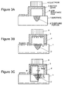
- Figure 3 is a sectional view of an optical modulator according to this embodiment.
- Figure 3A shows a case where there is not a temperature change and no electric charge is generated on the surface of the substrate.
- Figure 3B shows a case where an electric charge caused by a pyroelectric effect is generated on the surface of a Z-plate LiNbO 3 (LN) substrate due to variation in temperature of the substrate 1.
- the surface of the low resistance film 4 is electrically neutralized by being supplied with an electric charge which is inverse in polarity and equal in quantity to the electric charge generated in the vicinity of the surface of the substrate 1.
- an electric charge which has been left without being neutralized generates an electric field in the optical waveguide 2.
- FIG. 3C shows an equivalent circuit where the optical waveguide 2 and the buffer layer 3 are respectively CLN and CSiO 2 in capacitance, and the low resistance film 4 is R in resistance.
- the temperature shift V(t) is exponentially decreased. It is known from the expression (1) that it is effective to suppression of the temperature shift to decrease Q, increase CLN and decrease ⁇ .
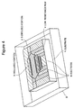
- Figure 4 shows a composition in which a light control device is housed in a package 9.
- a temperature shift in case that a temperature difference has occurred between a portion represented by an equivalent circuit, namely, a portion (hereinafter referred to as an optical device portion) consisting of the optical waveguide 2, the buffer layer 3 and the low resistance layer 4 of the light control device, and a portion (hereinafter referred to as a package portion) consisting of the other portion than the optical device portion of the light control device and a package for housing the light control device is examined in the following. Since the optical device portion and the package portion are different in heat capacity from each other, both of them do not coincide in temperature change with each other.
- T pkg (t) T 0 + ⁇ T pkg ⁇ u (t)
- T mod(t) of the optical device portion varies according to the following expression (3):
- u(t) is a unit-step function
- C pkg is the heat capacity of the package portion
- R pkg is the heat resistance (being in inverse proportion to the thermal conductivity). That is to say, the temperature change of the device depends upon the thermal time constant ⁇ pkg of the package portion.
- Figure 2 shows a perspective view of the optical device portion which is the first embodiment of the present invention.
- an optical modulator by means of a Mach-Zehnder interferometer is assumed as the light control device.
- a structure in which the composition of a package portion is not changed (namely, ⁇ pkg is fixed) is first shown as a structure for reducing a temperature shift.
- Figure 6 is a result of evaluating the temperature shift when giving a stepped temperature change to these optical modulators.
- B was decreased to 0.2 V from 1.0 V, namely, to 1/5 or less in temperature shift quantity by more lowering the low resistance film in resistance. In this manner, the temperature shift can be suppressed by reducing R.
- a temperature shift is suppressed by reducing R.
- a film forming method for forming an amorphous semiconductor film known as a low resistance film there are a deposition method, a sputtering method, a CVD method, an MBE method and the like.
- a deposition method for forming an amorphous semiconductor film by means of a sputtering method it is effective to reduction of the resistance of a film to reduce a sputtering power or to increase a sputtering gas pressure.
- the sputtering power is distant from the optimum condition, however, many defects occur when forming a film, and as a result the reproducibility of resistance value is lowered.
- a low resistance film can be formed by means of a sputtering method.
- it is the resistance value of the low resistance film that corresponds to R of the expression (4).
- the low resistance film of this embodiment may be replaced with a low resistance film formed by means of another method than a sputtering film forming method.
- a resistance value being as low as possible is desirable, so long as the low resistance can be secured in a good reproducibility by means of a CVD method, an MBE method and the like as a film forming method.
- a CVD method, an MBE method and the like as a film forming method.
- a semiconductor film but also a conductor film or an organic-compound-based conductor film can be used as the low resistance film.
- a film thickness of at least 0.1 ⁇ m or more is needed, it is desirable that the film thickness is 0.1 ⁇ m or more.
- a film having a lower resistance than the low resistance film may be formed on the surface or inside the film.
- the loss of a light control device such as an optical modulator and the like to an applied electric signal can be suppressed by forming additionally a lower resistance film inside the film.
- an electric signal applied to an optical waveguide when controlling light in an optical modulator and the like is an electromagnetic wave of a microwave band or millimeter wave band, an electric field leaks to a domain being several ⁇ m or less under the surface of a low resistance film due to a skin effect.
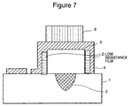
- FIG. 7 is a sectional view of an optical device showing the above-mentioned example.
- R is almost determined by the resistance value of the second low resistance film 7 and is not influenced by the low resistance film 4. Accordingly, since R is made low in resistance and at the same time the low resistance film 4 comes to have no limitation, it becomes easy to manufacture the device.
- the Q is determined by a crystal material for a substrate and is in proportion to the quantity of a spontaneous electric charge in a ferroelectric crystal.
- the quantity of a spontaneous electric charge (spontaneous polarization) and the electric power required for revealing an electro-optic effect used in controlling a wave-guided light are in proportion to each other. Therefore, it is difficult to suppress a spontaneous electric charge while controlling light with a low electric power.
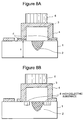
- FIGs 8A and 8B each are a sectional view of a device showing an embodiment for this purpose.
- CLN is increased by making thinner the thickness t of a substrate and making longer the length d of a low resistance film covering the substrate.
- the thickness t of a substrate is 0.8 mm or less.
- the covering length d of 2 ⁇ m or more is nearly equivalent to a domain to apply an electric field to an optical waveguide and minimizes the size of the device, this length is preferable.
- Figure 8B shows an example in which a material having a higher dielectric constant than a substrate is formed in part of the substrate and equivalently a capacitor is connected in parallel. Such compositions of Figures 8B and 8A may be used at the same time.
- a composition making k of the expression (6) be 100 or more may be adopted.
- Q/CLN cannot be controlled or in case that the structure of a device cannot be changed, since a temperature shift can be reduced by properly changing a package to house a light control device, this is an effective means.
- a method of doping a different element from the low resistance film into the film or performing a heat treatment after a film forming process is also effective to reduction of the resistance value.
- This method is well known as a method for controlling the resistance value of a semiconductor film.
- Doping may be to provide a film forming material directly with Ge, B, P or the like for example, and may be to apply an ion implantation method to a formed film itself. From a viewpoint of reproducibility of the resistance value of a film, it is more effective to apply a doping process to a film forming material.
- the resistance value of a film may not become uniform.
- the uniformity of a film is improved by heating the formed film in a pure gas atmosphere or in vacuum at a temperature of 100 to 300°C for several hours. Particularly when using an inert gas a surface reaction is also suppressed in a heating process. And it is possible also to control the resistance value by a heat treatment after a film forming process. And it is effective to reduction of the resistance value also to give an electromagnetic-wave energy such as an electron beam, ultraviolet rays and the like to the surface of a low resistance film. And it is effective to reduction of the resistance value also to generate defects at the beginning of forming a film by roughening uniformly the ground face by means of etching or a chemical reaction prior to forming a low resistance film.
- a semiconductor material such as Si, Ge or the like, a conductor material such as ITO and an organic-compound-based conductive material can be used as the low resistance material.
- the film forming can be performed by means of a process of CVD, sputtering, dip-coating, deposition, MBE and the like.
- a structure for reducing CSiO 2 is also effective to reduction of a temperature shift.
- the CSiO 2 is in proportion to the dielectric constant of a buffer layer and the area of an electrode, and is in inverse proportion to the spacing between the electrodes.
- the dielectric constant can be reduced to 4 or less by properly selecting a film forming condition and a material.
- the length of an electrode length of a device is in proportion to the area of the electrode, the area of the electrode is preferably 0.42 mm2 or less. Since CSiO 2 is reduced when the thickness of a buffer layer is made thicker, it is possible also to form a buffer layer of 0.9 ⁇ m or more in thickness.
- ⁇ of the expression (3) is 5 seconds or less.
- the optical modulator evaluated in Figure 6 is considered as a general optical device.
- the time constant of about 5 seconds is obtained and an electric charge generated on the surface of the substrate in case of receiving a temperature change of about 1 °C/minute can be neutralized.
- ⁇ needs to be made smaller.
- the ratio of a time constant to a temperature change rate is preferable thanks to making it possible to reduce the temperature shift in a similar manner.
- a material for a package can be composed of a material of 0.52 J ⁇ K -1 ⁇ g -1 at 373 K in specific heat at constant pressure.
- the heat capacity CPC of the package portion can be made large by making large the specific heat of a material for the package.
- the maximum value of a temperature shift is decreased according to the expression (6).
- some of materials of inorganic compound or liquid such as oil may have a heat capacity being 10 or more times larger than metal and may be effective to suppression of a temperature shift.
- a heat resistance is the inverse number of a thermal conductivity
- a thermal conductivity of 16.5 W ⁇ m -1 ⁇ K -1 or less at 300 K is effective to reduction of a temperature shift.
- a material being lower in thermal conductivity than metal by one digit or more and such a material reduces a temperature shift according to the expression (6).
- the temperature shifts of equivalent devices mounted in packages being different in ⁇ pkg were evaluated.
- Figure 9 shows a result of evaluation of temperature shifts in a temperature change from 65 °C to 85°C, and the axis of abscissas represents time and the axis of ordinates represents the quantity of a temperature shift.
- the mass of a package corresponding to an evaluation result shown by B is about 10 times the mass of a package corresponding to A.
- Time constant ⁇ pkg of the package portion is in proportion to (specific heat)/(thermal conductivity) and B is about 12 times larger in the value of this ratio than A. From Figure 9, a package being larger in this ratio is reduced more in temperature shift and this coincides with a result expected from the expression (6).
- a package formed out of unit elements each being in the shape of a sphere has a ratio of surface area to volume of about 2.2
- a package formed out of only cubic unit elements has a ratio of 6 as this ratio and becomes two or more times in heat radiation efficiency. Therefore, when a package contains cubic elements as its components, its ⁇ pkg becomes larger.
- a method for the surface area can utilize the structure of a heat sink portion used in a power supply circuit, a microprocessor and the like.
- the present invention can be implemented in an optical modulator, an optical switch, an optical filter, an optical isolator, an optical coupler, an optical sensor and the like which use an optical waveguide. It is apparent that the present invention is not limited to the above-mentioned embodiments, but can be properly modified in the scope of the technical idea of the present invention.
- a light control device consisting of an optical waveguide formed on the surface of a ferroelectric crystal substrate
- a composition in which the resistance value, capacity, heat capacity and thermal conductivity of each of its components are controlled.
- Such a composition can neutralize in a short time an electric charge generated on the surface of a substrate when the substrate varies in temperature, and can suppress an operation point shift at the time of change in temperature.
Landscapes
- Physics & Mathematics (AREA)
- Nonlinear Science (AREA)
- Chemical & Material Sciences (AREA)
- Engineering & Computer Science (AREA)
- Ceramic Engineering (AREA)
- Crystallography & Structural Chemistry (AREA)
- General Physics & Mathematics (AREA)
- Optics & Photonics (AREA)
- Optical Modulation, Optical Deflection, Nonlinear Optics, Optical Demodulation, Optical Logic Elements (AREA)
- Optical Integrated Circuits (AREA)
Applications Claiming Priority (2)
| Application Number | Priority Date | Filing Date | Title |
|---|---|---|---|
| JP23834598A JP3237620B2 (ja) | 1998-08-25 | 1998-08-25 | 光制御デバイスおよびその製造方法 |
| JP23834598 | 1998-08-25 |
Publications (2)
| Publication Number | Publication Date |
|---|---|
| EP0982619A2 true EP0982619A2 (de) | 2000-03-01 |
| EP0982619A3 EP0982619A3 (de) | 2004-06-16 |
Family
ID=17028828
Family Applications (1)
| Application Number | Title | Priority Date | Filing Date |
|---|---|---|---|
| EP99116640A Withdrawn EP0982619A3 (de) | 1998-08-25 | 1999-08-25 | Vorrichtung zur steuerung des lichts sowie das Herstellungsverfahren derselben |
Country Status (4)
| Country | Link |
|---|---|
| US (1) | US6385360B1 (de) |
| EP (1) | EP0982619A3 (de) |
| JP (1) | JP3237620B2 (de) |
| KR (1) | KR100364033B1 (de) |
Cited By (1)
| Publication number | Priority date | Publication date | Assignee | Title |
|---|---|---|---|---|
| WO2005098493A1 (en) * | 2004-04-02 | 2005-10-20 | Northrop Grumman Corporation | Implementation of one or more optical waveguides in reduced optical material |
Families Citing this family (7)
| Publication number | Priority date | Publication date | Assignee | Title |
|---|---|---|---|---|
| WO2002097521A1 (fr) * | 2001-05-25 | 2002-12-05 | Anritsu Corporation | Dispositif de modulation optique presentant d'excellentes caracteristiques electriques grace a une restriction efficace du transfert de chaleur |
| US7019882B1 (en) | 2002-03-21 | 2006-03-28 | Lockheed Martin Corporation | Generation of M-ary digital signaling constellations directly at lightwave frequencies |
| CN1300957C (zh) * | 2003-09-18 | 2007-02-14 | 电子科技大学 | 超宽带集成光波导微波副载波电磁波接收器 |
| JP2013037243A (ja) * | 2011-08-09 | 2013-02-21 | Fujitsu Optical Components Ltd | 光変調器 |
| WO2021065578A1 (ja) * | 2019-10-04 | 2021-04-08 | 国立大学法人東京工業大学 | 光変調素子 |
| CN110989214B (zh) * | 2019-12-23 | 2022-12-27 | 武汉邮电科学研究院有限公司 | 一种电光调制器 |
| JP2022143378A (ja) | 2021-03-17 | 2022-10-03 | 富士通オプティカルコンポーネンツ株式会社 | 変調信号の制御装置 |
Family Cites Families (9)
| Publication number | Priority date | Publication date | Assignee | Title |
|---|---|---|---|---|
| US5153930A (en) | 1990-01-04 | 1992-10-06 | Smiths Industries Aerospace & Defense Systems, Inc. | Device employing a substrate of a material that exhibits the pyroelectric effect |
| JP2867560B2 (ja) * | 1990-03-02 | 1999-03-08 | 富士通株式会社 | 光導波路デバイス |
| JPH0419714A (ja) * | 1990-05-15 | 1992-01-23 | Oki Electric Ind Co Ltd | 光デバイス |
| JPH0720176A (ja) * | 1993-07-07 | 1995-01-24 | Tokin Corp | 光電界センサ |
| JP3253815B2 (ja) | 1994-10-19 | 2002-02-04 | 日本パーオキサイド株式会社 | ステンレス鋼製器材の洗浄方法、及びその洗浄剤 |
| JP2894961B2 (ja) * | 1994-11-18 | 1999-05-24 | 日本電気株式会社 | 光制御デバイス |
| JPH09236782A (ja) * | 1996-02-29 | 1997-09-09 | Kyocera Corp | 光導波路デバイス |
| JPH09258152A (ja) * | 1996-03-21 | 1997-10-03 | Tdk Corp | 導波路型光デバイス |
| JP2850899B2 (ja) | 1997-04-21 | 1999-01-27 | 日本電気株式会社 | 光制御デバイス |
-
1998
- 1998-08-25 JP JP23834598A patent/JP3237620B2/ja not_active Expired - Fee Related
-
1999
- 1999-08-23 US US09/378,721 patent/US6385360B1/en not_active Expired - Fee Related
- 1999-08-25 EP EP99116640A patent/EP0982619A3/de not_active Withdrawn
- 1999-08-25 KR KR1019990035315A patent/KR100364033B1/ko not_active Expired - Fee Related
Cited By (2)
| Publication number | Priority date | Publication date | Assignee | Title |
|---|---|---|---|---|
| WO2005098493A1 (en) * | 2004-04-02 | 2005-10-20 | Northrop Grumman Corporation | Implementation of one or more optical waveguides in reduced optical material |
| US7903920B2 (en) | 2004-04-02 | 2011-03-08 | Northrop Grumman Guidance And Electronics Company, Inc. | Implementation of one or more optical waveguides in reduced optical material |
Also Published As
| Publication number | Publication date |
|---|---|
| JP3237620B2 (ja) | 2001-12-10 |
| KR100364033B1 (ko) | 2002-12-11 |
| KR20000017501A (ko) | 2000-03-25 |
| EP0982619A3 (de) | 2004-06-16 |
| US6385360B1 (en) | 2002-05-07 |
| JP2000066157A (ja) | 2000-03-03 |
Similar Documents
| Publication | Publication Date | Title |
|---|---|---|
| EP0554593B1 (de) | Verfahren zur Herstellung einer Vorrichtung, die ein Substrat mit pyroelektrischem Effekt benutzt | |
| JP2555942B2 (ja) | 光制御デバイス | |
| CA2118272A1 (en) | Electrooptic device structure and method for reducing thermal effects in optical waveguide modulators | |
| US6385360B1 (en) | Light control device and a method for manufacturing the same | |
| JP4642356B2 (ja) | ニオブ酸リチウムデバイスを安定化させるための緩衝層構造 | |
| JPH08146367A (ja) | 光制御デバイス | |
| JP2005515485A6 (ja) | ニオブ酸リチウムデバイスを安定化させるための緩衝層構造 | |
| JP2005515499A6 (ja) | ニオブ酸リチウムデバイスを安定化させるための緩衝層構造 | |
| JPH07120631A (ja) | 光導波路型部品 | |
| JPH0675195A (ja) | 光制御デバイス | |
| JPH0561009A (ja) | 光導波路素子 | |
| EP1348992B1 (de) | Optisches wellenleiterbauelement | |
| EP1463973B1 (de) | Pufferschichtstruktur zur stabilisierung einer lithiumniobat-vorrichtung | |
| JP3139712B2 (ja) | 光制御デバイス | |
| EP1687671A1 (de) | Polarisationsunabhängiger elektrooptischer modulator | |
| JP3487664B2 (ja) | 光機能デバイス及びその駆動方法 | |
| JPH0815657A (ja) | 導波路型電気光学素子 | |
| JP2730465B2 (ja) | 光制御デバイスとその製造方法 | |
| JP2503880B2 (ja) | 光制御デバイスの製造方法 | |
| JP2026055668A (ja) | 位相シフター、位相シフト方法、およびマッハツェンダー型光干渉計 | |
| Nagata | Reliability of Lithium Niobate Modulators | |
| JPH07152051A (ja) | 光導波路素子 | |
| JPH063710A (ja) | 光制御デバイス及びその製造方法 | |
| JPH05289032A (ja) | 光デバイスの制御法 |
Legal Events
| Date | Code | Title | Description |
|---|---|---|---|
| PUAI | Public reference made under article 153(3) epc to a published international application that has entered the european phase |
Free format text: ORIGINAL CODE: 0009012 |
|
| AK | Designated contracting states |
Kind code of ref document: A2 Designated state(s): AT BE CH CY DE DK ES FI FR GB GR IE IT LI LU MC NL PT SE |
|
| AX | Request for extension of the european patent |
Free format text: AL;LT;LV;MK;RO;SI |
|
| PUAL | Search report despatched |
Free format text: ORIGINAL CODE: 0009013 |
|
| AK | Designated contracting states |
Kind code of ref document: A3 Designated state(s): AT BE CH CY DE DK ES FI FR GB GR IE IT LI LU MC NL PT SE |
|
| AX | Request for extension of the european patent |
Extension state: AL LT LV MK RO SI |
|
| 17P | Request for examination filed |
Effective date: 20041110 |
|
| AKX | Designation fees paid |
Designated state(s): DE GB |
|
| STAA | Information on the status of an ep patent application or granted ep patent |
Free format text: STATUS: THE APPLICATION IS DEEMED TO BE WITHDRAWN |
|
| 18D | Application deemed to be withdrawn |
Effective date: 20060705 |