EP0982622A2 - Dispositif à cristal liquide et appareillage électronique le comprenant - Google Patents
Dispositif à cristal liquide et appareillage électronique le comprenant Download PDFInfo
- Publication number
- EP0982622A2 EP0982622A2 EP99306617A EP99306617A EP0982622A2 EP 0982622 A2 EP0982622 A2 EP 0982622A2 EP 99306617 A EP99306617 A EP 99306617A EP 99306617 A EP99306617 A EP 99306617A EP 0982622 A2 EP0982622 A2 EP 0982622A2
- Authority
- EP
- European Patent Office
- Prior art keywords
- liquid crystal
- panel
- crystal device
- main substrate
- light guide
- Prior art date
- Legal status (The legal status is an assumption and is not a legal conclusion. Google has not performed a legal analysis and makes no representation as to the accuracy of the status listed.)
- Withdrawn
Links
Images



Classifications
-
- G—PHYSICS
- G02—OPTICS
- G02F—OPTICAL DEVICES OR ARRANGEMENTS FOR THE CONTROL OF LIGHT BY MODIFICATION OF THE OPTICAL PROPERTIES OF THE MEDIA OF THE ELEMENTS INVOLVED THEREIN; NON-LINEAR OPTICS; FREQUENCY-CHANGING OF LIGHT; OPTICAL LOGIC ELEMENTS; OPTICAL ANALOGUE/DIGITAL CONVERTERS
- G02F1/00—Devices or arrangements for the control of the intensity, colour, phase, polarisation or direction of light arriving from an independent light source, e.g. switching, gating or modulating; Non-linear optics
- G02F1/01—Devices or arrangements for the control of the intensity, colour, phase, polarisation or direction of light arriving from an independent light source, e.g. switching, gating or modulating; Non-linear optics for the control of the intensity, phase, polarisation or colour
- G02F1/13—Devices or arrangements for the control of the intensity, colour, phase, polarisation or direction of light arriving from an independent light source, e.g. switching, gating or modulating; Non-linear optics for the control of the intensity, phase, polarisation or colour based on liquid crystals, e.g. single liquid crystal display cells
- G02F1/133—Constructional arrangements; Operation of liquid crystal cells; Circuit arrangements
- G02F1/1333—Constructional arrangements; Manufacturing methods
- G02F1/133308—Support structures for LCD panels, e.g. frames or bezels
-
- G—PHYSICS
- G02—OPTICS
- G02F—OPTICAL DEVICES OR ARRANGEMENTS FOR THE CONTROL OF LIGHT BY MODIFICATION OF THE OPTICAL PROPERTIES OF THE MEDIA OF THE ELEMENTS INVOLVED THEREIN; NON-LINEAR OPTICS; FREQUENCY-CHANGING OF LIGHT; OPTICAL LOGIC ELEMENTS; OPTICAL ANALOGUE/DIGITAL CONVERTERS
- G02F1/00—Devices or arrangements for the control of the intensity, colour, phase, polarisation or direction of light arriving from an independent light source, e.g. switching, gating or modulating; Non-linear optics
- G02F1/01—Devices or arrangements for the control of the intensity, colour, phase, polarisation or direction of light arriving from an independent light source, e.g. switching, gating or modulating; Non-linear optics for the control of the intensity, phase, polarisation or colour
- G02F1/13—Devices or arrangements for the control of the intensity, colour, phase, polarisation or direction of light arriving from an independent light source, e.g. switching, gating or modulating; Non-linear optics for the control of the intensity, phase, polarisation or colour based on liquid crystals, e.g. single liquid crystal display cells
- G02F1/133—Constructional arrangements; Operation of liquid crystal cells; Circuit arrangements
- G02F1/1333—Constructional arrangements; Manufacturing methods
- G02F1/1335—Structural association of cells with optical devices, e.g. polarisers or reflectors
-
- G—PHYSICS
- G02—OPTICS
- G02F—OPTICAL DEVICES OR ARRANGEMENTS FOR THE CONTROL OF LIGHT BY MODIFICATION OF THE OPTICAL PROPERTIES OF THE MEDIA OF THE ELEMENTS INVOLVED THEREIN; NON-LINEAR OPTICS; FREQUENCY-CHANGING OF LIGHT; OPTICAL LOGIC ELEMENTS; OPTICAL ANALOGUE/DIGITAL CONVERTERS
- G02F1/00—Devices or arrangements for the control of the intensity, colour, phase, polarisation or direction of light arriving from an independent light source, e.g. switching, gating or modulating; Non-linear optics
- G02F1/01—Devices or arrangements for the control of the intensity, colour, phase, polarisation or direction of light arriving from an independent light source, e.g. switching, gating or modulating; Non-linear optics for the control of the intensity, phase, polarisation or colour
- G02F1/13—Devices or arrangements for the control of the intensity, colour, phase, polarisation or direction of light arriving from an independent light source, e.g. switching, gating or modulating; Non-linear optics for the control of the intensity, phase, polarisation or colour based on liquid crystals, e.g. single liquid crystal display cells
- G02F1/133—Constructional arrangements; Operation of liquid crystal cells; Circuit arrangements
- G02F1/1333—Constructional arrangements; Manufacturing methods
- G02F1/133308—Support structures for LCD panels, e.g. frames or bezels
- G02F1/133317—Intermediate frames, e.g. between backlight housing and front frame
-
- G—PHYSICS
- G02—OPTICS
- G02F—OPTICAL DEVICES OR ARRANGEMENTS FOR THE CONTROL OF LIGHT BY MODIFICATION OF THE OPTICAL PROPERTIES OF THE MEDIA OF THE ELEMENTS INVOLVED THEREIN; NON-LINEAR OPTICS; FREQUENCY-CHANGING OF LIGHT; OPTICAL LOGIC ELEMENTS; OPTICAL ANALOGUE/DIGITAL CONVERTERS
- G02F1/00—Devices or arrangements for the control of the intensity, colour, phase, polarisation or direction of light arriving from an independent light source, e.g. switching, gating or modulating; Non-linear optics
- G02F1/01—Devices or arrangements for the control of the intensity, colour, phase, polarisation or direction of light arriving from an independent light source, e.g. switching, gating or modulating; Non-linear optics for the control of the intensity, phase, polarisation or colour
- G02F1/13—Devices or arrangements for the control of the intensity, colour, phase, polarisation or direction of light arriving from an independent light source, e.g. switching, gating or modulating; Non-linear optics for the control of the intensity, phase, polarisation or colour based on liquid crystals, e.g. single liquid crystal display cells
- G02F1/133—Constructional arrangements; Operation of liquid crystal cells; Circuit arrangements
- G02F1/1333—Constructional arrangements; Manufacturing methods
- G02F1/1335—Structural association of cells with optical devices, e.g. polarisers or reflectors
- G02F1/1336—Illuminating devices
- G02F1/133615—Edge-illuminating devices, i.e. illuminating from the side
-
- G—PHYSICS
- G02—OPTICS
- G02F—OPTICAL DEVICES OR ARRANGEMENTS FOR THE CONTROL OF LIGHT BY MODIFICATION OF THE OPTICAL PROPERTIES OF THE MEDIA OF THE ELEMENTS INVOLVED THEREIN; NON-LINEAR OPTICS; FREQUENCY-CHANGING OF LIGHT; OPTICAL LOGIC ELEMENTS; OPTICAL ANALOGUE/DIGITAL CONVERTERS
- G02F1/00—Devices or arrangements for the control of the intensity, colour, phase, polarisation or direction of light arriving from an independent light source, e.g. switching, gating or modulating; Non-linear optics
- G02F1/01—Devices or arrangements for the control of the intensity, colour, phase, polarisation or direction of light arriving from an independent light source, e.g. switching, gating or modulating; Non-linear optics for the control of the intensity, phase, polarisation or colour
- G02F1/13—Devices or arrangements for the control of the intensity, colour, phase, polarisation or direction of light arriving from an independent light source, e.g. switching, gating or modulating; Non-linear optics for the control of the intensity, phase, polarisation or colour based on liquid crystals, e.g. single liquid crystal display cells
- G02F1/133—Constructional arrangements; Operation of liquid crystal cells; Circuit arrangements
- G02F1/1333—Constructional arrangements; Manufacturing methods
- G02F1/1345—Conductors connecting electrodes to cell terminals
- G02F1/13452—Conductors connecting driver circuitry and terminals of panels
-
- G—PHYSICS
- G02—OPTICS
- G02F—OPTICAL DEVICES OR ARRANGEMENTS FOR THE CONTROL OF LIGHT BY MODIFICATION OF THE OPTICAL PROPERTIES OF THE MEDIA OF THE ELEMENTS INVOLVED THEREIN; NON-LINEAR OPTICS; FREQUENCY-CHANGING OF LIGHT; OPTICAL LOGIC ELEMENTS; OPTICAL ANALOGUE/DIGITAL CONVERTERS
- G02F2201/00—Constructional arrangements not provided for in groups G02F1/00 - G02F7/00
- G02F2201/46—Fixing elements
- G02F2201/465—Snap -fit
Definitions
- the present invention relates to a liquid crystal device including a liquid crystal sealed between a pair of substrates and also to an electronic apparatus constructed using such a liquid crystal device.
- liquid crystal devices are used as image display units in a wide variety of devices such as portable telephones, portable electronic terminals, electronic personal organizers, and other electronic devices.
- Liquid crystal devices are produced by bonding a pair of substrates to each other and enclosing a liquid crystal within a space called a cell gap formed between the substrates.
- the substrates are each formed of, for example, a transparent substrate, and transparent electrodes are formed on both substrates such that the transparent electrodes face each other.
- Polarizers are disposed, as necessary, on the outer surfaces of the pair of substrates.
- a color filter is disposed on the inner surface of one substrate.
- the alignment of the liquid crystal is controlled by varying the voltage applied between the electrodes opposing each other via the liquid crystal so as to modulate light supplied to the liquid crystal, thereby displaying an image such as a character, numeral, or pattern.
- the control of the voltage applied between the opposing electrodes is accomplished by a liquid crystal driving integrated circuit (IC) electrically connected to the electrodes.
- IC liquid crystal driving integrated circuit
- a light guide 87 serving as a panel supporting member is disposed on a main substrate 83 which is one component of an electronic apparatus such as a portable telephone, and a liquid crystal panel 82 is placed on the light guide 87. Furthermore, a cover 80 is placed thereon from above and the cover 80 is connected to the main substrate 83 by engaging an engagement lug 81 formed at the bottom of the cover 80 into an engagement hole 85 thereby fixing the liquid crystal panel 82 at a predetermined location on the main substrate 83.
- the cover 80 is usually formed of a metal such as stainless steel.
- the cover 80 is provided primarily to fix the liquid crystal panel 82 to the light guide 87 in such a manner that the liquid crystal panel 82 and the light guide 87 are combined together in an integral fashion, and also to apply a uniform pressure to an elastic connector 84 disposed between the liquid crystal panel 82 and the main substrate 83, thereby electrically conductively connecting a panel-side electrode terminal formed on the liquid crystal panel 82 to a main substrate-side electrode terminal formed on the main substrate 83.
- the cover employed in the conventional liquid crystal device results in an increase in cost and also an increase in the number of assembly steps.
- a liquid crystal device having a structure which allows a liquid crystal panel to be fixed using only a light guide (panel supporting member) without necessitating an additional member such as a cover, thereby achieving a reduction in cost.
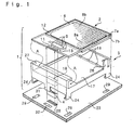
- Fig. 1 illustrates, in an exploded fashion, an embodiment of a liquid crystal device according to the present invention
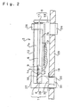
- Fig. 2 is a side view illustrating, in a partially cutaway fashion, the liquid crystal device in an assembled state.
- the liquid crystal device 1 according to the present embodiment includes a liquid crystal panel 2, a backlight unit 3, and an elastic connector 4.
- the liquid crystal panel 2 includes a pair of substrates 7a and 7b connected to each other via a sealing material 6. These substrate 7a and 7b are formed of a transparent material such as glass, plastic. Polarizers 12 are bonded to the respective outer surfaces of these substrates.
- Linear transparent electrodes 8a are formed on the inner surface of one substrate 7a and linear electrodes 8b extending in a direction perpendicular to the electrodes 8a are formed on the inner surface of the other substrate 7b.
- These electrodes 8a and 8b are formed, for example, of ITO (indium tin oxide).
- ITO indium tin oxide
- One pixel for displaying an image is formed at each intersection between the electrodes 8a and 8b.
- the shape of the electrodes 8a and 8b is not limited to being linear, and they may be constructed in another proper form such as a mark or a pattern.
- One substrate 7a has a protruding part extending outward beyond an edge of the opposite substrate 7b.
- a plurality of IC output terminals 9 and a plurality of panel-side electrode terminals 11 are formed using, for example, ITO on the surface of the protruding part.
- the plurality of IC output terminals 9 include those continuously extending from electrodes 8a and those connected to electrodes 8b via conductive elements.
- the electrodes 8a, 8b, the IC output terminals 9, and the panel-side terminals 11 are formed in such a manner that a great number of these terminals are arranged at very small intervals on each substrate.
- these terminals are schematically represented in expanded intervals for a better understanding of their structure.
- connections between the IC output terminals 9 and the electrodes 8a and 8b are not shown in Fig. 1.
- a liquid crystal driving IC 13 is disposed on the protruding part of the substrate 7a. More specifically, as shown in Fig. 2, bumps 14 on the liquid crystal driving IC 13 are conductively connected to the IC output terminals 9 and the panel-side electrode terminals 11 via an ACF (anisotropic conductive film) 16.
- ACF anisotropic conductive film
- the ACF 16 is a conductive high-polymer film used to make conductive connections between pairs of terminals in a batch fashion, as is known.
- the ACF 16 may be formed, for example, by dispersing conductive particles within a thermoplastic resin film or a thermosetting resin film. Conductive connections in a particular single direction can be realized by connecting the ACF 16 by means of thermocompression bonding.
- the backlight unit 3 includes a light guide 17 and a plurality of LEDs (light emitting diodes) 18 disposed on one end of the light guide 17. At the other end of the light guide 17, a guide hole 19 for guiding the elastic connector 4 is formed. This guide hole 19 is formed to have a size that can snugly receive the elastic connector 4.
- Engagement pawls 24 serving as engagement members are formed in respective four corners on the bottom of the light guide 17. In Fig. 1, only three visible engagement pawls 24 are illustrated, and one engagement pawl hidden behind the light guide 17 is not shown.
- a fixing pawl 26 serving as a fixing member is formed on each of two opposite sides of the light guide 17, at locations near the end on which LEDs 18 are disposed. In Fig. 1, only one fixing pawl 26 is illustrated and the remaining one hidden behind the liquid crystal panel 2 is not shown.
- a pressure pawl 31 serving as a uniformly pressing member is formed on the lower surface of the light guide 17, at the end where the guide hole 19 is formed and at a location close to the guide hole 19.
- a protruding part 27 protruding toward the inside of light guide 17 is formed on the upper surface of the light guide 17, at the end where the guide hole 19 is formed.
- a space is formed between the protruding part 27 and the upper surface of the light guide 17 such that an end portion of the liquid crystal panel 2 can be inserted into that space.
- the engagement pawls 24, the fixing pawls 26, and the pressure pawl 31 each have, at their top, a projection or a latching part in the form of a pawl projecting inwardly to latch a target object. With these latch parts, the light guide 17 and the target object are engaged and connected with each other.
- the light guide 17 may be formed of either (1) a transparent resin such as an acrylic resin, a polycarbonate resin, or amorphous polyolefin resins; (2) a transparent inorganic material such as glass; or (3) a mixture of any of the above-described materials.
- the light guide 17 may be formed by any of methods: (1) injection molding; (2) a technique using photo-curing of a resin; (3) etching; or (4) adhesively bonding a film to a surface of a plate made of a transparent resin or glass.
- the engagement pawls 24, the fixing pawls 26, and the protruding part 27 are formed integrally with the light guide 17.
- the fixing pawls 26, and the protruding part 27 may be connected into a single piece using an adhesive or other connecting means.
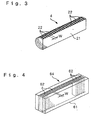
- the elastic connector 4 comprises, as shown in Fig. 3, an elastic base 21 formed in the shape of a semicircle or the letter "U” rotated on its side in cross section using a material which is elastic and electrically insulating such as silicone rubber, and a large number of conductive parts 22 are formed so as to be parallel to each other on the circumferential surface of the elastic base 21. All adjacent conductive parts 22 are spaced from each other by, for example, 15 ⁇ m to 25 ⁇ m and are electrically isolated from each other by the elastic material.
- symbol "W” denotes the distance or pitch between adjacent conductive parts 22. The pitch is generally set to a value in a range of from 30 ⁇ m to 50 ⁇ m.
- reference numeral 23 denotes a main substrate on which the liquid crystal device 1 is mounted.
- the main substrate 23 is one of the parts constituting an electronic apparatus such as a portable telephone.
- the main substrate 23 has engagement holes 29 for receiving the corresponding engagement pawls 24 formed in the respective four corners on the lower surface of the light guide 17, and also has a pressure pawl engagement hole 32 for receiving the pressure pawl 31 formed on the light guide 17.
- the elastic connector 4 is pressed with a predetermined uniform pressure over the length thereof by the end part, on the side where the panel-side electrode terminals 11 are formed, of the liquid crystal panel 2 against the surface of the main substrate 23 by means of engagement between the pressure pawl 31 and the pressure pawl engagement hole 32. This ensures that the panel-side electrode terminals 11 are conductively connected in a highly reliable fashion to the main substrate-side electrode terminals 28 through the conductive parts 22 of the elastic connector 4. By disposing the pressure pawl 31 in close proximity to the elastic connector 4, it becomes possible to uniformly apply pressure to the elastic connector 4, and thus the elastic connector 4 can provide connections with high connection reliability.
- the liquid crystal driving IC 13 controls the voltages applied to the electrodes 8a and 8b of the liquid crystal panel 2.
- light transmitted from the LED 18 to the liquid crystal panel 2 through the light guide 17 is modulated on a pixel-by-pixel basis by the above described voltage control so as to display an image such as a character and a number in the display area of the liquid crystal panel 2.
- the light guide 17 serving as the panel supporting member is fixed to the main substrate 23 by the engagement pawls 24 serving as the engagement members and the liquid crystal panel 2 is supported by the light guide 17 so as to mount the liquid crystal panel 2 at the predetermined position above the main substrate 23.
- the pressure pawl 31 serving as the uniformly pressing member is formed in the light guide 17 so that pressure is uniformly applied to the elastic connector 4 thereby ensuring that highly-reliable conductive connections are achieved between the panel-side electrode terminals 11 and the main substrate-side electrode terminals 28.
- Such highly-reliable conductive connections are achieved using only the light guide 17 without necessitating a cover (such as a cover 80 shown in Fig. 8) which is used conventionally. This allows reductions in both component cost and assembly cost.
- Fig. 4 shows a rubber connector 64 which is a modification of the elastic connector for use in the present invention.
- This rubber connector 64 comprises an elastic base 61 formed in a generally rectangular shape using a material which is elastic and electrically insulating, such as silicone rubber, and a large number of conductive parts 62 disposed parallel to each other inside the elastic base 61. The upper and lower ends of the respective conductive parts 62 are exposed to the outside of the elastic base 61. Adjacent conductive parts 62 are all spaced from each other by the pitch W, for example, 30 ⁇ m to 50 ⁇ m and are electrically isolated from each other by the elastic material.
- each of the panel-side electrode terminals 11 on the side of the liquid crystal panel 2 and each of the main substrate-side electrode terminals 28 on the side of the main substrate 23 are respectively conductively connected to each other through the respective conductive parts 62 of the rubber connector 64.
- Fig. 5 illustrates a spring connector 74 which is another modification of the elastic connector for use in the present invention.
- This spring connector 74 can be used instead of the rubber connector 4 shown in Fig. 3 or the rubber connector 64 shown in Fig. 4.
- the spring connector 74 shown in Fig. 5 is formed of a plurality of spring terminals 72 arranged parallel to each other and a case 78 in which the spring terminals 72 are disposed.
- Each spring terminal 72 includes a fixed terminal 72a extending to the outside of the case 78 from its one side and a movable terminal 72b extending to the outside of the case 78 from its upper surface.
- the movable terminals 72b have elasticity which allow them to move up and down in Fig. 5.
- the spring connector 74 is fixed on the main substrate 23 such that the fixed terminals 72a are conductively connected via solder or the like to the main substrate-side electrode terminals 28 on the main substrate 23 (refer to Fig. 1). If the backlight unit 3 and the liquid crystal panel 2 are mounted on the main substrate 23 on which the spring connector 74 is disposed, then the panel-side electrode terminals 11 of the liquid crystal panel 2 come into contact with the movable terminals 72b of the spring connector 74, and the panel-side electrode terminals 11 press the movable terminals 72b downward. Because the spring terminal 72 itself has elastic properties, the movable terminals 72b press the panel-side electrode terminals 11 by means of their elastic force. This ensures that highly-reliable conductive connections are provided between the movable terminals 72b and the panel-side electrode terminals 11.
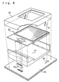
- Fig. 6 illustrates another embodiment of a liquid crystal device according to the present invention.
- the liquid crystal device 41 shown in Fig. 6 is different from the liquid crystal device 1 shown in Fig. 1 in that a modification is made to the uniformly pressing member for making the pressure which is applied to the elastic connector uniform when the liquid crystal device is assembled on the main substrate.
- elements similar to those in Fig. 1 are denoted by similar reference numerals and they are not described in further detail here.
- the uniformly pressing member is realized using the pressure pawl 31 having the latching part formed at the end thereof and the pressure pawl engagement hole 32 for engagement with the latching part.
- the uniformly pressing member is realized by a protruding part 42 formed on the light guide 17 in close proximity to the guide hole 19, a screw 43, and a threaded hole 44 formed in the main substrate 23.
- a through-hole 46 having a size capable of receiving the screw 43 is formed in the protruding part 42 so that after passing the screw 43 through the through-hole 46, the screw 43 can be screwed into the threaded hole 44.
- the protruding part 42 is formed in close proximity to the guide hole 19 so that after inserting the elastic connector 4 in the guide hole 19 and then attaching the liquid crystal panel 2 to the upper surface of the light guide 17 and finally mounting the light guide 17 on the main substrate 23, if the screw 43 is screwed into the threaded hole 44 via the through-hole 46, then pressure is applied uniformly to the elastic connector 4.
- uniform application of pressure can be achieved using only the light guide 17 without necessitating a cover (such as a cover 80 shown in Fig. 8) which is used conventionally. This allows reductions in both component cost and assembly cost.
- Fig. 7 illustrates a portable telephone which is an embodiment of an electronic apparatus according to the present invention.
- the portable telephone 50 comprises an antenna 51, a loudspeaker 52, a liquid crystal device 1, key switches 53, a microphone 54, and the like, wherein these components are disposed in a case 56.
- a control circuit board 57 on which a control circuit for controlling the above-described components is mounted.
- the liquid crystal device 1 described above with reference to Fig. 1 may be employed herein as the liquid crystal device 1.
- signals input via the microphone 54 or key switches 53, and signals received via the antenna 51 are applied to the control circuit on the control circuit board 57.
- the control circuit displays an image such as a numeral, character, or pattern in the display area of the liquid crystal device 1.
- the control circuit also transmits data via the antenna 51.
- the light guide 17 serving as the panel supporting member is fixed to the main substrate 23 by the engagement pawls 24 serving as the engagement members and the liquid crystal panel 2 is supported by the light guide 17 so as to mount the liquid crystal panel 2 at the predetermined position above the main substrate 23. Furthermore, because the pressure pawl 31 serving as the uniformly pressing member is formed on the light guide 17, pressure is uniformly applied to the elastic connector 4, thereby ensuring that highly-reliable conductive connections are achieved between the panel-side electrode terminals 11 and the main substrate-side electrode terminals 28. Such highly-reliable conductive connections are achieved using only the light guide 17 without necessitating a cover (such as a cover 80 shown in Fig. 8) which is used conventionally. This allows reductions in both component cost and assembly cost.
- liquid crystal device of the COG (chip-on-glass) type in which a liquid crystal driving integrated circuit is directly mounted on the substrate 7a of the liquid crystal panel 2, the invention may also be applied to a liquid crystal device having another structure.
- liquid crystal device according to the present invention is applied to a portable telephone taken as an example of an electronic apparatus
- the liquid crystal device according to the present invention may also be applied to other types of electronic apparatus such as a portable information terminal, an electronic personal organizer, a viewfinder of a video camera, and the like.
- the liquid crystal device 1 which is of the transmissive type using the backlight device 3 serving as the illumination device.
- a reflective liquid crystal device is also known which displays an image by means of reflection of external light such as solar light without using an illumination device.
- no light guide is used and thus the panel supporting member is formed of a component other than the light guide, although it is possible to provide a member dedicated to supporting the liquid crystal panel.
- the present invention has various advantages. That is, in the liquid crystal device and electronic apparatus according to the present invention, the uniformly pressing member formed on the panel supporting member allows pressure to be applied uniformly to the elastic connector, thereby ensuring that highly-reliable conductive connections are achieved between the panel-side electrode terminals and the main substrate-side electrode terminals. Such highly-reliable conductive connections can be obtained without using an additional component such as a cover, and thus reductions in both component cost and
Landscapes
- Physics & Mathematics (AREA)
- Nonlinear Science (AREA)
- Mathematical Physics (AREA)
- Chemical & Material Sciences (AREA)
- Crystallography & Structural Chemistry (AREA)
- General Physics & Mathematics (AREA)
- Optics & Photonics (AREA)
- Liquid Crystal (AREA)
- Devices For Indicating Variable Information By Combining Individual Elements (AREA)
- Light Guides In General And Applications Therefor (AREA)
Applications Claiming Priority (4)
| Application Number | Priority Date | Filing Date | Title |
|---|---|---|---|
| JP24086898 | 1998-08-26 | ||
| JP24086898 | 1998-08-26 | ||
| JP16130099 | 1999-06-08 | ||
| JP16130099A JP3728981B2 (ja) | 1998-08-26 | 1999-06-08 | 液晶装置及び電子機器 |
Publications (2)
| Publication Number | Publication Date |
|---|---|
| EP0982622A2 true EP0982622A2 (fr) | 2000-03-01 |
| EP0982622A3 EP0982622A3 (fr) | 2001-04-18 |
Family
ID=26487482
Family Applications (1)
| Application Number | Title | Priority Date | Filing Date |
|---|---|---|---|
| EP99306617A Withdrawn EP0982622A3 (fr) | 1998-08-26 | 1999-08-20 | Dispositif à cristal liquide et appareillage électronique le comprenant |
Country Status (6)
| Country | Link |
|---|---|
| US (1) | US6222597B1 (fr) |
| EP (1) | EP0982622A3 (fr) |
| JP (1) | JP3728981B2 (fr) |
| KR (1) | KR100559802B1 (fr) |
| CN (1) | CN1150423C (fr) |
| TW (1) | TW445387B (fr) |
Cited By (5)
| Publication number | Priority date | Publication date | Assignee | Title |
|---|---|---|---|---|
| WO2003052504A1 (fr) * | 2001-12-14 | 2003-06-26 | Nanox Corporation | Dispositif d'affichage a cristaux liquides |
| EP1136870A3 (fr) * | 2000-03-08 | 2003-10-22 | Siemens Aktiengesellschaft | Dispositif d'affichage |
| WO2006111190A1 (fr) * | 2005-04-20 | 2006-10-26 | Fci | Dispositif de connexion pour panneau lcd |
| WO2011113714A1 (fr) * | 2010-03-19 | 2011-09-22 | Delphi Technologies, Inc. | Agencement pour le montage d'un afficheur électronique |
| EP2506069A3 (fr) * | 2011-03-28 | 2012-12-12 | Funai Electric Co., Ltd. | Dispositif d'affichage |
Families Citing this family (33)
| Publication number | Priority date | Publication date | Assignee | Title |
|---|---|---|---|---|
| TWI226478B (en) * | 1998-07-31 | 2005-01-11 | Toshiba Corp | Flat panel display device |
| JP2000267093A (ja) * | 1999-03-19 | 2000-09-29 | Matsushita Electric Ind Co Ltd | 照明装置およびこれを備えた携帯情報機器 |
| JP2001272659A (ja) * | 2000-03-24 | 2001-10-05 | Hitachi Ltd | 液晶表示装置 |
| JP3642263B2 (ja) * | 2000-05-23 | 2005-04-27 | セイコーエプソン株式会社 | 液晶装置及び電子機器 |
| JP3485107B2 (ja) | 2000-06-13 | 2004-01-13 | セイコーエプソン株式会社 | 電気光学装置、電気光学装置の製造方法、及び、電子機器 |
| JP3689318B2 (ja) * | 2000-07-06 | 2005-08-31 | ペンタックス株式会社 | 液晶パネル及び液晶表示装置 |
| KR20030058548A (ko) * | 2001-12-31 | 2003-07-07 | 비오이 하이디스 테크놀로지 주식회사 | 백라이트 유닛 |
| TWI241879B (en) * | 2002-01-04 | 2005-10-11 | Chi Mei Optoelectronics Corp | Structure for assembling metal frame and the electronic module board of LCD |
| US20040056989A1 (en) * | 2002-09-24 | 2004-03-25 | Betz Alexander C. | Parameter floodlit LCD |
| WO2004063800A1 (fr) * | 2003-01-16 | 2004-07-29 | Quanta Display Inc. | Structure de fixation de groupes de films optiques a la lumiere frontale et a la lumiere d'arriere plan |
| US7397067B2 (en) * | 2003-12-31 | 2008-07-08 | Intel Corporation | Microdisplay packaging system |
| TWI247935B (en) * | 2004-01-07 | 2006-01-21 | Shih-Hsien Tseng | Liquid crystal display device |
| KR100929683B1 (ko) * | 2005-04-01 | 2009-12-03 | 삼성전자주식회사 | 표시 장치 |
| JP2006330536A (ja) * | 2005-05-30 | 2006-12-07 | Sanyo Epson Imaging Devices Corp | 液晶表示装置 |
| JP4672521B2 (ja) * | 2005-10-19 | 2011-04-20 | 東光東芝メーターシステムズ株式会社 | 電子式電力量計 |
| JP2007163620A (ja) * | 2005-12-12 | 2007-06-28 | Hitachi Displays Ltd | 液晶表示装置及びバックライト装置 |
| US7707974B2 (en) * | 2007-07-25 | 2010-05-04 | Radio Systems Corporation | LCD window for animal training device and method for manufacture |
| KR20090057573A (ko) * | 2007-12-03 | 2009-06-08 | 삼성전자주식회사 | 백라이트유닛 및 이를 갖는 평판표시장치 |
| CN101178503A (zh) * | 2007-12-12 | 2008-05-14 | 友达光电(苏州)有限公司 | 液晶显示器模块及其组装方法 |
| JP2010078625A (ja) * | 2008-09-23 | 2010-04-08 | Nippon Seiki Co Ltd | 液晶表示装置 |
| TW201024843A (en) * | 2008-12-26 | 2010-07-01 | Hannstar Display Corp | A display device with compound backlight modules |
| KR101594620B1 (ko) * | 2009-07-14 | 2016-02-17 | 엘지디스플레이 주식회사 | 백라이트 유닛 및 이를 구비한 액정표시장치 |
| US20120147592A1 (en) * | 2009-09-04 | 2012-06-14 | Sharp Kabushiki Kaisha | Electronic package, lighting device, and display device |
| CN203232649U (zh) | 2010-09-09 | 2013-10-09 | Lg电子株式会社 | 显示装置 |
| DE202011110456U1 (de) | 2010-10-28 | 2014-02-04 | Lg Electronics Inc. | Anzeigevorrichtung |
| CN202631902U (zh) * | 2010-10-28 | 2012-12-26 | Lg电子株式会社 | 显示装置 |
| JP5605243B2 (ja) * | 2011-01-31 | 2014-10-15 | 日本精機株式会社 | 表示装置 |
| JP5815282B2 (ja) * | 2011-05-19 | 2015-11-17 | 新生電子株式会社 | 多層液晶表示装置、液晶表示装置、単層液晶表示装置並びに表示機能付き機器 |
| JP5845952B2 (ja) * | 2012-02-15 | 2016-01-20 | 日本精機株式会社 | 表示装置 |
| KR102176659B1 (ko) * | 2014-07-03 | 2020-11-09 | 엘지디스플레이 주식회사 | 액정표시장치 |
| TWI540360B (zh) | 2014-09-04 | 2016-07-01 | Display and its panel fixtures | |
| KR102907203B1 (ko) * | 2020-12-08 | 2026-01-02 | 엘지전자 주식회사 | 창문형 공기관리장치 |
| KR102907205B1 (ko) * | 2020-12-08 | 2026-01-02 | 엘지전자 주식회사 | 창문형 공기관리장치 |
Family Cites Families (14)
| Publication number | Priority date | Publication date | Assignee | Title |
|---|---|---|---|---|
| EP0310889A3 (fr) * | 1987-10-09 | 1991-07-03 | Andreas Peiker | Dispositif d'affichage comprenant plusieurs sources de lumière |
| JPH0227390A (ja) * | 1988-07-15 | 1990-01-30 | Fujitsu Ltd | 液晶表示装置 |
| JP2729864B2 (ja) * | 1991-09-04 | 1998-03-18 | シャープ株式会社 | 液晶表示装置 |
| JPH05113555A (ja) * | 1991-10-23 | 1993-05-07 | Fujitsu Ltd | 液晶表示ユニツト |
| JP3308683B2 (ja) * | 1993-11-25 | 2002-07-29 | シャープ株式会社 | 液晶セルの枠体構造 |
| KR200163007Y1 (ko) * | 1994-10-25 | 1999-12-15 | 손욱 | 액정 디스플레이 모듈 |
| KR960018494U (ko) * | 1994-11-28 | 1996-06-19 | 액정표시장치 모듈 | |
| JPH08179698A (ja) * | 1994-12-20 | 1996-07-12 | Niles Parts Co Ltd | 表示装置の組立構造及び組立方法 |
| US5808707A (en) * | 1995-03-01 | 1998-09-15 | Canon Kabushiki Kaisha | Display apparatus |
| JPH08314390A (ja) * | 1995-05-16 | 1996-11-29 | Nec Shizuoka Ltd | 個別呼出用受信機のリフレクタ保持構造 |
| JPH09297542A (ja) * | 1996-05-09 | 1997-11-18 | Toshiba Corp | 表示装置およびこの表示装置を有する携帯形機器 |
| US5804780A (en) * | 1996-12-31 | 1998-09-08 | Ericsson Inc. | Virtual touch screen switch |
| KR100246849B1 (ko) * | 1997-06-30 | 2000-03-15 | 윤종용 | 액정표시장치 |
| KR19990076216A (ko) * | 1998-03-30 | 1999-10-15 | 윤종용 | 엘씨디 모듈의 백라이트 어셈블리 |
-
1999
- 1999-06-08 JP JP16130099A patent/JP3728981B2/ja not_active Expired - Lifetime
- 1999-07-02 TW TW088111304A patent/TW445387B/zh not_active IP Right Cessation
- 1999-08-20 EP EP99306617A patent/EP0982622A3/fr not_active Withdrawn
- 1999-08-25 US US09/383,097 patent/US6222597B1/en not_active Expired - Lifetime
- 1999-08-25 KR KR1019990035338A patent/KR100559802B1/ko not_active Expired - Lifetime
- 1999-08-25 CN CNB991181417A patent/CN1150423C/zh not_active Expired - Lifetime
Cited By (8)
| Publication number | Priority date | Publication date | Assignee | Title |
|---|---|---|---|---|
| EP1136870A3 (fr) * | 2000-03-08 | 2003-10-22 | Siemens Aktiengesellschaft | Dispositif d'affichage |
| WO2003052504A1 (fr) * | 2001-12-14 | 2003-06-26 | Nanox Corporation | Dispositif d'affichage a cristaux liquides |
| WO2006111190A1 (fr) * | 2005-04-20 | 2006-10-26 | Fci | Dispositif de connexion pour panneau lcd |
| WO2011113714A1 (fr) * | 2010-03-19 | 2011-09-22 | Delphi Technologies, Inc. | Agencement pour le montage d'un afficheur électronique |
| FR2957693A1 (fr) * | 2010-03-19 | 2011-09-23 | Delphi Tech Inc | Agencement pour le montage d'un afficheur electronique |
| US9063560B2 (en) | 2010-03-19 | 2015-06-23 | Delphi Technologies, Inc. | Arrangement for mounting an electronic display |
| EP2506069A3 (fr) * | 2011-03-28 | 2012-12-12 | Funai Electric Co., Ltd. | Dispositif d'affichage |
| US8896781B2 (en) | 2011-03-28 | 2014-11-25 | Funai Electric Co., Ltd. | Display device and display module |
Also Published As
| Publication number | Publication date |
|---|---|
| US6222597B1 (en) | 2001-04-24 |
| KR20000017515A (ko) | 2000-03-25 |
| TW445387B (en) | 2001-07-11 |
| JP3728981B2 (ja) | 2005-12-21 |
| CN1246637A (zh) | 2000-03-08 |
| CN1150423C (zh) | 2004-05-19 |
| JP2000137212A (ja) | 2000-05-16 |
| KR100559802B1 (ko) | 2006-03-15 |
| EP0982622A3 (fr) | 2001-04-18 |
Similar Documents
| Publication | Publication Date | Title |
|---|---|---|
| US6222597B1 (en) | Liquid crystal device and electronic apparatus therewith | |
| EP0866264B1 (fr) | Dispositif d'éclairage, unité d'affichage à cristaux liquides et montage électrnoqie | |
| JP4244942B2 (ja) | 液晶装置、照明装置、および電子機器 | |
| US6025644A (en) | Liquid crystal display and apparatus using the same | |
| US8724049B2 (en) | Backlight unit and liquid crystal display having the same | |
| TW539905B (en) | Electrooptical unit and electronic apparatus | |
| KR101494310B1 (ko) | 액정표시장치 및 이의 조립방법 | |
| CN101320143A (zh) | 液晶显示装置 | |
| JP2009216810A (ja) | 電気光学装置及び電子機器 | |
| US6956627B2 (en) | Electronic apparatus with liquid crystal display, digitizer, and housing, fastened by screws | |
| JP4572323B2 (ja) | 電気光学装置および電子機器 | |
| JP3757779B2 (ja) | 液晶表示装置 | |
| JP3743101B2 (ja) | 液晶表示装置の実装構造及び電子機器 | |
| KR100261975B1 (ko) | 액정표시장치의 에프피씨 접합구조 | |
| JP2001168554A (ja) | 電子機器 | |
| JP3733825B2 (ja) | 電気光学装置及び電子機器 | |
| JP3985811B2 (ja) | 液晶表示装置及びその使用機器 | |
| JP3767622B2 (ja) | 半導体素子の接続構造、液晶表示装置及び電子機器 | |
| JPH0419574Y2 (fr) | ||
| JP2005309455A (ja) | 照明用光源基板、液晶装置及び電子機器 | |
| JP2002140017A (ja) | 電気光学ユニットおよび電子機器 | |
| JP2004279574A (ja) | 電気光学装置および電子機器 | |
| JP2009128594A (ja) | 平面表示装置 | |
| JPH10133183A (ja) | 液晶表示モジュール | |
| JP2001210927A (ja) | 電気光学装置及び電子機器 |
Legal Events
| Date | Code | Title | Description |
|---|---|---|---|
| PUAI | Public reference made under article 153(3) epc to a published international application that has entered the european phase |
Free format text: ORIGINAL CODE: 0009012 |
|
| AK | Designated contracting states |
Kind code of ref document: A2 Designated state(s): DE FR GB |
|
| AX | Request for extension of the european patent |
Free format text: AL;LT;LV;MK;RO;SI |
|
| PUAL | Search report despatched |
Free format text: ORIGINAL CODE: 0009013 |
|
| AK | Designated contracting states |
Kind code of ref document: A3 Designated state(s): AT BE CH CY DE DK ES FI FR GB GR IE IT LI LU MC NL PT SE |
|
| AX | Request for extension of the european patent |
Free format text: AL;LT;LV;MK;RO;SI |
|
| 17P | Request for examination filed |
Effective date: 20011003 |
|
| AKX | Designation fees paid |
Free format text: DE FR GB |
|
| 17Q | First examination report despatched |
Effective date: 20011207 |
|
| STAA | Information on the status of an ep patent application or granted ep patent |
Free format text: STATUS: THE APPLICATION IS DEEMED TO BE WITHDRAWN |
|
| 18D | Application deemed to be withdrawn |
Effective date: 20020418 |