EP0982818A2 - Ensemble laser - Google Patents
Ensemble laser Download PDFInfo
- Publication number
- EP0982818A2 EP0982818A2 EP99113961A EP99113961A EP0982818A2 EP 0982818 A2 EP0982818 A2 EP 0982818A2 EP 99113961 A EP99113961 A EP 99113961A EP 99113961 A EP99113961 A EP 99113961A EP 0982818 A2 EP0982818 A2 EP 0982818A2
- Authority
- EP
- European Patent Office
- Prior art keywords
- arrangement according
- laser
- laser diodes
- lenses
- common
- Prior art date
- Legal status (The legal status is an assumption and is not a legal conclusion. Google has not performed a legal analysis and makes no representation as to the accuracy of the status listed.)
- Withdrawn
Links
Images


Classifications
-
- H—ELECTRICITY
- H01—ELECTRIC ELEMENTS
- H01S—DEVICES USING THE PROCESS OF LIGHT AMPLIFICATION BY STIMULATED EMISSION OF RADIATION [LASER] TO AMPLIFY OR GENERATE LIGHT; DEVICES USING STIMULATED EMISSION OF ELECTROMAGNETIC RADIATION IN WAVE RANGES OTHER THAN OPTICAL
- H01S5/00—Semiconductor lasers
- H01S5/02—Structural details or components not essential to laser action
- H01S5/022—Mountings; Housings
- H01S5/023—Mount members, e.g. sub-mount members
- H01S5/02325—Mechanically integrated components on mount members or optical micro-benches
- H01S5/02326—Arrangements for relative positioning of laser diodes and optical components, e.g. grooves in the mount to fix optical fibres or lenses
-
- H—ELECTRICITY
- H01—ELECTRIC ELEMENTS
- H01S—DEVICES USING THE PROCESS OF LIGHT AMPLIFICATION BY STIMULATED EMISSION OF RADIATION [LASER] TO AMPLIFY OR GENERATE LIGHT; DEVICES USING STIMULATED EMISSION OF ELECTROMAGNETIC RADIATION IN WAVE RANGES OTHER THAN OPTICAL
- H01S5/00—Semiconductor lasers
- H01S5/40—Arrangement of two or more semiconductor lasers, not provided for in groups H01S5/02 - H01S5/30
- H01S5/4012—Beam combining, e.g. by the use of fibres, gratings, polarisers, prisms
-
- H—ELECTRICITY
- H01—ELECTRIC ELEMENTS
- H01S—DEVICES USING THE PROCESS OF LIGHT AMPLIFICATION BY STIMULATED EMISSION OF RADIATION [LASER] TO AMPLIFY OR GENERATE LIGHT; DEVICES USING STIMULATED EMISSION OF ELECTROMAGNETIC RADIATION IN WAVE RANGES OTHER THAN OPTICAL
- H01S5/00—Semiconductor lasers
- H01S5/02—Structural details or components not essential to laser action
- H01S5/022—Mountings; Housings
- H01S5/0225—Out-coupling of light
- H01S5/02251—Out-coupling of light using optical fibres
-
- H—ELECTRICITY
- H01—ELECTRIC ELEMENTS
- H01S—DEVICES USING THE PROCESS OF LIGHT AMPLIFICATION BY STIMULATED EMISSION OF RADIATION [LASER] TO AMPLIFY OR GENERATE LIGHT; DEVICES USING STIMULATED EMISSION OF ELECTROMAGNETIC RADIATION IN WAVE RANGES OTHER THAN OPTICAL
- H01S5/00—Semiconductor lasers
- H01S5/02—Structural details or components not essential to laser action
- H01S5/022—Mountings; Housings
- H01S5/0225—Out-coupling of light
- H01S5/02253—Out-coupling of light using lenses
-
- H—ELECTRICITY
- H01—ELECTRIC ELEMENTS
- H01S—DEVICES USING THE PROCESS OF LIGHT AMPLIFICATION BY STIMULATED EMISSION OF RADIATION [LASER] TO AMPLIFY OR GENERATE LIGHT; DEVICES USING STIMULATED EMISSION OF ELECTROMAGNETIC RADIATION IN WAVE RANGES OTHER THAN OPTICAL
- H01S5/00—Semiconductor lasers
- H01S5/02—Structural details or components not essential to laser action
- H01S5/022—Mountings; Housings
- H01S5/0225—Out-coupling of light
- H01S5/02255—Out-coupling of light using beam deflecting elements
Definitions
- the invention is based on the genus, as in independent claim 1 specified.
- a particularly effective method for pumping Solid state lasers consist of that instead of the usual one used lamps semiconductor laser diodes (LD) use, whose emission spectrum is much narrower than which is of lamps and whose wavelength is chosen so that they just with the pump light wavelength of the pumping solid-state laser coincides.
- LD semiconductor laser diodes
- the pump light becomes transverse to the laser beam from the solid-state laser into the laser crystal irradiated.
- This type of coupling has the advantage that many pump laser diodes over the length of the Laser crystal can be arranged and therefore the total pump power and thus also the laser power can be increased.
- the laser system is thereby in its Performance scalable, i.e. the laser power grows proportional to the number of along the length of the laser crystal attached laser diodes.
- the disadvantage here is that the entire cross section of the laser crystal dated Pump light is shone through. Pump power goes in Areas of the laser crystal where no Laser light is generated. On the other hand, one becomes too large cross section of the pumped laser material Excitation of transversely higher modes, which at those use cases are not desirable for which a laser radiation in the transverse basic mode TEMOO is needed.
- the pump light is switched on Direction of the laser beam to be pumped Solid state laser coupled.
- the pump light can be adjusted to the volume focus in which the laser beam runs.
- the coupling efficiency between Pump light and laser light versus the transverse Coupling significantly improved and on the other hand, a pumped such a small cross-section that only the transverse Basic mode TEMOO is excited.
- the possibilities for coupling pump light by means of a larger number of Pumped light sources are here compared to the transverse pump arrangement limited.
- the pump light can coupled in via the front and / or the rear laser mirror become.
- at least one of the Laser mirror mirrored dichroic, i.e. this area is reflective for the laser light and for the pump light transparent.
- the powerful pump laser diodes required are strong elliptical beam waist with a width of typically 100 ⁇ m and a height of typically 1 ⁇ m and accordingly with an elliptical Beam pattern with a vertical extension of typically 40 ° and a horizontal radiation of typically radiate 10 °.
- beam shaping because of the ellipticity of the beam waist of the pump beams cylindrical or anamorphic imaging components needed.
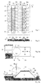
- Figure 1 shows an arrangement according to the invention of Laser diodes, especially pump laser diodes under supervision, Figure 2 in cross section.
- the for dissipating the heat loss from a material good thermal conductivity are laser diodes 2 in up to four rows R1 to R4 side by side arranged. They sit for electrical contacting Laser diodes with their lower connection side on one each Contact area 3, which is larger than the base area of a Laser diode and isolated from the carrier substrate 1 if this consists of an electrically conductive Material exists.
- the laser diodes 2 can in this way can be electrically connected in series.
- the one behind the other switching of the laser diodes takes place via Bond connections 4 from the upper contact side 5 one each laser diode to the contact surface 3, on which the adjacent laser diode is mounted.
- the connections of the Laser diodes at the ends of each row are turned on Pads 6 out on which the power supply from the external wiring (not here drawn).
- a parallel connection of all laser diodes 2 of a row is possible if there are corresponding conductor tracks for the power supply for the upper contact surfaces the carrier substrate 1 can be provided (not shown here).
- the carrier substrate 1 can be the bottom of a Housing (not shown in Figures 1 and 2) for the hermetically sealed enclosure of the overall arrangement of the Pump laser diodes so that they protect against environmental influences are protected and thus their lifespan and Reliability is increased.
- Carrier substrate 1 also on the bottom of such a housing be soldered on. In both cases, the heat loss with low thermal resistance on one under the case bottom large heat sinks are removed and thus an impermissible increase in temperature of the Pump laser diodes can be avoided.
- Exemplary embodiments are seven laser diodes in four Rows R1 to R4 arranged.
- the R1 laser diodes and R2 and the rows R3 and R4 each radiate against each other.
- a prismatic mirror body 7 or 8 Between rows R1 and R2 as well between R3 and R4 is a prismatic mirror body 7 or 8 attached, the side surfaces are mirrored and opposite a flat side of the Carrier substrates 1 have an inclination of 45 °. That on these mirror surfaces 71, 72, 81 and 82 laterally incident light of the laser diode rows R1, R2, R3 and R4 is distracted upwards.
- the mirror surface has to reach under the bottom of the laser diode chip.
- the laser diodes can be soldered onto an intermediate carrier be mounted on the carrier substrate 1 (here not shown), or the prismatic mirror body 7 and 8 are mounted in recesses 11 and 12.
- the Mirror body 7, 8 can then by a known anodic bonding process connected to the carrier substrate 1 become.
- Structuring the depressions 11 and 12 for example Stamping, eroding or milling
- fastening the Mirror body e.g. gluing or soldering
- the Cylinder lenses for each of the four laser rows are placed in the V-shaped gap between the side walls of recesses 11 and 12 and oblique mirror surfaces 71, 72, 81, 82 each side of the prismatic mirror bodies 7 and 8 inserted and fixed without adjustment.
- shape and position of a Cylindrical lens can also take special shots for the Cylinder lenses in the carrier substrate 1 by known Processes such as anisotropic etching can be produced.
- the cylindrical lens 9 is in its focal length and aperture dimensioned so that the transformed beam is a each laser diode in the vertical direction almost the same Divergence as obtained in the horizontal direction.
- the through the common cylindrical lens almost circularly symmetrical transformed and only slightly divergent laser beam hits one of the mirror surfaces 71, 72, 81 or 82 and is redirected upwards.
- On the flat top 73 or 83 of the prismatic mirror body 7 or 8 is for each laser beam a lens holder 13 with a spherical lens 14.
- the lens holder 13 lies with its flat part on the top 73 or 83, and the part of the lens holder that holds the lens 14 protrudes with it over the side surface 71, 72, 81, 82 into the laser beam (see detailed sketch in FIGS. 3a and 3b in cross section or in supervision).
- Out Space reasons can, as shown in Fig.
- each alternately one lens holder to the left and one Lens holder should be facing right when the Corresponding laser diode chips in adjacent rows are staggered.
- a Lens holder 13 on the prismatic mirror body 7 or 8 is the flat top 73 or 83 with a Metallization layer 84 and a solder layer 85 Mistake.
- the bottom of the lens holder in the Area of the support zone with a solder wettable layer 15 provided, the solder layer also on the Lens holder can be applied.
- the distance of the lens 14 from the associated laser diode 2 and the focal length of the lens 14 are selected such that an enlarged image of the laser near field is formed at a distance b from the lens 14 (cf. FIG. 4).
- the end face of an optical fiber 20, in particular a step profile fiber with a core radius r k, is attached in the plane at a distance b in the direction of radiation behind the lens 14.
- the dimension of the radiation source in the plane perpendicular to this is imaged by the cylindrical lens 9 and the lens 10 with the magnification ratio V s in the same image plane at a distance b from the lens 14.
- the magnifications V p and V s are chosen such that the semiaxes of the image of the laser beam waist at a distance b from the lens 14 are smaller than the radius r k of the fiber 20.
- all of the light from a laser diode 2 can enter the Fiber 20 are directed. So that the light can also be guided in the fiber, the maximum incidence angle ⁇ max must not be greater than the acceptance angle ⁇ of the fiber 20.
- the maximum incidence angle ⁇ max results from the image width b and the maximum extent of the laser arrangement on the carrier 1.
- each lens 14 By laterally shifting each lens 14 relative to each associated laser diode 2, the beam can be deflected by a small angle ⁇ x (FIG. 3b) and ⁇ y in the x and y directions (FIG. 3a).
- the beam of each individual pump laser diode can thus be directed into the core of the fiber 20.
- the lenses 14 can be individually adjusted one after the other by all the pump laser diodes of the arrangement according to the invention.
- the lens carrier 13 is preferably laterally displaced by an automatic adjustment system on the top 73 or 83 of the mirror carrier 7 or 8, while the light output coupled into the fiber 20 is measured.
- the laser diode, the radiation of which is being adjusted, is contacted individually with contact needles on the adjacent contact surfaces 3.
- a CCD camera without a lens with a beam diagnosis system can also be attached to its position when carrying out the adjustment.
- Such a system is able to determine the position of the center of gravity of the light distribution on the camera chip. The position coordinates can then be used directly to control the lens shift, so that the adjustment process can be carried out without a complex search process.
- Figure 5 shows the arrangement according to the invention in one common hermetically sealed housing 30 with Fiber connection.
- the fiber 20 is in a flange 21 with a flat flange surface 22.
- the housing is on a side surface 31 also a flat flange surface 32. That consisting of all individual rays Total light beam 33 is shown in FIG Embodiment deflected by a mirror 34 by 90 °.
- This has the advantage that the fiber 20 is parallel to the Base of the carrier substrate 1 can be performed and thus the overall arrangement takes up less space.
- the hermetically sealed closure of the housing 30 is on the Light exit point in the wall 31 through a window 35 reached.
- the transmitted light can be as Monitor signal for the entirety of all pump laser diodes be used. In the exemplary embodiment according to FIG. 5 it is redirected for this purpose and onto a monitor diode 36 directed. Below the carrier substrate 1 is under the Housing bottom to dissipate the heat loss a heat sink 37 attached.
- the position of the mirror 34 and the laser assembly will chosen so that the focus of the total light beam 33 straight into the flange plane of the flange surfaces 32 and 22 and thus falls into the end face of the fiber 20. Assembly tolerances of the mirror 34 can then be reduced the total light signal when all pump laser diodes are in operation by an active lateral adjustment of the flange 21 in the Level up 32. That coupled into the fiber 20 Light can now be coupled to the pump light coupling point pumping solid-state laser.
Landscapes
- Physics & Mathematics (AREA)
- Condensed Matter Physics & Semiconductors (AREA)
- General Physics & Mathematics (AREA)
- Electromagnetism (AREA)
- Optics & Photonics (AREA)
- Optical Couplings Of Light Guides (AREA)
- Semiconductor Lasers (AREA)
Applications Claiming Priority (2)
| Application Number | Priority Date | Filing Date | Title |
|---|---|---|---|
| DE19838518 | 1998-08-25 | ||
| DE19838518A DE19838518A1 (de) | 1998-08-25 | 1998-08-25 | Anordnung |
Publications (2)
| Publication Number | Publication Date |
|---|---|
| EP0982818A2 true EP0982818A2 (fr) | 2000-03-01 |
| EP0982818A3 EP0982818A3 (fr) | 2002-10-02 |
Family
ID=7878607
Family Applications (1)
| Application Number | Title | Priority Date | Filing Date |
|---|---|---|---|
| EP99113961A Withdrawn EP0982818A3 (fr) | 1998-08-25 | 1999-07-17 | Ensemble laser |
Country Status (3)
| Country | Link |
|---|---|
| US (1) | US6501781B1 (fr) |
| EP (1) | EP0982818A3 (fr) |
| DE (1) | DE19838518A1 (fr) |
Cited By (3)
| Publication number | Priority date | Publication date | Assignee | Title |
|---|---|---|---|---|
| WO2000077893A3 (fr) * | 1999-06-11 | 2001-08-02 | Daniel Kopf | Dispositifs laser a pompage par diode presentant une haute puissance et une haute saturation du gain, et dispositif de pompage a reseau de diodes |
| WO2003058720A1 (fr) * | 2002-01-09 | 2003-07-17 | Infineon Technologies Ag | Ensemble photodiode et procede pour la production d'une liaison entre un premier composant semi-conducteur et un deuxieme composant semi-conducteur |
| US7046711B2 (en) | 1999-06-11 | 2006-05-16 | High Q Laser Production Gmbh | High power and high gain saturation diode pumped laser means and diode array pumping device |
Families Citing this family (15)
| Publication number | Priority date | Publication date | Assignee | Title |
|---|---|---|---|---|
| US7331676B2 (en) * | 2005-02-09 | 2008-02-19 | Coherent, Inc. | Apparatus for projecting a reduced image of a photomask using a schwarzschild objective |
| JP5145673B2 (ja) * | 2006-08-30 | 2013-02-20 | 住友電気工業株式会社 | レーザ加工方法およびレーザ加工装置 |
| US7941053B2 (en) * | 2006-10-19 | 2011-05-10 | Emcore Corporation | Optical transceiver for 40 gigabit/second transmission |
| DE102012205513B4 (de) | 2012-04-04 | 2021-12-09 | Osram Gmbh | Verfahren zum Herstellen einer Strahlungsanordnung und Strahlungsanordnung |
| DE102012103257B4 (de) * | 2012-04-16 | 2026-01-29 | OSRAM Opto Semiconductors Gesellschaft mit beschränkter Haftung | Laserdiodenvorrichtung |
| US8897327B2 (en) | 2012-04-16 | 2014-11-25 | Osram Opto Semiconductors Gmbh | Laser diode devices |
| DE102012215487B4 (de) * | 2012-08-31 | 2017-03-23 | Continental Automotive Gmbh | Zündeinrichtung für eine Brennkammer einer Brennkraftmaschine |
| JP6200642B2 (ja) * | 2012-11-30 | 2017-09-20 | 日本オクラロ株式会社 | 光学装置 |
| DE102013104728A1 (de) | 2013-05-07 | 2014-11-13 | Osram Opto Semiconductors Gmbh | Laserdiodenvorrichtung |
| JP6267773B1 (ja) * | 2016-11-16 | 2018-01-24 | 株式会社フジクラ | レーザモジュール |
| CN111758169B (zh) * | 2018-08-03 | 2024-05-14 | 深圳市大疆创新科技有限公司 | 激光二极管封装模块及距离探测装置、电子设备 |
| WO2020133381A1 (fr) * | 2018-12-29 | 2020-07-02 | 泉州三安半导体科技有限公司 | Structure de boîtier laser |
| DE102019110189A1 (de) * | 2019-04-17 | 2020-10-22 | OSRAM Opto Semiconductors Gesellschaft mit beschränkter Haftung | Halbleiterlaser und materialbearbeitungsverfahren mit einem halbleiterlaser |
| CN112636160B (zh) * | 2019-09-20 | 2022-04-26 | 青岛海信激光显示股份有限公司 | 激光器 |
| CN114637161A (zh) * | 2022-03-31 | 2022-06-17 | 青岛海信激光显示股份有限公司 | 一种激光器和激光投影设备 |
Family Cites Families (16)
| Publication number | Priority date | Publication date | Assignee | Title |
|---|---|---|---|---|
| GB1040792A (en) * | 1964-02-24 | 1966-09-01 | Nat Res Dev | Optical systems for lasers |
| US4156206A (en) * | 1976-12-30 | 1979-05-22 | International Business Machines Corporation | Grating coupled waveguide laser apparatus |
| FR2426347A1 (fr) * | 1978-05-18 | 1979-12-14 | Thomson Csf | Source laser a semi-conducteur et son procede de fabrication |
| US4807238A (en) * | 1986-03-12 | 1989-02-21 | Ricoh Co., Ltd. | A semiconductor laser device |
| JPH07123175B2 (ja) * | 1986-09-17 | 1995-12-25 | 株式会社リコー | 半導体レ−ザ装置 |
| US4881237A (en) * | 1988-08-26 | 1989-11-14 | Massachusetts Institute Of Technology | Hybrid two-dimensional surface-emitting laser arrays |
| FR2639150B1 (fr) * | 1988-11-15 | 1991-01-25 | Thomson Hybrides Microondes | Dispositif optoelectronique de puissance et son procede de realisation |
| US4956844A (en) * | 1989-03-17 | 1990-09-11 | Massachusetts Institute Of Technology | Two-dimensional surface-emitting laser array |
| DE3914835C1 (fr) * | 1989-05-05 | 1990-07-26 | Ant Nachrichtentechnik Gmbh, 7150 Backnang, De | |
| US5168401A (en) * | 1991-05-07 | 1992-12-01 | Spectra Diode Laboratories, Inc. | Brightness conserving optical system for modifying beam symmetry |
| FR2684811B1 (fr) * | 1991-12-10 | 1994-01-28 | Thomson Hybrides | Systeme d'alimentation electrique d'un circuit integre de lasers semiconducteurs. |
| US5268978A (en) * | 1992-12-18 | 1993-12-07 | Polaroid Corporation | Optical fiber laser and geometric coupler |
| DE59305898D1 (de) * | 1993-12-22 | 1997-04-24 | Siemens Ag | Optoelektronisches Bauelement und Verfahren zu dessen Herstellung |
| US5557475A (en) | 1994-07-12 | 1996-09-17 | Coherent, Inc. | Optical system for improving the symmetry of the beam emitted from a broad area laser diode |
| US5793792A (en) * | 1996-05-08 | 1998-08-11 | Polaroid Corporation | Laser assembly with integral beam-shaping lens |
| DE19704502C1 (de) * | 1997-02-06 | 1998-02-26 | Siemens Ag | Lasermodul mit Ankoppeloptik und Verfahren zur Feinjustierung der Ankoppeloptik |
-
1998
- 1998-08-25 DE DE19838518A patent/DE19838518A1/de not_active Withdrawn
-
1999
- 1999-07-17 EP EP99113961A patent/EP0982818A3/fr not_active Withdrawn
- 1999-08-11 US US09/372,303 patent/US6501781B1/en not_active Expired - Fee Related
Cited By (4)
| Publication number | Priority date | Publication date | Assignee | Title |
|---|---|---|---|---|
| WO2000077893A3 (fr) * | 1999-06-11 | 2001-08-02 | Daniel Kopf | Dispositifs laser a pompage par diode presentant une haute puissance et une haute saturation du gain, et dispositif de pompage a reseau de diodes |
| US7046711B2 (en) | 1999-06-11 | 2006-05-16 | High Q Laser Production Gmbh | High power and high gain saturation diode pumped laser means and diode array pumping device |
| WO2003058720A1 (fr) * | 2002-01-09 | 2003-07-17 | Infineon Technologies Ag | Ensemble photodiode et procede pour la production d'une liaison entre un premier composant semi-conducteur et un deuxieme composant semi-conducteur |
| US7476906B2 (en) | 2002-01-09 | 2009-01-13 | Osram Opto Semiconductors Gmbh | Photodiode array and method for establishing a link between a first semiconductor element and a second semiconductor element |
Also Published As
| Publication number | Publication date |
|---|---|
| EP0982818A3 (fr) | 2002-10-02 |
| DE19838518A1 (de) | 2000-03-02 |
| US6501781B1 (en) | 2002-12-31 |
Similar Documents
| Publication | Publication Date | Title |
|---|---|---|
| EP0982818A2 (fr) | Ensemble laser | |
| DE69736133T2 (de) | Direktes hochleistungslaserdiodensystem mit hoher effizienz und zugehörende verfahren | |
| DE102004045912B4 (de) | Verfahren und Vorrichtung zur Überlagerung von Strahlenbündeln | |
| EP2976817B1 (fr) | Ensemble laser | |
| WO2020212221A1 (fr) | Laser à semi-conducteurs et procédé d'usinage de matériau avec un laser à semi-conducteurs | |
| EP0423513A2 (fr) | Procédé de fabrication d'une plaquette à laser | |
| DE19723269A1 (de) | Festkörperlaser mit einer oder mehreren Pumplichtquellen | |
| EP1071178B1 (fr) | Laser à l'état solide à modes synchrones | |
| DE69204135T2 (de) | Breiter Diodenstreifenlaser mit Linse. | |
| DE102022115367A1 (de) | Halbleiterlaservorrichtung | |
| EP3577514B1 (fr) | Procédé pour la collimation d'un rayonnement lumineux, laser haute puissance et optique de focalisation et procédé de collimation d'un rayonnement lumineux | |
| DE4101403C2 (de) | Halbleiterlaser-gepumpter Festkörperlaser | |
| DE19927054A1 (de) | Festkörperlaser | |
| DE19841040A1 (de) | Vorrichtung zum Markieren einer Oberfläche mittels Laserstrahlen | |
| DE69924544T2 (de) | Faserlaser | |
| DE10204246A1 (de) | Festkörper-Laserverstärkersystem | |
| DE4008225C2 (de) | Laserdiodengepumpter Festkörperlaser | |
| DE19803728B4 (de) | Halbleiteranregungs-Festkörperlaservorrichtung | |
| WO2004021524A2 (fr) | Dispositif laser a semiconducteurs | |
| DE102004045914B4 (de) | Verfahren und Vorrichtung zur Überlagerung von Strahlenbündeln | |
| EP2976816B1 (fr) | Ensemble laser | |
| EP1252541A2 (fr) | Procede de realisation d'un module d'emission optique | |
| DE19925648B4 (de) | Lasersystem mit einer Hohlspiegelanordnung | |
| DE4207824C2 (de) | Laserkristall für einen Festkörperlaser oder -verstärker | |
| DE10240949A1 (de) | Halbleiterlaservorrichtung |
Legal Events
| Date | Code | Title | Description |
|---|---|---|---|
| PUAI | Public reference made under article 153(3) epc to a published international application that has entered the european phase |
Free format text: ORIGINAL CODE: 0009012 |
|
| AK | Designated contracting states |
Kind code of ref document: A2 Designated state(s): AT BE CH CY DE DK ES FI FR GB GR IE IT LI LU MC NL PT SE |
|
| AX | Request for extension of the european patent |
Free format text: AL;LT;LV;MK;RO;SI |
|
| PUAL | Search report despatched |
Free format text: ORIGINAL CODE: 0009013 |
|
| AK | Designated contracting states |
Kind code of ref document: A3 Designated state(s): AT BE CH CY DE DK ES FI FR GB GR IE IT LI LU MC NL PT SE |
|
| AX | Request for extension of the european patent |
Free format text: AL;LT;LV;MK;RO;SI |
|
| RIC1 | Information provided on ipc code assigned before grant |
Free format text: 7H 01S 3/0941 A, 7H 01S 5/40 B, 7G 02B 6/42 B |
|
| 17P | Request for examination filed |
Effective date: 20030402 |
|
| 17Q | First examination report despatched |
Effective date: 20030513 |
|
| AKX | Designation fees paid |
Designated state(s): DE FR GB IT NL SE |
|
| RAP1 | Party data changed (applicant data changed or rights of an application transferred) |
Owner name: MARCONI COMMUNICATIONS GMBH |
|
| RAP1 | Party data changed (applicant data changed or rights of an application transferred) |
Owner name: MARCONI UK INTELLECTUAL PROPERTY LTD |
|
| GRAP | Despatch of communication of intention to grant a patent |
Free format text: ORIGINAL CODE: EPIDOSNIGR1 |
|
| STAA | Information on the status of an ep patent application or granted ep patent |
Free format text: STATUS: THE APPLICATION IS DEEMED TO BE WITHDRAWN |
|
| 18D | Application deemed to be withdrawn |
Effective date: 20040817 |