EP0982841A2 - Pulsweitenmodulierter Gleichspannungswandler - Google Patents
Pulsweitenmodulierter Gleichspannungswandler Download PDFInfo
- Publication number
- EP0982841A2 EP0982841A2 EP99115994A EP99115994A EP0982841A2 EP 0982841 A2 EP0982841 A2 EP 0982841A2 EP 99115994 A EP99115994 A EP 99115994A EP 99115994 A EP99115994 A EP 99115994A EP 0982841 A2 EP0982841 A2 EP 0982841A2
- Authority
- EP
- European Patent Office
- Prior art keywords
- voltage
- transistor
- current
- converter according
- choke
- Prior art date
- Legal status (The legal status is an assumption and is not a legal conclusion. Google has not performed a legal analysis and makes no representation as to the accuracy of the status listed.)
- Withdrawn
Links
- 239000003990 capacitor Substances 0.000 claims description 13
- 238000009499 grossing Methods 0.000 claims description 7
- 230000010354 integration Effects 0.000 claims 1
- 230000006978 adaptation Effects 0.000 description 2
- 230000003321 amplification Effects 0.000 description 2
- 238000003199 nucleic acid amplification method Methods 0.000 description 2
- 230000004913 activation Effects 0.000 description 1
- 230000002411 adverse Effects 0.000 description 1
- 230000000694 effects Effects 0.000 description 1
- 230000002349 favourable effect Effects 0.000 description 1
- 238000000034 method Methods 0.000 description 1
- 230000001105 regulatory effect Effects 0.000 description 1
Images


Classifications
-
- G—PHYSICS
- G05—CONTROLLING; REGULATING
- G05F—SYSTEMS FOR REGULATING ELECTRIC OR MAGNETIC VARIABLES
- G05F1/00—Automatic systems in which deviations of an electric quantity from one or more predetermined values are detected at the output of the system and fed back to a device within the system to restore the detected quantity to its predetermined value or values, i.e. retroactive systems
- G05F1/10—Regulating voltage or current
- G05F1/46—Regulating voltage or current wherein the variable actually regulated by the final control device is DC
- G05F1/613—Regulating voltage or current wherein the variable actually regulated by the final control device is DC using semiconductor devices in parallel with the load as final control devices
Definitions
- the invention relates to a pulse width modulated direct voltage converter a series circuit of a switching transistor and a choke inductance, wherein parallel to the switching transistor a smoothing capacitance and a switching element in Series are connected so that one at the series circuit from the switching transistor and the choke inductance input voltage in a larger, at the Smoothing capacity tapped output voltage is converted with a Error amplifier, the first input of which is connected to a voltage divider Output voltage can be supplied, and its second input with a Reference voltage source is connected, and with a comparator, the first Input with the output of the error amplifier, the second input with a by means of a signal proportional to the choke current of the choke inductance compensated ramp generator and its output with the gate electrode of the Switching transistor is connected.
- Such a DC-DC converter is from MAXIM data sheet: MAX 731 / MAX 752, 19-4672; REV 2; 2/93 known.
- the output voltage is fed back via the voltage divider Error amplifier and the comparator with the ramp voltage of the Ramp generator compared and led to the switching transistor to there Set the duty cycle for the constant output voltage.
- a flip-flop connected to the clock frequency a time control circuit (clock) for the precise, clocked activation of the Switching transistor is supplied.
- the stability limit of the feedback DC-DC converter is a function of the choke current through the choke inductance and the inverse of the Input voltage.
- the inductor current is a function of the load current and the Input voltage.
- the amount of loop gain is determined by the choke current and affects the inverse of the input voltage. With increasing choke current increases the amount of loop gain whereas the system's poles, i.e. the Phase rotations of the loop gain remain unchanged. This leads to a Reduction of the phase reserve and thus instability of the system.
- capacitors are parallel to the voltage divider switched, which influence the frequency response so that for a certain Range of load currents and of the input voltage sufficient stability is achieved. Since the pole points by the smoothing capacity and the Choke inductance can be determined at very low frequencies are considered Compensation capacities require very large capacities. These are with one monolithically integrated circuit cannot be integrated into the system.
- Another measure to stabilize the DC-DC converter exists in that to the ramp voltage of the ramp generator by means of a Adding amplifier a voltage is added, which is proportional to the inductor current. A voltage is used which is proportional to the current through the Switching transistor is. The comparator switches at high inductor currents earlier, so the turn-on time of the switching transistor and the amount of Loop gain can be reduced.
- This compensation has the disadvantage that an additional, precise adder amplifier to compensate for the ramp generator is needed.
- Another disadvantage is that the amount of loop gain at high choke current is reduced at the beginning of the switch-on cycle. This reduces the gain even at high input voltages, which adversely affects the accuracy of the output voltage.
- the invention has for its object an improved pulse width modulated To create DC converters.
- a generic DC converter in which the compensated ramp generator is designed so that the Choke current of the inductance proportional signal of the ramp-shaped Voltage can be superimposed in such a way that an output voltage is generated which a sawtooth curve with a concave increase in voltage having.
- Ramp generator designed so that the sum of a correction current, which is proportional to the inductor current, and a constant reference current in the Ramp generator can be integrated so that the output voltage of the Ramp generator has a quadratic voltage increase. This will a frequency response of the DC converter achieved in a simple manner. It doesn't have to be elaborate Large area device such as an accurate adder amplifier be used.
- the sum is integrated from the correction current and the constant reference current in that the Correction current and the constant reference current can be supplied to a capacitor, which via a parallel switching element with the frequency of the gate electrode of the switching transistor supplied signal can be discharged. This will turn on easily generates a quadratic voltage rise in the ramp voltage.
- a first amplifier can advantageously be used to generate the correction current be provided, the input of which is a voltage proportional to the inductor current can be fed, and its output via a resistor with a first Node of constant potential is connected to which the correction current is feedable.
- a buffer whose gain is equal to one can be used as an amplifier be used. This can be done by a feedback operational amplifier will be realized.
- the operational amplifier can be designed so that its Output stage a first reference current source with a first transistor in Source circuit is connected in series.
- A can be used to generate the constant node potential in the first node second operational amplifier can be provided.
- the first entrance of the second Operational amplifier is with a first constant reference voltage source, the second input of the operational amplifier is connected to the first node.
- the first node provides the constant node potential with low resistance and is connected to the output of the second operational amplifier.
- the second Operational amplifiers can be designed so that its output stage is a second Reference current source connected in series with a second transistor in source circuit is switched, includes. In the node, the sum of the Correction current and the constant reference current flow.
- a current mirror can be used be provided, the sum of the correction current generated at the node and maps the constant reference current to the capacitor.
- the current mirror can consist of the first or the second operational amplifier and a third Transistor are formed in the source circuit.
- the gate electrode of the third Transistor is with the gate electrode of the first transistor and the drain electrode of the third transistor connected to the capacitor.
- the exemplary embodiment is the gate electrode of the third transistor with the gate electrode of the second transistor and the drain electrode of the third transistor a second current mirror connected to the capacitor.
- the first transistor and the second transistor can have a fixed ratio in terms of their electrical properties. For MOS-FET transistors this is determined by a fixed ratio of the W / L (longitude / latitude) ratio of the transistors reached.
- the first and the second Reference current source currents that have a fixed relationship to each other be generated. When the reference current sources generate equal currents and the first and the second transistor have the same electrical properties Circuit equal conditions before, so that a good adaptation, i.e. a good Matching, which exists individual circuit elements, whereby electrical influences, Influences due to temperature or mask alignment errors can be avoided.
- the signal proportional to the inductor current can be derived from the voltage drop across the Switching transistor can be determined. This is possible because the switching transistor in Triode region is operated so that it has a resistance behavior. Methods for determining the inductor current are from the prior art, known for example from P 198 12299.3. The arrangement is advantageous integrated monolithically.
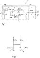
- the DC-DC converter 1 shows a basic arrangement of a pulse-width-modulated DC-DC converter 1 according to the invention.
- the DC-DC converter 1 comprises a series circuit comprising a switching transistor 2 and a choke inductor 3. A smoothing capacitance 4 and a switching element are connected in series with the switching transistor 2.
- V in an input voltage V in at the series circuit comprising the switching transistor 2 and the inductor 3 is converted into a larger output voltage V out which can be tapped at the smoothing capacitance 4.
- the output voltage V out is fed back to the DC-DC converter 1 via a voltage divider 6, which comprises two resistors.
- An error amplifier 7 is provided, the first input of which is connected to the voltage divider 6 and the second input of which is connected to a reference voltage source V ref .
- a comparator 8 is provided, the first input of which is connected to the output of the error amplifier 7, the second input of which is connected to a ramp generator 9 which is compensated for by a signal proportional to the inductor current I inductor 3 and the output of which is connected to the gate electrode of the switching transistor 2 .
- the compensated ramp generator 9 is designed such that it generates an output voltage which has a sawtooth curve shape with a concave voltage rise. This voltage curve is generated by the superimposition of the signal proportional to the choke current of the choke inductor 3 with the ramp-shaped voltage of the ramp generator 9.
- the output of the comparator 8 is connected to the gate of the switching transistor 2 via a flip-flop element 20.
- the flip-flop element 20 is controlled by means of a timing control circuit with a signal of the frequency f clock . It is an RS (reset / set) flip-flop with a reset input R, a set input S and an active output Q, which is connected to the gate of the switching transistor 2.
- the frequency f clock of the signal of the timing control circuit is tuned to the frequency of the signal of the ramp generator 9.
- the frequency for switching the switching transistor 2 is determined by the output signal of the comparator 8.
- the duty cycle of the switching transistor is changed by the output voltage, whereby the output voltage V out is regulated. If the output voltage V out is too high, the output voltage V error of the error amplifier is reduced. This reduces the switching time T E of the switching transistor and thus the output voltage V out of the DC converter.
- a capacitor 10 is provided, to which the sum of the correction current I corr and the constant reference current L ref is supplied.
- a switching element 11 is connected, to which a signal is supplied, which the switching element 11 can be discharged with the frequency of the signal supplied to the gate electrode of the switching transistor 2.
- 3a shows the course of the choke current I choke , to which the correction current I corr is proportional, as a function of time.
- the current profile for a low choke current and 1 the current profile for a high choke current are identified by 1.
- 3b shows the output voltage of the ramp generator V Ramp for the two current profiles 1 and 2 from FIG. 3a. The voltage curve is parabolic, so that the zero point of the output voltage of the ramp generator V Ramp is maintained.
- the output voltage V Error of the error amplifier as a function of time is also shown.
- the intersection of V Error with V Ramp is determined with the comparator 8.
- the clock frequency with which the switching transistor 2 is driven is determined by these intersections.
- a higher choke current leads to a lower switch-on time T E.
- the switch-on time T E of the ramp generator compensated according to the invention is shorter than the switch-on time T E of the non-compensated ramp generator for all, ie also for lower choke currents.
- the slew rate (rate of voltage rise) of the output voltage of the compensated ramp generator 9 increases with large choke currents (2).
- the choke current increases both with an increase in the output current and with a constant output current and a decrease in the input voltage.
- the amount of loop gain of the feedback DC-DC converter 1 is only reduced when the inductor currents are high and the input voltages are lower.
- the frequency response of the overall system can be kept constant over a very large range, regardless of the input voltage and the load current. A smaller amount of loop gain at high input voltages and thus a loss in the accuracy of the DC-DC converter is thus avoided.
- the correction current I corr is generated in a first node K1 of constant potential.
- a first amplifier 12 is provided, the input of which is supplied with a voltage V D proportional to the inductor current I inductor .
- the output of the first amplifier 12 is connected to the first node K1 via a resistor 13.
- the first amplifier 12 is a feedback operational amplifier and may have a gain that is equal to 1.
- a first reference current source 14 and a first transistor 15 connected in series therewith are provided in source circuit, which form an output stage of the amplifier 12.
- the output of a second operational amplifier 17 is connected to the node K1.
- One input of the second operational amplifier 17 is connected to a second reference voltage source V ref1 , and the other input of the second operational amplifier 17 is connected to the node K1.
- the output stage of the second operational amplifier 17 is formed by the series connection of the second transistor 18 and a second reference current source 16. At the node K1, the sum of the correction current I corr and the constant reference current I ref is formed.
- a third transistor 19 forms a current mirror with the first operational amplifier 12 and its output stage, which consists of the first reference current source 14 and the first transistor 15.
- the gate electrode of the third transistor 19 is connected to the gate electrode of the first transistor 15, the drain electrode of the third transistor 19 to the capacitor 10.
- the first transistor 15 and the second transistor 18 have a fixed ratio with regard to their electrical properties to each other.
- the first and the second reference current sources 14, 16 generate currents which have a fixed relationship to one another.
- the first transistor 15 and the second transistor 18 can also have the same electrical properties and the first and the second reference current sources 14, 16 can generate the same currents. In this case, a particularly good adaptation of the overall system is achieved. Errors due to different adjustments are avoided.
- the entire arrangement can be integrated monolithically.
- the signal proportional to the choke current I choke can be determined from the voltage drop across the switching transistor 2.
- FIG. 5 shows an exemplary embodiment of the compensated ramp generator, in which the elements that have the same reference numerals correspond to those from FIG. 4.
- the gate electrode of the third transistor 19 is connected to the gate electrode of the second transistor 18.
- the drain electrode of the third transistor 19 is connected to the capacitor 10 via a second current mirror 21.
- n-channel MOS transistors are used, whereas in the embodiment shown in FIG. 4, p-channel MOS transistors are used.
- the second current mirror 21 reverses the potential relationships. Accordingly, in the exemplary embodiment of FIG. 5, the connections of the circuit elements to the reference voltage V ref and to the input voltage V D are interchanged in comparison with that of FIG. 4, so that the circuit in the two exemplary embodiments takes into account the second current mirror 21 in the Fig. 5 get the same sense of control.
Landscapes
- Engineering & Computer Science (AREA)
- Physics & Mathematics (AREA)
- Electromagnetism (AREA)
- General Physics & Mathematics (AREA)
- Radar, Positioning & Navigation (AREA)
- Automation & Control Theory (AREA)
- Dc-Dc Converters (AREA)
Abstract
Description
Claims (15)
- Pulsweitenmodulierter Gleichspannungswandler mit einer Reihenschaltung aus einem Schalttransistor (2) und einer Drosselinduktivität (3), wobei parallel zu dem Schalttransistor (3) eine Glättungskapazität (4) und ein Schaltelement (5) in Reihe geschaltet sind, so daß eine an der Reihenschaltung aus dem Schalttransistor (2) und der Drosselinduktivität (3) liegende Eingangsspannung (Vin) in eine größere, an der Glättungskapazität (4) abgreifbare Ausgangsspannung (Vout) umgewandelt wird, mit einem Fehlerverstärker (7), dessen erster Eingang mit einem Spannungsteiler (6), dem die Ausgangsspannung zuführbar ist, und dessen zweiter Eingang mit einer Referenzspannungsquelle (Vref) verbunden ist, mit einem Komparator (8), dessen erster Eingang mit dem Ausgang des Fehlerverstärkers (7), dessen zweiter Eingang mit einem mittels eines zu dem Drosselstrom (IDrossel) der Drosselinduktivität proportionalen Signal kompensierten Rampengenerator (9) und dessen Ausgang mit der Gate-Elektrode des Schalttransistors (2) verbunden ist, dadurch gekennzeichnet, daß der kompensierte Rampengenerator (9) so ausgebildet ist, daß das dem Drosselstrom (IDrossel) der Drosselinduktivität (3) proportionale Signal der rampenförmigen Spannung derart überlagerbar ist, daß eine Ausgangsspannung erzeugbar ist, die einen sägezahnförmigen Kurvenverlauf mit einem konkaven Spannungsanstieg aufweist.
- Gleichspannungswandler nach Anspruch 1, dadurch gekennzeichnet daß der Rampengenerator (9) so ausgebildet ist, daß die Summe aus einem Korrekturstrom (Icorr), welcher proportional zu dem Drosselstrom (IDrossel) ist, und einem konstanten Referenzstrom (Iref) in dem Rampengenerator (9) integrierbar ist, so daß die Ausgangsspannung (VRamp) des Rampengenerators (9) einen quadratischen Spannungsanstieg aufweist.
- Gleichspannungswandler nach Anspruch 2, dadurch gekennzeichnet, daß die Integration der Summe aus dem Korrekturstrom (Icorr) und dem konstanten Referenzstrom (Iref) dadurch erfolgt, daß der Korrekturstrom (Icorr) und der konstante Referenzstrom (Iref) einem Kondensator (10) zuführbar sind, welcher über ein parallelgeschaltetes Schaltelement (11) mit der Frequenz des der Gateelektrode des Schalttransistors (2) zugeführten Signals entladbar ist.
- Gleichspannungswandler nach einem der vorangehenden Ansprüche, dadurch gekennzeichnet, daß zur Erzeugung des Korrekturstromes (Icorr) ein erster Verstärker (12) vorgesehen ist, dessen Eingang eine dem Drosselstrom (IDrossel) proportionale Spannung (VD) zuführbar ist, und dessen Ausgang über einen Widerstand (13) mit einem ersten Knotenpunkt (K1) von konstantem Potential verbunden ist, welchem der Korrekturstrom (Icorr) zuführbar ist.
- Gleichspannungswandler nach Anspruch 4, dadurch gekennzeichnet, daß als Verstärker (12) ein Buffer, dessen Verstärkung gleich eins ist, verwendet wird.
- Gleichspannungswandler nach Anspruch 4 oder 5, dadurch gekennzeichnet, daß als Verstärker (12) ein rückgekoppelter Operationsverstärker vorgesehen ist.
- Gleichspannungswandler nach Anspruch 6, dadurch gekennzeichnet, daß eine Ausgangsstufe des Operationsverstärkers eine erste Referenzstromquelle (14), die mit einem ersten Transitor (15) in Source-Schaltung in Reihe geschaltet ist, umfaßt.
- Gleichspannungswandler nach einem der vorangehenden Ansprüche, dadurch gekennzeichnet, daß das konstante Knotenpotential in dem Knotenpunkt K1 durch einen zweiten Operationsverstärker (17) und eine Referenzspannungsquelle Vref1 erzeugt wird.
- Gleichspannungswandler nach Anspruch 8, dadurch gekennzeichnet, daß der zweite Operationsverstärker (17) eine Ausgangsstufe mit einer Reihenschaltung aus einer Stromquelle (16) und einem zweiten Transistor 18 in Source-Schaltung umfaßt.
- Gleichspannungswandler nach einem der Ansprüche 4 bis 9, dadurch gekennzeichnet, daß ein dritter Transistor (19) vorgesehen ist, dessen Gate-Elektrode mit der Gate-Elektrode des ersten Transistors (15) verbunden ist, wobei der erste Transistor (15) und der dritte Transistor (19) zusammen mit dem ersten Verstärker (12) einen Stromspiegel bilden, dessen Ausgang an den Kondensator (10) angeschlossen ist.
- Gleichspannungswandler nach einem der Ansprüche 4 bis 9, dadurch gekennzeichnet, daß die Gate-Elektrode des dritten Transistors (19) mit der Gate-Elektrode des zweiten Transistors (18) verbunden ist, der zweite Transistor (18) und der dritte Transistor (19) zusammen mit dem zweiten Operationsverstärker (17) einen Stromspiegel bilden, dessen Ausgang über einen zweiten Stromspiegel (21) an den Kondensator (10) angeschlossen ist.
- Gleichspannungswandler nach Anspruch 10 oder 11, dadurch gekennzeichnet, daß der erste Transistor (15) und der zweite Transistor (18) ein festes Verhältnis hinsichtlich ihrer elektrischen Eigenschaften zueinander haben.
- Gleichspannungswandler nach einem der Ansprüche 10 bis 12, dadurch gekennzeichnet daß mit der ersten und der zweiten Referenzstromquelle (16, 14) Ströme, die ein festes Verhältnis zueinander haben, erzeugbar sind.
- Gleichspannungswandler nach einem der vorangehenden Ansprüche, dadurch gekennzeichnet daß das dem Drosselstrom (IDrossel) proportionale Signal VD aus dem Spannungsabfall an dem Schalttransistor (2) bestimmt wird.
- Gleichspannungswandler nach einem der vorangehenden Ansprüche, dadurch gekennzeichnet daß die Anordnung monolithisch integriert ist.
Applications Claiming Priority (2)
| Application Number | Priority Date | Filing Date | Title |
|---|---|---|---|
| DE19837153 | 1998-08-17 | ||
| DE19837153A DE19837153A1 (de) | 1998-08-17 | 1998-08-17 | Pulsweitenmodulierter Gleichspannungswandler |
Publications (2)
| Publication Number | Publication Date |
|---|---|
| EP0982841A2 true EP0982841A2 (de) | 2000-03-01 |
| EP0982841A3 EP0982841A3 (de) | 2000-08-09 |
Family
ID=7877717
Family Applications (1)
| Application Number | Title | Priority Date | Filing Date |
|---|---|---|---|
| EP99115994A Withdrawn EP0982841A3 (de) | 1998-08-17 | 1999-08-14 | Pulsweitenmodulierter Gleichspannungswandler |
Country Status (3)
| Country | Link |
|---|---|
| US (1) | US6522115B1 (de) |
| EP (1) | EP0982841A3 (de) |
| DE (1) | DE19837153A1 (de) |
Families Citing this family (32)
| Publication number | Priority date | Publication date | Assignee | Title |
|---|---|---|---|---|
| DE10056293A1 (de) * | 2000-11-14 | 2002-06-06 | Infineon Technologies Ag | Schaltungsanordnung zur Erzeugung einer steuerbaren Ausgangsspannung |
| ATE410815T1 (de) * | 2001-07-05 | 2008-10-15 | Power One Inc | Induktivitätsstrommessung in isolierten schaltreglern und damit zusammenhängende verfahren |
| US6734656B2 (en) * | 2001-12-10 | 2004-05-11 | Intersil Americas Inc. | Buck regulator with monolithic N- channel upper FET and pilot current sensing |
| JP3963257B2 (ja) * | 2002-02-14 | 2007-08-22 | 富士通株式会社 | Dc−dcコンバータ、電子機器、デューティ比設定回路 |
| JP3563066B2 (ja) * | 2002-04-02 | 2004-09-08 | ローム株式会社 | 電源装置及びそれを備えた携帯機器 |
| JP3990359B2 (ja) * | 2002-04-03 | 2007-10-10 | インターナショナル・レクチファイヤー・コーポレーション | 同期バックコンバータ |
| DE10250359A1 (de) | 2002-10-29 | 2004-05-19 | Infineon Technologies Ag | Gleichspannungsschaltregler |
| FR2848359A1 (fr) * | 2002-12-04 | 2004-06-11 | St Microelectronics Sa | Generateur d'impulsions modulees en largeur |
| US6997753B2 (en) * | 2003-10-22 | 2006-02-14 | Gore Enterprise Holdings, Inc. | Apparatus, system and method for improved calibration and measurement of differential devices |
| JP4461842B2 (ja) * | 2004-03-09 | 2010-05-12 | 株式会社デンソー | スイッチングレギュレータ及びスイッチングレギュレータの制御方法 |
| US20050215700A1 (en) * | 2004-03-25 | 2005-09-29 | Faust Hans U | Bicomponent adhesive with improved heat resistance and extended pot life |
| US6912144B1 (en) * | 2004-08-19 | 2005-06-28 | International Rectifier Corporation | Method and apparatus for adjusting current amongst phases of a multi-phase converter |
| KR101219033B1 (ko) * | 2004-08-20 | 2013-01-07 | 삼성디스플레이 주식회사 | 전원 공급 장치 및 표시 장치 |
| US7638995B2 (en) * | 2005-01-18 | 2009-12-29 | Freescale Semiconductor, Inc. | Clocked ramp apparatus for voltage regulator softstart and method for softstarting voltage regulators |
| US7388413B1 (en) | 2005-07-14 | 2008-06-17 | Microsemi Corporation | Ramp generator with fast reset |
| JP2007129841A (ja) * | 2005-11-04 | 2007-05-24 | Toshiba Corp | 電源回路および半導体集積装置 |
| US7489121B2 (en) * | 2005-11-16 | 2009-02-10 | Intersil Americas Inc. | Compensation offset adjustment scheme for fast reference voltage transitioning |
| US7298125B1 (en) * | 2006-04-26 | 2007-11-20 | Micrel, Incorporated | Right half-plane zero compensation and cancellation for switching regulators |
| CN100559686C (zh) * | 2006-09-22 | 2009-11-11 | 立锜科技股份有限公司 | 产生脉冲宽度调制信号的方法与装置、及其应用 |
| RU2323515C1 (ru) * | 2006-10-23 | 2008-04-27 | Новосибирский государственный технический университет | Регулируемый понижающий преобразователь постоянного напряжения |
| US7391242B1 (en) | 2007-04-07 | 2008-06-24 | Ball Newton E | Sawtooth waveform generator |
| US7986154B2 (en) * | 2008-05-02 | 2011-07-26 | Sony Ericsson Mobile Communications Ab | Capacitive sensing slide detection |
| CN103236791B (zh) * | 2008-08-21 | 2016-01-20 | 立锜科技股份有限公司 | 改善动态反应的pwm电源转换器及其控制方法 |
| TWI396954B (zh) * | 2009-11-11 | 2013-05-21 | Richtek Technology Corp | 用於變頻式電壓調節器的頻率控制電路及方法 |
| TWI395082B (zh) * | 2009-11-11 | 2013-05-01 | Richtek Technology Corp | 用於變頻式電壓調節器的頻率控制電路及方法 |
| US8138740B2 (en) * | 2010-01-29 | 2012-03-20 | Iml International | Non-linear compensation ramp for current mode pulse width modulation |
| TWI491149B (zh) * | 2013-05-13 | 2015-07-01 | Upi Semiconductor Corp | 直流轉直流控制器及其多斜坡信號的操作方法 |
| CN104466913B (zh) * | 2014-12-02 | 2017-07-18 | 成都芯源系统有限公司 | 开关变换电路及其方法 |
| CN111900861B (zh) * | 2020-08-13 | 2025-06-13 | 杰华特微电子股份有限公司 | 一种开关电源的控制电路、控制方法及开关电源 |
| US11567520B2 (en) * | 2021-04-07 | 2023-01-31 | Texas Instruments Incorporated | Exponential-based slope compensation |
| CN114995567B (zh) * | 2022-06-20 | 2023-07-07 | 西安微电子技术研究所 | 一种电流控制型的斜率补偿电路 |
| CN117175938B (zh) * | 2023-11-02 | 2024-01-30 | 拓尔微电子股份有限公司 | 一种直流-直流转换器 |
Citations (1)
| Publication number | Priority date | Publication date | Assignee | Title |
|---|---|---|---|---|
| US4546421A (en) * | 1984-03-28 | 1985-10-08 | United Technologies Corporation | Flyback feedforward pulse width modulation regulator |
Family Cites Families (11)
| Publication number | Priority date | Publication date | Assignee | Title |
|---|---|---|---|---|
| US4825347A (en) * | 1987-09-03 | 1989-04-25 | Unisys Corporation | Pulse width modulation control circuit |
| US5003454A (en) * | 1990-01-09 | 1991-03-26 | North American Philips Corporation | Power supply with improved power factor correction |
| JPH03234442A (ja) | 1990-02-06 | 1991-10-18 | Fuji Heavy Ind Ltd | 打鋲方法およびその装置 |
| EP0498553B1 (de) * | 1991-02-05 | 1997-05-28 | Lambda Electronics, Inc. | Adaptivsteuerungsverfahren für Leistungswandler |
| DE9117264U1 (de) * | 1991-04-19 | 1998-10-01 | Deutsche Thomson-Brandt Gmbh, 78048 Villingen-Schwenningen | Schaltnetzteil |
| EP0626669A3 (de) * | 1993-05-26 | 1998-02-18 | International Business Machines Corporation | Ablenkungsschaltung für nach dem Rasterverfahren arbeitende Kathodenstrahlanzeigegeräte |
| US5361048A (en) * | 1993-08-30 | 1994-11-01 | Motorola, Inc. | Pulse width modulator having a duty cycle proportional to the amplitude of an input signal from a differential transducer amplifier |
| JP3234442B2 (ja) | 1995-05-10 | 2001-12-04 | 株式会社さとうベネック | 建築物のビルドアンドスクラップ式構築方法 |
| US5680036A (en) * | 1996-03-19 | 1997-10-21 | Compaq Computer Corporation | Logarithmic power compensation for a switching power supply |
| DE69724094D1 (de) * | 1997-04-09 | 2003-09-18 | St Microelectronics Srl | Steuerung der Ausgangsleistung eines Gleichstromwandlers variabler Schaltfrequenz |
| US5982156A (en) * | 1997-04-15 | 1999-11-09 | The United States Of America As Represented By The Secretary Of The Air Force | Feed-forward control of aircraft bus dc boost converter |
-
1998
- 1998-08-17 DE DE19837153A patent/DE19837153A1/de not_active Ceased
-
1999
- 1999-08-09 US US09/370,271 patent/US6522115B1/en not_active Expired - Lifetime
- 1999-08-14 EP EP99115994A patent/EP0982841A3/de not_active Withdrawn
Patent Citations (1)
| Publication number | Priority date | Publication date | Assignee | Title |
|---|---|---|---|---|
| US4546421A (en) * | 1984-03-28 | 1985-10-08 | United Technologies Corporation | Flyback feedforward pulse width modulation regulator |
Non-Patent Citations (1)
| Title |
|---|
| ALAN B GREBENE: "Part II: Switching regulators", BIPOLAR AND MOS ANALOG INTEGRATED CIRCUIT DESIGN, WILEY, US, 1984, pages 514 - 539, XP009127763, ISBN: 978-0-471-08529-4 * |
Also Published As
| Publication number | Publication date |
|---|---|
| US6522115B1 (en) | 2003-02-18 |
| EP0982841A3 (de) | 2000-08-09 |
| DE19837153A1 (de) | 2000-03-02 |
Similar Documents
| Publication | Publication Date | Title |
|---|---|---|
| DE19837153A1 (de) | Pulsweitenmodulierter Gleichspannungswandler | |
| DE102017127263B4 (de) | Schaltwandler, der pulsweitenmodulation und currentmode-steuerung verwendet | |
| DE60309155T2 (de) | Stromfühlerschaltung | |
| DE102005015992B4 (de) | DC-DC-Wandler | |
| DE3872275T2 (de) | Cmos-referenzspannungsgeneratoreinrichtung. | |
| DE102015204021B4 (de) | Dynamische Strombegrenzungsschaltung | |
| DE102015103134B4 (de) | Lineares Hochgeschwindigkeitsnachlauf-Strommesssystem mit positivem und negativem Strom | |
| DE102006013524B4 (de) | Schaltwandler mit mehreren Wandlerstufen | |
| DE102010005276B4 (de) | Elektronische Vorrichtung zur Steuerung eines Frequenzmodulationsindexes und Verfahren zur Frequenzmodulation | |
| EP1316138B1 (de) | Current-mode-schaltregler | |
| DE102009001531A1 (de) | Gleichrichterschaltung | |
| DE3725339A1 (de) | Automatische justierschaltung zum justieren der zeitkonstanten einer filterschaltung | |
| EP0300560A2 (de) | Vergleichsschaltung | |
| EP0886200B1 (de) | Schaltungsanordnung zur Erzeugung einer lastunabhängigen Gleichspannung | |
| DE60101694T2 (de) | Rückkopplungsschleife für Leistungsumwandler | |
| DE10328782A1 (de) | Steuerschaltung für einen MOSFET zur Synchrongleichrichtung | |
| DE10064207A1 (de) | Schaltungsanordnung zur rauscharmen volldifferenziellen Verstärkung | |
| EP0862271A2 (de) | Komparatorschaltung | |
| DE112021001642T5 (de) | Ausgangsrückkopplungsregelkreis und schaltnetzteil | |
| WO2002095916A2 (de) | Gleichspannungswandler mit schaltregler | |
| DE69508063T2 (de) | Konstantspannungsabfall-Spannungsregler | |
| EP1388200B1 (de) | Schaltungsanordnung zur spannungsstabilisierung | |
| DE4007953C2 (de) | Gleichspannungswandler mit geschalteten Kondensatoren | |
| DE102019209089A1 (de) | Signalmodulator | |
| DE112022004223T5 (de) | Steuerung mit geringer einschaltzeit für schaltnetzteil |
Legal Events
| Date | Code | Title | Description |
|---|---|---|---|
| PUAI | Public reference made under article 153(3) epc to a published international application that has entered the european phase |
Free format text: ORIGINAL CODE: 0009012 |
|
| AK | Designated contracting states |
Kind code of ref document: A2 Designated state(s): DE FR GB IT NL |
|
| AX | Request for extension of the european patent |
Free format text: AL;LT;LV;MK;RO;SI |
|
| PUAL | Search report despatched |
Free format text: ORIGINAL CODE: 0009013 |
|
| RAP1 | Party data changed (applicant data changed or rights of an application transferred) |
Owner name: MICRONAS GMBH |
|
| AK | Designated contracting states |
Kind code of ref document: A3 Designated state(s): AT BE CH CY DE DK ES FI FR GB GR IE IT LI LU MC NL PT SE |
|
| AX | Request for extension of the european patent |
Free format text: AL;LT;LV;MK;RO;SI |
|
| 17P | Request for examination filed |
Effective date: 20010209 |
|
| AKX | Designation fees paid |
Free format text: DE FR GB IT NL |
|
| RAP1 | Party data changed (applicant data changed or rights of an application transferred) |
Owner name: TRIDENT MICROSYSTEMS (FAR EAST) LTD. |
|
| 17Q | First examination report despatched |
Effective date: 20100210 |
|
| STAA | Information on the status of an ep patent application or granted ep patent |
Free format text: STATUS: THE APPLICATION IS DEEMED TO BE WITHDRAWN |
|
| 18D | Application deemed to be withdrawn |
Effective date: 20130403 |