EP0982845A2 - Entraínement à reluctance commandé avec facteur de puissance élevée - Google Patents
Entraínement à reluctance commandé avec facteur de puissance élevée Download PDFInfo
- Publication number
- EP0982845A2 EP0982845A2 EP99306834A EP99306834A EP0982845A2 EP 0982845 A2 EP0982845 A2 EP 0982845A2 EP 99306834 A EP99306834 A EP 99306834A EP 99306834 A EP99306834 A EP 99306834A EP 0982845 A2 EP0982845 A2 EP 0982845A2
- Authority
- EP
- European Patent Office
- Prior art keywords
- switched reluctance
- power factor
- link
- machine
- drive
- Prior art date
- Legal status (The legal status is an assumption and is not a legal conclusion. Google has not performed a legal analysis and makes no representation as to the accuracy of the status listed.)
- Granted
Links
Images



Classifications
-
- H—ELECTRICITY
- H02—GENERATION; CONVERSION OR DISTRIBUTION OF ELECTRIC POWER
- H02P—CONTROL OR REGULATION OF ELECTRIC MOTORS, ELECTRIC GENERATORS OR DYNAMO-ELECTRIC CONVERTERS; CONTROLLING TRANSFORMERS, REACTORS OR CHOKE COILS
- H02P25/00—Arrangements or methods for the control of AC motors characterised by the kind of AC motor or by structural details
- H02P25/02—Arrangements or methods for the control of AC motors characterised by the kind of AC motor or by structural details characterised by the kind of motor
- H02P25/08—Reluctance motors
-
- H—ELECTRICITY
- H02—GENERATION; CONVERSION OR DISTRIBUTION OF ELECTRIC POWER
- H02P—CONTROL OR REGULATION OF ELECTRIC MOTORS, ELECTRIC GENERATORS OR DYNAMO-ELECTRIC CONVERTERS; CONTROLLING TRANSFORMERS, REACTORS OR CHOKE COILS
- H02P25/00—Arrangements or methods for the control of AC motors characterised by the kind of AC motor or by structural details
- H02P25/02—Arrangements or methods for the control of AC motors characterised by the kind of AC motor or by structural details characterised by the kind of motor
- H02P25/08—Reluctance motors
- H02P25/092—Converters specially adapted for controlling reluctance motors
Definitions
- This invention relates to a switched reluctance drive system.
- it relates to a switched reluctance drive system that is configured to draw current at a high power factor from an electrical supply.
- FIG. 1 shows a typical switched reluctance drive in schematic form arranged to drive a load 19.
- the drive comprises a switched reluctance motor 12 having a stator and a rotor, a power converter 13 and an electronic control unit 14.
- the drive is supplied from a DC power supply 11 that can be either a battery or rectified and filtered AC mains.
- the DC voltage provided by the power supply 11 is switched across phase windings 16 of the motor 12 by a power converter 13 under the control of the electronic control unit 14.
- FIG. 2 shows typical switching circuitry in the power converter 13 that controls the energisation of the phase winding 16.
- a switch 21 is connected between the positive terminal of a power line and one end of the winding 16.
- another switch 22 Connected between the other end of the winding 16 and the negative terminal of the power supply is another switch 22.
- switch 22 and the winding 16 is connected the anode of a diode 23, the cathode of which is connected to the positive line of the power supply.
- switch 21 and the winding 16 is connected the cathode of another diode 24, which is connected at its anode to the negative line of the power supply.
- Switches 21 and 22 act to couple and de-couple the phase winding 16 to the source of DC power, so that the winding 16 can be energised or de-energised.
- a rotor position detector 15 is typically employed to supply signals corresponding to the angular position of the rotor.
- the output of the rotor position detector 15 may also be used to generate a speed feedback signal.
- the rotor position detector 15 may take many forms. For example it may take the form of hardware, as shown schematically in Figure 1, or of a software algorithm that calculates the position from other monitored parameters of the drive system, as described in EP-A-0573198 (Ray). In some systems, the rotor position detector 15 can comprise a rotor position transducer that provides output signals that change state each time the rotor rotates to a position where a different switching arrangement of the devices in the power converter 13 is required.
- the switched reluctance drive is essentially a variable speed system characterised by voltages and currents in the phase windings 16 that are quite different from those found in traditional machines.
- Figure 3(a) shows a typical voltage waveform applied by the controller to the phase winding 16. At a predetermined rotor angle, the voltage is applied by switching on the switches 21 and 22 in the power converter 13 and applying a constant voltage for a given conduction angle ⁇ c . The current rises from zero, typically reaches a peak and falls slightly as shown in Figure 3(b).
- the DC power supply 11 of Figure 1 is realised by rectifying the AC mains supply, as shown in Figure 4 where the mains supply 30 is shown as an AC voltage source 32 in series with a source impedance 34.
- the impedance 34 is mainly inductive. This inductance can be increased by adding further inductive components in series.
- a rectifier bridge 36 is provided having four terminals A, B, C and D, two of which, A and C, are connected to the mains supply 30, the other two, B and D, being connected across a capacitor 38.
- the rectifier bridge 36 rectifies the sinusoidal voltage of the source and the output voltage is smoothed by the capacitor 38.
- a switched reluctance drive 39 shown schematically, typically comprising the blocks 12, 13 and 14 of Figure 1.
- the lines marked +V and -V in Figure 4 are generally known as the DC link, and capacitor 38 as the DC link capacitor.
- the capacitor 38 In the absence of any load on the DC link, the capacitor 38 is charged up by successive cycles of voltage to the peak voltage of the sinusoidal supply 30. The capacitor 38 must therefore be rated for at least the peak of the supply voltage. As resistive load is applied, and when the supply voltage is below the capacitor voltage, energy is drawn from the capacitor 38. When the rectified supply voltage rises above the capacitor voltage, the capacitor 38 is charged up.
- the size of the capacitor 38 and the amount of current drawn by the load interact.
- the capacitor is sized so that there is a relatively small amount of droop on the DC link voltage while the capacitor is supplying the load.
- Figure 5 shows the rectified voltage and the DC link voltage for a typically sized capacitor, from which it can be seen that the DC link voltage is held approximately constant.
- the shape of the current from the supply is complex, since it is dependent not only on the size of the DC link capacitor but also on the size and nature of the source impedance. If the capacitor 38 is very large (so that the voltage ripple is effectively zero) and the supply impedance is negligible, the plot of current vs time has a very large spike centred on the peak of a like plot of the rectified voltage waveform. In practice, some supply impedance is always present and has the effect of widening the width of the current pulse and hence reducing its magnitude. Nevertheless, the rectifier must be rated to carry the high peak current.
- Power factor is defined as the ratio of the real power supplied to the load to the apparent power (ie the volt-amperes) supplied to the circuit. With low supply impedance, the power factor is typically around 0.5: with inductance added to the supply it is possible to increase the width of the current pulse and hence increase the power factor, but a value of around 0.65 is generally considered to be the practical and cost-effective limit.
- passive PFC circuits are known. These do not use active switches but employ combinations of passive components to improve the power factor.
- One such circuit is described in "Improved Valley-Fill Passive Power Factor Correction Current Shaper Approaches IEC Specification Limits", PCIM Journal, Feb 1998, pp 42 - 51, Sum, KK.
- This circuit is shown in Figure 6, and includes the supply 30 and rectifier bridge 36 described with reference to Figure 4. However, in this case, connected across terminals B and D of the rectifier bridge 36, there is a series combination comprising a capacitor C1 connected to the anode of a diode D3 that is connected via its cathode to another capacitor C2.
- capacitor C1 and diode D3 Connected between capacitor C1 and diode D3 is the cathode of another diode D1, the anode of which is connected to the -V line of the DC link. Connected between capacitor C2 and diode D3 is the anode of yet another diode D2 the cathode of which is connected to the +V line of the DC link.
- the capacitors Assuming that the capacitors are fully charged by the peak portion of the voltage, they start to supply current when the supply voltage falls to half its peak, ie at 150°. Neglecting any droop in the capacitor voltage, they cease to supply current at the next value of half peak voltage, ie at 30°, when D1 and D2 become reverse biased. Between these angles, the current for the load is supplied entirely from the rectifier 36. If the capacitors have little voltage droop. their charging current is centred round the peak voltage, giving the composite current waveform shown in Figure 7. In practice, however, some droop is accepted to gain economy in capacitor size, so the charging spike is spread out and the rectifier 36 conducts earlier than 30°.
- the valley-fill circuit of Figure 6 is regarded as being of little value. This is because of the presence of inductance in the supply impedance, which forces the capacitor voltage to rise whenever the current to the load is interrupted. As there is no guarantee that sufficient charge is taken out of the capacitors during the "valley fill" period, this mechanism can lead to excessive capacitor voltage and eventual capacitor failure. While the rise in capacitor voltage might be accommodated in a very small drive, increasing the capacitor size in a larger drive to overcome the problem defeats the object of achieving a low-cost, efficient circuit.
- a switched reluctance drive is an inductive switched load that returns energy to the supply circuit during part of each operating cycle. If operated using traditional methods of control and coupled with the circuit of Figure 6, this returned energy adds to the previously described problem with supply inductance to further stress the capacitors. With the traditional supply circuit of Figure 4, this is not a problem since, although the rectifier is not receptive to returned energy, the DC link capacitor is typically large enough to absorb the energy without a problem. Although the valley-fill circuit is attractive in the sense that the power factor is potentially improved, the small capacitors associated with it cannot cope with the returned energy from the machine as well as the energy from the supply inductance, as described above. There is, therefore, a need for a PFC circuit that can operate successfully with a switched reluctance drive.
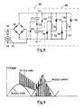
- Figure 8 shows the valley-fill circuit 67 of Figure 6 applied to the converter circuit 69 of a polyphase switched reluctance drive.
- the machine has two phases and the appropriate power switches 71. 72, 76 and 77 are connected to the windings 16 to switch them across the DC link at the appropriate times.
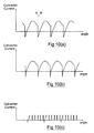
- the circuit of Figure 8 provides two phases, which are switched 180° apart from each other. Each phase, when switched in the normal single-pulse mode, has a current of the general shape of Figure 3(b). When these combine, the current in the DC link has the form shown in Figure 10(a). This would lead to unstable operation of the circuit of Figure 8, for two reasons. Firstly, the abrupt switching of the current from a finite value to zero at point A in the cycle would cause difficulties associated with the supply inductance. The supply current, flowing through the supply inductance, would cause a rise in voltage on the DC link. This is shown by the large voltage spikes in Figure 9 which shows the approximate voltage appearing on the DC link. The voltage would rise until the energy stored in the supply inductor was transferred into the capacitors C1 and C2.
- the phases of the machine are switched so that there is always at least one phase drawing current from the DC link and the current drawn from the DC link is substantially always positive. then the power factor of the drive can be optimised.
- the invention is most beneficial when there are many cycles of operation of the switched reluctance drive occurring within one cycle of the mains supply (eg as shown in Figure 11). This is achieved either by operating a low-pole-number machine at high speed or by operating a high-pole-number machine at lower speeds.
- the single-pulse waveform of Figure 10(b) corresponds to maximum power being drawn by the drive.
- the prior art method of reducing the power output of the drive would be to reduce the conduction angle. As explained above, this would cause an overvoltage of the capacitors C1 and C2 and could not be tolerated.
- the requirement to maintain conduction in at least one phase at all times can be met at lower output powers by using chopping control of the current while still maintaining a fully open conduction angle ie 180° electrical.
- Figure 10(c) shows a typical converter current in a soft chopping mode of control. where five chopping cycles are used in a single conduction cycle. The returned current is very small and is easily handled by the capacitors C1 and C2. While this method of chopping control is detrimental to the overall power factor of the drive (because the supply current is significantly discontinuous), the mode is only used at low powers, where the limit on absolute current level is not generally of concern.
- a control scheme can be implemented for a switched reluctance drive that allows the circuit shown in Figure 8 to be operated such that its power factor is a maximum at maximum power output from the drive.
- a power factor above 0.9 is achievable, allowing a 1650W appliance to be operated from a 120V 15A suppled. Operation at lower power (albeit with reduced power factor) can also be achieved within the supply current limit.
- the illustrative embodiment described above uses a 2-phase switched reluctance drive, but any higher phase number could also be used, since the increased number of phases makes it easier to ensure that there is always a net current drawn from the DC link.
Landscapes
- Engineering & Computer Science (AREA)
- Power Engineering (AREA)
- Rectifiers (AREA)
- Control Of Electric Motors In General (AREA)
- Control Of Electrical Variables (AREA)
Applications Claiming Priority (2)
| Application Number | Priority Date | Filing Date | Title |
|---|---|---|---|
| GBGB9818878.2A GB9818878D0 (en) | 1998-08-28 | 1998-08-28 | Switched reluctance drive with high power factor |
| GB9818878 | 1998-08-28 |
Publications (3)
| Publication Number | Publication Date |
|---|---|
| EP0982845A2 true EP0982845A2 (fr) | 2000-03-01 |
| EP0982845A3 EP0982845A3 (fr) | 2000-05-24 |
| EP0982845B1 EP0982845B1 (fr) | 2011-09-28 |
Family
ID=10838052
Family Applications (1)
| Application Number | Title | Priority Date | Filing Date |
|---|---|---|---|
| EP99306834A Expired - Lifetime EP0982845B1 (fr) | 1998-08-28 | 1999-08-27 | Entraînement à reluctance commandé avec facteur de puissance élevée |
Country Status (8)
| Country | Link |
|---|---|
| US (1) | US6201368B1 (fr) |
| EP (1) | EP0982845B1 (fr) |
| JP (1) | JP2000078884A (fr) |
| KR (1) | KR100671853B1 (fr) |
| CN (1) | CN1093333C (fr) |
| BR (1) | BR9904019A (fr) |
| GB (1) | GB9818878D0 (fr) |
| TW (1) | TW527762B (fr) |
Cited By (2)
| Publication number | Priority date | Publication date | Assignee | Title |
|---|---|---|---|---|
| WO2008113893A3 (fr) * | 2007-03-21 | 2009-02-05 | Kwh Mirka Ab Oy | Machine à poncer électrique compacte |
| KR101879670B1 (ko) * | 2018-02-08 | 2018-07-18 | 스마트론파워(주) | 초기 기동전류를 저감시킨 컨버터 |
Families Citing this family (28)
| Publication number | Priority date | Publication date | Assignee | Title |
|---|---|---|---|---|
| GB0028602D0 (en) * | 2000-11-23 | 2001-01-10 | Switched Reluctance Drives Ltd | Operation of switched reluctance drive systems from dual voltage sources |
| GB0114531D0 (en) * | 2001-06-14 | 2001-08-08 | Switched Reluctance Drives Ltd | A control strategy for switched reluctance drive systems |
| TW200404402A (en) * | 2002-05-24 | 2004-03-16 | Virginia Tech Intell Prop | Apparatus for drive control, power conversion, and start-up control in a PMBDCM or two-phase SRM drive system |
| GB0215849D0 (en) * | 2002-07-09 | 2002-08-14 | Switched Reluctance Drives Ltd | Starting of switched reluctance generators |
| GB2396491B (en) * | 2002-12-21 | 2005-11-30 | Dyson Ltd | Power conversion apparatus |
| GB2410847A (en) * | 2004-02-05 | 2005-08-10 | Dyson Ltd | Control of motor winding energisation according to rotor angle |
| WO2006039626A2 (fr) * | 2004-10-01 | 2006-04-13 | Virginia Tech Intellectual Properties, Inc. | Systeme et procede de commande de fonctionnement a quatre quadrants d'un entrainement par moteur a reluctance commute au moyen d'un commutateur pouvant etre commande, unique |
| FI126995B (sv) * | 2007-03-21 | 2017-09-15 | Mirka Oy | Kompakt elektrisk slipmaskin |
| KR100871391B1 (ko) * | 2007-09-21 | 2008-12-02 | (주)애버드세미컨 | 배압회로를 이용한 고역률 안정기 전원회로 |
| GB2467551B (en) * | 2009-02-05 | 2011-05-18 | Restech Ltd | Electromagnetic field energy recycling |
| US8482214B2 (en) * | 2009-04-24 | 2013-07-09 | City University Of Hong Kong | Apparatus and methods of operation of passive LED lighting equipment |
| US20100321968A1 (en) * | 2009-06-18 | 2010-12-23 | Hamilton Sundstrand Corporation | Load fault handling for switched reluctance or induction type machines |
| TWI396368B (zh) * | 2009-11-19 | 2013-05-11 | Delta Electronics Inc | 整合式多電感磁性組件及多迴路式功率因數校正電路 |
| US9312733B2 (en) * | 2010-11-03 | 2016-04-12 | Regal Beloit America, Inc. | High power density SRM |
| CN102545643B (zh) * | 2012-03-12 | 2014-08-06 | 韩亚兰 | 一种自然续流的交流斩波主电路结构 |
| TWI492502B (zh) | 2012-07-24 | 2015-07-11 | Ind Tech Res Inst | 被動式功因校正電路 |
| TWI469479B (zh) | 2012-08-27 | 2015-01-11 | Ind Tech Res Inst | 被動式功率因數校正電路、應用其之電子裝置與其操作方法 |
| KR101334745B1 (ko) * | 2012-09-03 | 2013-11-29 | 원광대학교산학협력단 | 스위치드 릴럭턴스 모터의 스위칭 각 제어장치 |
| US10348172B2 (en) | 2013-11-13 | 2019-07-09 | Brooks Automation, Inc. | Sealed switched reluctance motor |
| TWI695447B (zh) | 2013-11-13 | 2020-06-01 | 布魯克斯自動機械公司 | 運送設備 |
| KR20230116962A (ko) | 2013-11-13 | 2023-08-04 | 브룩스 오토메이션 인코퍼레이티드 | 브러쉬리스 전기 기계 제어 방법 및 장치 |
| WO2015073647A1 (fr) | 2013-11-13 | 2015-05-21 | Brooks Automation, Inc. | Mécanisme d'entraînement de robot scellé |
| US20150365035A1 (en) * | 2014-06-16 | 2015-12-17 | Samsung Electro-Mechanics Co. Ltd. | Apparatus for driving switched reluctance motor and method of controlling the apparatus |
| CN106114228A (zh) * | 2016-07-21 | 2016-11-16 | 安徽皖南新维电机有限公司 | 一种新能源汽车用高比功率永磁同步磁阻驱动电机系统 |
| BR112022013754A2 (pt) * | 2020-01-14 | 2022-10-11 | Adventech Llc | Métodos para estabelecer uma rede de dispositivos elétricos eficientemente energizados e para fornecer um motor de indução operacionalmente estável, rede de dispositivos elétricos eficientemente energizados, motor de indução, e, sistema de motor de indução de enrolamento reverso de partida progressiva. |
| KR102357021B1 (ko) * | 2021-04-05 | 2022-02-08 | 김주경 | 역률 보상 조명 장치 |
| CN113422551B (zh) * | 2021-05-31 | 2022-06-21 | 江苏大学 | 一种带功率因数校正的开关磁阻电机速度控制系统 |
| CN115940733B (zh) * | 2023-01-18 | 2025-10-24 | 华中科技大学 | 基于带悬浮电容拓扑的同步磁阻电机功率因数改善方法 |
Family Cites Families (9)
| Publication number | Priority date | Publication date | Assignee | Title |
|---|---|---|---|---|
| JPH0365094A (ja) | 1989-08-03 | 1991-03-20 | Secoh Giken Inc | トルクリプルを除去したリラクタンス型電動機 |
| GB9211685D0 (en) * | 1992-06-03 | 1992-07-15 | Switched Reluctance Drives Ltd | Sensorless rotor position measurement |
| CA2103425A1 (fr) | 1992-12-14 | 1994-06-15 | Kurt W. Haas | Circuit a facteur de puissance eleve pour alimenter une charge |
| FR2743955B1 (fr) * | 1996-01-22 | 1998-04-10 | Moulinex Sa | Procede pour alimenter un moteur a reluctance variable a commutation electronique et circuit d'alimentation pour sa mise en oeuvre |
| FR2744577B1 (fr) * | 1996-02-06 | 1998-04-24 | Moulinex Sa | Procede pour alimenter un moteur electrique a reluctance variable a commutation electronique, et circuit d'alimentation pour sa mise en oeuvre |
| GB9608832D0 (en) * | 1996-04-30 | 1996-07-03 | Switched Reluctance Drives Ltd | Power factor correction circuit |
| US5828195A (en) * | 1996-08-29 | 1998-10-27 | Universal Instruments Corporation | Method and apparatus for electronic braking of an electric motor having no permanent magnets |
| GB9713136D0 (en) * | 1997-06-20 | 1997-08-27 | Switched Reluctance Drives Ltd | Switching circuit for a reluctance machine |
| US5994869A (en) * | 1997-12-05 | 1999-11-30 | General Electric Company | Power conversion circuit for a motor |
-
1998
- 1998-08-28 GB GBGB9818878.2A patent/GB9818878D0/en not_active Ceased
- 1998-10-14 TW TW087117019A patent/TW527762B/zh not_active IP Right Cessation
-
1999
- 1999-08-25 CN CN99118081A patent/CN1093333C/zh not_active Expired - Fee Related
- 1999-08-26 KR KR1019990035648A patent/KR100671853B1/ko not_active Expired - Fee Related
- 1999-08-26 JP JP11240505A patent/JP2000078884A/ja active Pending
- 1999-08-27 EP EP99306834A patent/EP0982845B1/fr not_active Expired - Lifetime
- 1999-08-27 BR BR9904019-0A patent/BR9904019A/pt not_active IP Right Cessation
- 1999-08-30 US US09/385,772 patent/US6201368B1/en not_active Expired - Lifetime
Cited By (5)
| Publication number | Priority date | Publication date | Assignee | Title |
|---|---|---|---|---|
| WO2008113893A3 (fr) * | 2007-03-21 | 2009-02-05 | Kwh Mirka Ab Oy | Machine à poncer électrique compacte |
| EP2478998A1 (fr) * | 2007-03-21 | 2012-07-25 | Oy Kwh Mirka Ab | Methode de contrôle pour une machine à poncer électrique |
| RU2484938C2 (ru) * | 2007-03-21 | 2013-06-20 | Ой Квх Мирка Аб | Малогабаритная электрическая шлифовальная машина |
| EP3385031A3 (fr) * | 2007-03-21 | 2018-11-14 | Mirka Oy | Procédé de contrôle d'une machine de meulage électrique |
| KR101879670B1 (ko) * | 2018-02-08 | 2018-07-18 | 스마트론파워(주) | 초기 기동전류를 저감시킨 컨버터 |
Also Published As
| Publication number | Publication date |
|---|---|
| EP0982845A3 (fr) | 2000-05-24 |
| GB9818878D0 (en) | 1998-10-21 |
| EP0982845B1 (fr) | 2011-09-28 |
| TW527762B (en) | 2003-04-11 |
| US6201368B1 (en) | 2001-03-13 |
| CN1246753A (zh) | 2000-03-08 |
| KR100671853B1 (ko) | 2007-01-22 |
| BR9904019A (pt) | 2000-08-01 |
| KR20000017563A (ko) | 2000-03-25 |
| JP2000078884A (ja) | 2000-03-14 |
| CN1093333C (zh) | 2002-10-23 |
Similar Documents
| Publication | Publication Date | Title |
|---|---|---|
| EP0982845B1 (fr) | Entraînement à reluctance commandé avec facteur de puissance élevée | |
| US6646406B1 (en) | Electrical machines | |
| US5994869A (en) | Power conversion circuit for a motor | |
| EP0802623B1 (fr) | Circuit convertisseur pour charge inductive polyphasée commutée | |
| EP1441435B1 (fr) | Générateur de réluctance variable | |
| US6297613B1 (en) | Control of line harmonics | |
| WO2013112981A1 (fr) | Circuit pour transfert de puissance entre une ligne à courant continu et une ligne à courant alternatif | |
| JP2003530810A (ja) | 電気器具用電源 | |
| US5764019A (en) | Control circuit and system for a switched reluctance machine and method of operating | |
| US7372232B2 (en) | Apparatus for drive control, power conversion, and start-up control in a PMBDCM or two-phase SRM drive system | |
| JPH09117183A (ja) | 動力発生装置 | |
| Clothier et al. | Inverter topologies and current sensing methods for short pitched and fully pitched winding SR motors | |
| JPH11206130A (ja) | 電源装置 | |
| Nedic et al. | Experimental verification of induced voltage self-excitation of a switched reluctance generator | |
| US6906490B2 (en) | Starting of switched reluctance generators | |
| MXPA99007807A (en) | Switched reluctance drive with high power factor | |
| Singh et al. | A Bridgeless High Step Down Voltage Gain Based Power Factor Correction Rectifier Fed Low Voltage Low Power Switched Reluctance Motor Drive | |
| Lee et al. | A variable voltage converter topology for permanent-magnet brushless DC motor drives using buck-boost front-end power stage | |
| Srinivas et al. | Evaluation of Power Converter Architectures for Switched Reluctance Motor | |
| Deepika et al. | A PFC BASED BRIDGELESS ZETA CONVERTER FED BLDC MOTOR DRIVE |
Legal Events
| Date | Code | Title | Description |
|---|---|---|---|
| PUAI | Public reference made under article 153(3) epc to a published international application that has entered the european phase |
Free format text: ORIGINAL CODE: 0009012 |
|
| AK | Designated contracting states |
Kind code of ref document: A2 Designated state(s): DE FR GB IT |
|
| AX | Request for extension of the european patent |
Free format text: AL;LT;LV;MK;RO;SI |
|
| PUAL | Search report despatched |
Free format text: ORIGINAL CODE: 0009013 |
|
| AK | Designated contracting states |
Kind code of ref document: A3 Designated state(s): AT BE CH CY DE DK ES FI FR GB GR IE IT LI LU MC NL PT SE |
|
| AX | Request for extension of the european patent |
Free format text: AL;LT;LV;MK;RO;SI |
|
| 17P | Request for examination filed |
Effective date: 20001102 |
|
| AKX | Designation fees paid |
Free format text: DE FR GB IT |
|
| 17Q | First examination report despatched |
Effective date: 20071017 |
|
| GRAP | Despatch of communication of intention to grant a patent |
Free format text: ORIGINAL CODE: EPIDOSNIGR1 |
|
| RIC1 | Information provided on ipc code assigned before grant |
Ipc: H02P 25/08 20060101AFI20110114BHEP |
|
| RAP1 | Party data changed (applicant data changed or rights of an application transferred) |
Owner name: NIDEC SR DRIVES LIMITED |
|
| GRAS | Grant fee paid |
Free format text: ORIGINAL CODE: EPIDOSNIGR3 |
|
| RAP1 | Party data changed (applicant data changed or rights of an application transferred) |
Owner name: NIDEC SR DRIVES LTD. |
|
| RIN1 | Information on inventor provided before grant (corrected) |
Inventor name: WEBSTER, PAUL |
|
| GRAA | (expected) grant |
Free format text: ORIGINAL CODE: 0009210 |
|
| AK | Designated contracting states |
Kind code of ref document: B1 Designated state(s): DE FR GB IT |
|
| REG | Reference to a national code |
Ref country code: GB Ref legal event code: FG4D |
|
| REG | Reference to a national code |
Ref country code: DE Ref legal event code: R096 Ref document number: 69943737 Country of ref document: DE Effective date: 20111117 |
|
| PLBE | No opposition filed within time limit |
Free format text: ORIGINAL CODE: 0009261 |
|
| STAA | Information on the status of an ep patent application or granted ep patent |
Free format text: STATUS: NO OPPOSITION FILED WITHIN TIME LIMIT |
|
| 26N | No opposition filed |
Effective date: 20120629 |
|
| REG | Reference to a national code |
Ref country code: DE Ref legal event code: R097 Ref document number: 69943737 Country of ref document: DE Effective date: 20120629 |
|
| PGFP | Annual fee paid to national office [announced via postgrant information from national office to epo] |
Ref country code: DE Payment date: 20140826 Year of fee payment: 16 |
|
| PGFP | Annual fee paid to national office [announced via postgrant information from national office to epo] |
Ref country code: FR Payment date: 20140820 Year of fee payment: 16 |
|
| PGFP | Annual fee paid to national office [announced via postgrant information from national office to epo] |
Ref country code: IT Payment date: 20140825 Year of fee payment: 16 |
|
| REG | Reference to a national code |
Ref country code: DE Ref legal event code: R119 Ref document number: 69943737 Country of ref document: DE |
|
| PG25 | Lapsed in a contracting state [announced via postgrant information from national office to epo] |
Ref country code: IT Free format text: LAPSE BECAUSE OF NON-PAYMENT OF DUE FEES Effective date: 20150827 |
|
| REG | Reference to a national code |
Ref country code: FR Ref legal event code: ST Effective date: 20160429 |
|
| PG25 | Lapsed in a contracting state [announced via postgrant information from national office to epo] |
Ref country code: DE Free format text: LAPSE BECAUSE OF NON-PAYMENT OF DUE FEES Effective date: 20160301 |
|
| PG25 | Lapsed in a contracting state [announced via postgrant information from national office to epo] |
Ref country code: FR Free format text: LAPSE BECAUSE OF NON-PAYMENT OF DUE FEES Effective date: 20150831 |
|
| PGFP | Annual fee paid to national office [announced via postgrant information from national office to epo] |
Ref country code: GB Payment date: 20170721 Year of fee payment: 19 |
|
| GBPC | Gb: european patent ceased through non-payment of renewal fee |
Effective date: 20180827 |
|
| PG25 | Lapsed in a contracting state [announced via postgrant information from national office to epo] |
Ref country code: GB Free format text: LAPSE BECAUSE OF NON-PAYMENT OF DUE FEES Effective date: 20180827 |