EP0982891A1 - Vorrichtung zum Ein-Ausfügen eines optischen Wellenlängenmultiplexsignales - Google Patents
Vorrichtung zum Ein-Ausfügen eines optischen Wellenlängenmultiplexsignales Download PDFInfo
- Publication number
- EP0982891A1 EP0982891A1 EP99402064A EP99402064A EP0982891A1 EP 0982891 A1 EP0982891 A1 EP 0982891A1 EP 99402064 A EP99402064 A EP 99402064A EP 99402064 A EP99402064 A EP 99402064A EP 0982891 A1 EP0982891 A1 EP 0982891A1
- Authority
- EP
- European Patent Office
- Prior art keywords
- extraction
- filter
- signal
- port
- circuit
- Prior art date
- Legal status (The legal status is an assumption and is not a legal conclusion. Google has not performed a legal analysis and makes no representation as to the accuracy of the status listed.)
- Granted
Links
- 230000003287 optical effect Effects 0.000 title claims abstract description 76
- 238000003780 insertion Methods 0.000 claims abstract description 110
- 230000037431 insertion Effects 0.000 claims abstract description 110
- 238000000605 extraction Methods 0.000 claims abstract description 109
- 230000005540 biological transmission Effects 0.000 claims abstract description 10
- 230000003247 decreasing effect Effects 0.000 claims abstract description 7
- 239000000284 extract Substances 0.000 claims description 4
- 239000000835 fiber Substances 0.000 claims description 4
- 230000008054 signal transmission Effects 0.000 claims description 3
- 238000011144 upstream manufacturing Methods 0.000 claims description 3
- 238000010586 diagram Methods 0.000 description 3
- 230000003321 amplification Effects 0.000 description 1
- 230000000712 assembly Effects 0.000 description 1
- 238000000429 assembly Methods 0.000 description 1
- 239000000470 constituent Substances 0.000 description 1
- 238000001914 filtration Methods 0.000 description 1
- 238000003286 fusion draw glass process Methods 0.000 description 1
- 238000002955 isolation Methods 0.000 description 1
- 238000003199 nucleic acid amplification method Methods 0.000 description 1
- 238000005457 optimization Methods 0.000 description 1
Images

Classifications
-
- H—ELECTRICITY
- H04—ELECTRIC COMMUNICATION TECHNIQUE
- H04Q—SELECTING
- H04Q11/00—Selecting arrangements for multiplex systems
- H04Q11/0001—Selecting arrangements for multiplex systems using optical switching
- H04Q11/0005—Switch and router aspects
-
- H—ELECTRICITY
- H04—ELECTRIC COMMUNICATION TECHNIQUE
- H04J—MULTIPLEX COMMUNICATION
- H04J14/00—Optical multiplex systems
- H04J14/02—Wavelength-division multiplex systems
- H04J14/0201—Add-and-drop multiplexing
- H04J14/0202—Arrangements therefor
- H04J14/0206—Express channels arrangements
-
- H—ELECTRICITY
- H04—ELECTRIC COMMUNICATION TECHNIQUE
- H04J—MULTIPLEX COMMUNICATION
- H04J14/00—Optical multiplex systems
- H04J14/02—Wavelength-division multiplex systems
- H04J14/0201—Add-and-drop multiplexing
- H04J14/0202—Arrangements therefor
- H04J14/021—Reconfigurable arrangements, e.g. reconfigurable optical add/drop multiplexers [ROADM] or tunable optical add/drop multiplexers [TOADM]
- H04J14/0212—Reconfigurable arrangements, e.g. reconfigurable optical add/drop multiplexers [ROADM] or tunable optical add/drop multiplexers [TOADM] using optical switches or wavelength selective switches [WSS]
-
- H—ELECTRICITY
- H04—ELECTRIC COMMUNICATION TECHNIQUE
- H04J—MULTIPLEX COMMUNICATION
- H04J14/00—Optical multiplex systems
- H04J14/02—Wavelength-division multiplex systems
- H04J14/0201—Add-and-drop multiplexing
- H04J14/0215—Architecture aspects
- H04J14/0219—Modular or upgradable architectures
-
- H—ELECTRICITY
- H04—ELECTRIC COMMUNICATION TECHNIQUE
- H04J—MULTIPLEX COMMUNICATION
- H04J14/00—Optical multiplex systems
- H04J14/02—Wavelength-division multiplex systems
- H04J14/0221—Power control, e.g. to keep the total optical power constant
- H04J14/02216—Power control, e.g. to keep the total optical power constant by gain equalization
-
- H—ELECTRICITY
- H04—ELECTRIC COMMUNICATION TECHNIQUE
- H04J—MULTIPLEX COMMUNICATION
- H04J14/00—Optical multiplex systems
- H04J14/02—Wavelength-division multiplex systems
- H04J14/0201—Add-and-drop multiplexing
- H04J14/0202—Arrangements therefor
- H04J14/0213—Groups of channels or wave bands arrangements
-
- H—ELECTRICITY
- H04—ELECTRIC COMMUNICATION TECHNIQUE
- H04Q—SELECTING
- H04Q11/00—Selecting arrangements for multiplex systems
- H04Q11/0001—Selecting arrangements for multiplex systems using optical switching
- H04Q11/0005—Switch and router aspects
- H04Q2011/0007—Construction
- H04Q2011/0009—Construction using wavelength filters
-
- H—ELECTRICITY
- H04—ELECTRIC COMMUNICATION TECHNIQUE
- H04Q—SELECTING
- H04Q11/00—Selecting arrangements for multiplex systems
- H04Q11/0001—Selecting arrangements for multiplex systems using optical switching
- H04Q11/0005—Switch and router aspects
- H04Q2011/0007—Construction
- H04Q2011/0016—Construction using wavelength multiplexing or demultiplexing
-
- H—ELECTRICITY
- H04—ELECTRIC COMMUNICATION TECHNIQUE
- H04Q—SELECTING
- H04Q11/00—Selecting arrangements for multiplex systems
- H04Q11/0001—Selecting arrangements for multiplex systems using optical switching
- H04Q11/0005—Switch and router aspects
- H04Q2011/0007—Construction
- H04Q2011/0022—Construction using fibre gratings
-
- H—ELECTRICITY
- H04—ELECTRIC COMMUNICATION TECHNIQUE
- H04Q—SELECTING
- H04Q11/00—Selecting arrangements for multiplex systems
- H04Q11/0001—Selecting arrangements for multiplex systems using optical switching
- H04Q11/0005—Switch and router aspects
- H04Q2011/0007—Construction
- H04Q2011/0024—Construction using space switching
-
- H—ELECTRICITY
- H04—ELECTRIC COMMUNICATION TECHNIQUE
- H04Q—SELECTING
- H04Q11/00—Selecting arrangements for multiplex systems
- H04Q11/0001—Selecting arrangements for multiplex systems using optical switching
- H04Q11/0005—Switch and router aspects
- H04Q2011/0037—Operation
- H04Q2011/0049—Crosstalk reduction; Noise; Power budget
Definitions
- the invention relates to a device for inserting / extracting optical signals. wavelength multiplexed.
- This device is intended to be associated with a optical link transmitting a multiplex signal to allow it to be extracted some of the multiplexed optical signals and substituting other signals optical by exploiting the wavelengths left available by the signals extracts.
- Insertion and extraction of optical signals of determined wavelengths are essential operations for the communication of information in networks connecting geographically dispersed users.
- he devices for injecting optical signals therefore exist for this purpose in multiplex signal transmission channels which are established at predetermined wavelengths and selectively retrieve information transmitted by the different channels.
- These extraction / insertion devices are in particular intended to equip branching units placed in selected locations of networks to allow selective services of users.
- the signals which pass through a device extraction / insertion by channels of a multiplex signal, without undergoing extraction or insertion, do not follow the same path as those which are locally inserted into channels freed by extracted signals. They are not therefore not affected by the same insertion losses, which results in power level differences for signals transmitted through channels different from a multiplex signal appearing at the output of a device extraction / insertion. It is therefore important to avoid loss of insertion penalizing cannot appear because of a device for some of the multiplexed optical signals which it transmits.
- the invention therefore provides a device for extracting / inserting optical signals wavelength multiplexed with an input and an output for a multiplex signal between which processing circuits are inserted and each allow the extraction of an optical signal contained in one of "N" of "M” channels of incoming optical multiplex signal and insertion of an optical signal in the multiplex signal channel which is left available by the extracted signal.
- each processing circuit comprises a optical extraction filter and an optical signal insertion filter for a channel individual corresponding to a determined wavelength, as well as a individual optical switch to which an extraction port of the extraction filter, an insertion port for the insertion filter, as well as an inlet individual insertion and an individual extraction output from the device, purposes of extraction / insertion into a channel.
- the circuit extraction filters are connected in series, from the input of the device and in decreasing order of lengths waveform in an extraction assembly at the output of which the filters circuits are connected in series and in decreasing order of lengths waveform in an insert set.
- Signal output port multiplex of each filter is connected to the multiplex signal input of the filter following in series, between the input and output of the device to which the input port of the first extraction filter and the last insertion filter are respectively connected.
- IL_drop corresponding to the extraction losses for an extraction filter, IL_sw corresponding to the losses occurring at the level of an optical switch traversed.
- IL_add corresponding to the insertion losses for an insertion filter and IL_thru corresponding to the transit losses occurring between the multiplex signal input port and the multiplex signal output port of an extraction or insertion filter.
- a rejection filter is incorporated in each circuit, downstream of the multiplex signal output port of the extraction filter of the circuit, to increase the level of rejection vis-à-vis the optical signal which is extracted there, this filter being inserted, either directly between this output port and the multiplex signal input port of the extraction or insertion filter, immediately following, for every second extraction filter from the first of serial, either between the input port of the circuit insertion filter and the output port of the immediately preceding insertion or extraction filter to which this filter rejection is then connected by its input port.
- each circuit comprises two rejection filters to increase the rejection level of the circuit vis-à-vis of the optical signal extracted therefrom, these two filters being connected one downstream of the multiplex signal output port of the circuit extraction filter as a whole and the other upstream of the input port of the circuit insertion filter in the insert set.
- a fixed attenuator for adjusting level is inserted between the output of the extraction assembly through which the multiplex signal from the last extraction filter and the input port of the first filter of the insertion set by which this multiplex signal is received.
- a circuit for treatment includes an extraction filter whose extraction port is connected to a first optical divider to allow simultaneous transmission of the optical signal which it extracts, on the one hand, to the circuit insertion filter for reinsertion in the multiplex signal leaving the device and on the other hand, at a individual device extraction output which is assigned to the circuit.
- a processing circuit comprises a second optical splitter which is connected to an individual signal insertion input of the device to allow simultaneous transmission of the signal received from this input, on the one hand, to the circuit insertion filter and, on the other hand, to an output individual extraction of the device which is assigned to the circuit, this transmission being effected via at least one circuit switch.
- the device comprises optical dividers having two asymmetrical outputs.
- the insertion, extraction and rejection filters are of the multilayer interference filter type, of the IFBG type, of the MZ-IFBG type, or of the fiber coupler type obtained by fusion-drawing and comprising a Bragg network in the central region.
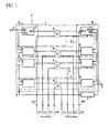
- Figure 1 shows a block diagram of an example device extraction / insertion according to the invention.
- Figure 2 shows a block diagram of a variant device extraction / insertion according to the invention
- FIG. 3 presents a diagram relating to a second variant of the device extraction / insertion according to the invention
- the device 1 for extracting / inserting optical signals multiplexed in length wave which is presented in Figure 1 is designed to receive a multiplex signal optical ⁇ at an input I.
- the multiplex signal ⁇ is composed of a integer "M" of multiplexed optical signals each transmitted by a channel having a determined optical wavelength, different for each channel.
- a number "N" of the "M” multiplexed optical signals of the signal ⁇ , which are transmitted through channels corresponding to wavelengths determined at in advance, are likely to be extracted from this multiplex signal ⁇ by the device extraction / insertion.
- a series of "N" processing circuits 2 is provided in the device extraction / insertion.
- Each of these circuits 2 includes filtering means selective for one of the "N" wavelengths which can be used for extraction / insertion by device 1 and optical switching means to orient the signals likely to be extracted or inserted inside the device.
- each circuit 2 comprises at least one filter extraction module 3, an optical switch 4 and an optical insertion filter 5.
- the extraction filters 3 provided for the different circuits 2 are assumed to identical constitution, they each have a 3E input port for signal multiplex, a 3S1 extraction output port for a signal from a channel determined and a 3S2 transit output port for multiplex signal. They are connected in series between input I of device 1 and output S of a set of extraction 6 which they constitute.
- the first 3E port of entry receives the incoming multiplex signal ⁇ . via entry I.
- the input ports of the other extraction filters 3 are respectively each connected to the transit port 3S2 of the extraction filter which precedes it.
- Each of these other extraction filters receives an optical multiplex signal which corresponds to the multiplex signal ⁇ minus the signal (s) extracted by the filter (s) that precedes it (s) in the extraction assembly 6.
- the insertion filters 5 of the circuits 2 are of identical constitution and they each have a 5E1 insertion port, a 5E2 input port and a 5S output. They are connected in series between an attenuator 7 and the output 0 of the device 1 between which they form an insertion assembly 8.
- the attenuator 7 is connected to the output S of the extraction assembly 6 and the input port 5E2 of the first of the insertion filters 5, in the insertion assembly 8, is connected in downstream of the attenuator 7.
- the port input 5E2 of each of the other insertion filters 5 is connected to the output port 5S of the insertion filter which precedes it in the insertion assembly 8.
- the extraction filters 3 and insertion filters 5 are likely to be filters commonly called IFBG (In Fiber Bragg Grating), comprising networks of Bragg inscribed on fiber. These filters can also be constituted by couplers obtained by melt-drawing and comprising a Bragg grating in their central part, or by Bragg gratings associated with circulators. Of multi-layer interference filters, commonly known as MIFs (Multilayer Interference Filters), can also be provided as envisaged in relation to the variant shown in Figure 2.
- MIFs Multilayer Interference Filters
- the optical switches 4 provided in the processing circuits 2 are by example of switches with two inputs and two outputs.
- a first of inputs of the optical switch 4 of a circuit 2 is connected to the extraction port Circuit filter 3S1 3 to allow signal switching optics extracted by this filter, either to a first of the switch outputs which serves a local extraction port corresponding to 4S1 of device 1, i.e. to a second switch output which is connected to the filter insertion port 5E1 of insertion 5 of the circuit 2 considered.
- the second input of each switch optic 4 is connected to an individual insertion input 4E1 of the device for allow a local optical signal to be substituted for the optical signal which has been extracted by filter 3 from the circuit in the channel previously exploited by this signal extract.
- the signal locally provided by an individual insertion input and transmitted to a 5E1 insertion port can alternatively be switched to the extraction port 4S1 of circuit 2 which includes it, for example for testing purposes, under the control of a control arrangement, not shown, which makes it possible to act on switches 4 of the device.
- processing circuits each allowing local insertion of an optical signal, these signals exploiting wavelengths designated by ⁇ 1 ', ⁇ 2', ⁇ 3 'and ⁇ 4' which are respectively equal to the wavelengths ⁇ 1, ⁇ 2, ⁇ 3, ⁇ 4 used by the signals extracted at device level 1.
- the device 1 according to the invention should preferably be positioned between two amplifiers of the optical multiplex link to which it is associated for extraction / insertion purposes.
- the optical channel wavelength specific to each processing circuit 2 is taken into account when positioning of this circuit in relation to the other circuits 2 in the device 1 who has them.
- This aims to take into account the gain variation depending on the wavelength, commonly referred to by the English expression "gain-tilt", which occurs in an optical amplifier through which transits a multiplex optical signal as envisaged above.
- This gain variation can be considered linear for a power range given in amplifier input and it results in increasing gain in reverse of the wavelength in the considered amplifier.
- Extraction filters 3 from set 6 and insertion filters from set 8 are therefore identically distributed as a function of the wavelength of the channel individual multiplex signal where each of these filters ensures either extraction either an insertion.
- the filter positioned at the head in set 6 or 8 which comprises, is therefore the one which takes into account the individual channel whose length wave is the longest and it is successively followed by the other filters of all distributed by decreasing wavelengths.
- the extraction filter 3 of a processing circuit 2 has the same rank in the extraction assembly 6 of the device which includes it as the insertion filter 5 of the same processing circuit in the insertion assembly 8 of this device.
- the number "N" of processing circuits 2 of a device 1, or of lengths wave that it is likely to exploit, is determined by taking into account the insertion losses affecting the various optical signals when they pass through through filters and switches.
- losses are in particular those which affect the extracted optical signal and the multiplex signal in transit in each extraction filter.
- these losses are those considered to occur between the input port 3E and the extraction port 3S1 for an extracted signal and between this input port 3E and transit port 3S2 for the multiplex signal minus the signal extracted.
- losses are also those which affect on the one hand a signal inserted in a multiplex signal at the level of an insertion filter and on the other hand the multiplex signal which passes through this filter and which undergoes insertion.
- these losses are those considered to occur between the insertion port 5E1 and 5S output port of the filter for the inserted signal and between the input port 5E2 and this same 5S output port in the same filter for the multiplex signal received by this filter.
- IL_agg 2N x IL_thru or IL_thru corresponds to the so-called transit losses occurring between multiplex signal input and multiplex signal output, either between the input port 3E and the transit port 3S2 for an extraction filter 3 or between the input port 5E2 and the 5S output port for an insertion filter 5.
- IL_AD IL_drop + IL_sw + IL_add + (2N - 2 - n) x IL_thru or
- IL_drop corresponds to the so-called extraction losses occurring between the port of entry 3E and the extraction port 3S for an extraction filter 3.
- IL_sw corresponds to the losses occurring at the level of the optical switch 3 crossed.
- IL_add corresponds to the losses occurring between insertion port 5E1 and output port 5S for an insertion filter 5, and or "n" corresponds to the number of filters placed between the transit port 3S2 of an extraction filter and the input port 5E2 of the insertion filter of the same circuit.
- IL_thru 0.7 dB
- IL_sw 1 dB
- the discontinuous nature of this INT (x) function sets the upper limit in the optimization of the uniformization which can be obtained, without imposing excessively rigid constraints as regards the choice of a number N.
- this attenuator acts on the signals multiplexed in length waveform constituting the multiplex signal transmitted from the output S of the assembly extraction 6 to the input port 5E2 of the first insertion filter 5 of the insertion assembly 8, by reducing their level vis-à-vis that of the signals inserted through the different insertion filters 5.
- the first variant presented in FIG. 2 is more particularly planned for the case where the rejection specific to each filter is not sufficient to eliminate any possibility of an optical signal residue being extracted from a channel is added to a signal locally inserted in this channel to be transmitted via the output O of device 1.
- each filter having for example a rejection level of the order of 10 dB.
- rejection filter 9 in each circuit of treatment 2 'so as to raise the overall rejection level of the circuit.
- rejection filters 9 of the multi-layer interference type. This overall rejection level obtained by processing circuit is then of the order 30 dB, which is considered sufficient.
- These filters are either of the type of those previously mentioned above, namely filters called MZ-IFBG (Mach-Zehnder In Fiber Bragg Grating) in which Bragg grids are registered in a fiber Mach-Zehnder structure.
- the rejection filters 9 of a device 1 ' are distributed alternately between the two extraction assemblies 6 'and 8 'of the device, for example one downstream of the extraction filters odd rank and the other upstream of the even rank insertion filters.
- the rejection filter 9 of the first circuit 2 ' is placed in the extraction assembly 6 'between the transit port 3S2 of the extraction filter 3 of this first circuit and the input port 3E of the extraction filter 3 of the circuit 2 'which follows it and therefore corresponds to the wavelength immediately below that of the first circuit.
- the rejection filter 9 of the second circuit is placed in the assembly 8 'between the output port 5S of the extraction filter 3 of the first circuit and the input port 5E2 of the insertion filter 5 of the following circuit 2 'which includes it and so on for the other rejection filters according to the odd or even rank of the circuit which includes them respectively.
- each rejection filter 9 is connected by an input port 9E, through which it receives the multiplex signal transmitted to it by filter 3 or 5 that it follows, and by an output port 9S to the filter 3 or 5 that it precedes.
- the embodiment, shown in Figure 3 corresponds to a variant of the circuit treatment more particularly provided for insertion / extraction devices where an optical signal multiplexed in wavelength is intended to be simultaneously transmitted in two different directions, one of which is that provided for the multiplex signal from which it comes.
- optical divider 10 between the extraction filter 3 of the processing circuit and one of the two inputs of a first 4 'switch which is differs from switch 4 by the fact that it has only one output active.
- the optical divider 10 which is connected to the extraction port 3S1 of the filter extraction 3 is also connected to one of the two inputs of a second switch 4 ' whose single outlet is linked to an individual 4S1 'extraction outlet of the device which is specific to the circuit.
- the signal received by this optical divider 10 is thus transmitted, on the one hand, to the individual extraction output 4S1 'and, on the other hand part, to the insertion port of the insertion filter 5 of the circuit considered to which the first switch 4 'is connected by its single output.
- a second optical divider 10 ' is inserted in the processing circuit considered between an individual 4E1 'insertion input of the device and a second input of each of the two 4 'switches.
- This second divider allows to transmit an optical signal arriving by the individual insertion input 4E1 ', for purposes transmission via the individual extraction output 4S1 'mentioned above and at for insertion into the multiplex signal received by the insertion filter 5, via its 5E2 input port, this insertion taking place in the channel previously occupied by the signal which was extracted by filter 3 of the same circuit.
- the optical dividers 10 have asymmetrical outputs so that the level of the extracted signal which is fed back by a circuit of processing in the multiplex signal leaving the device, is only very slightly reduced, the level of the extracted signal which is transmitted to the output individual extraction 4S1 'being reduced accordingly to a sufficient value to allow it to be taken into account, for example after an amplification carried out in a manner not shown.
Landscapes
- Engineering & Computer Science (AREA)
- Computer Networks & Wireless Communication (AREA)
- Signal Processing (AREA)
- Optical Communication System (AREA)
- Use Of Switch Circuits For Exchanges And Methods Of Control Of Multiplex Exchanges (AREA)
Applications Claiming Priority (2)
| Application Number | Priority Date | Filing Date | Title |
|---|---|---|---|
| FR9810655 | 1998-08-24 | ||
| FR9810655A FR2782588B1 (fr) | 1998-08-24 | 1998-08-24 | Dispositif d'insertion/extraction de signaux optiques multiplexes en longueur d'onde |
Publications (2)
| Publication Number | Publication Date |
|---|---|
| EP0982891A1 true EP0982891A1 (de) | 2000-03-01 |
| EP0982891B1 EP0982891B1 (de) | 2006-11-22 |
Family
ID=9529844
Family Applications (1)
| Application Number | Title | Priority Date | Filing Date |
|---|---|---|---|
| EP99402064A Expired - Lifetime EP0982891B1 (de) | 1998-08-24 | 1999-08-16 | Vorrichtung zum Ein-Ausfügen eines optischen Wellenlängenmultiplexsignales |
Country Status (6)
| Country | Link |
|---|---|
| US (1) | US6498665B1 (de) |
| EP (1) | EP0982891B1 (de) |
| JP (1) | JP4271789B2 (de) |
| AT (1) | ATE346432T1 (de) |
| DE (1) | DE69934058T2 (de) |
| FR (1) | FR2782588B1 (de) |
Cited By (1)
| Publication number | Priority date | Publication date | Assignee | Title |
|---|---|---|---|---|
| EP1191727A3 (de) * | 2000-09-20 | 2006-06-28 | Siemens Aktiengesellschaft | Modular erweiterbares optisches ADD-DROP-modul |
Families Citing this family (2)
| Publication number | Priority date | Publication date | Assignee | Title |
|---|---|---|---|---|
| KR100759167B1 (ko) * | 2001-09-04 | 2007-09-14 | 엘지노텔 주식회사 | 파장분할 다중화 전송장비의 광채널 스위치 및 그 제어방법 |
| US7634196B2 (en) * | 2004-10-06 | 2009-12-15 | Cisco Technology, Inc. | Optical add/drop multiplexer with reconfigurable add wavelength selective switch |
Citations (7)
| Publication number | Priority date | Publication date | Assignee | Title |
|---|---|---|---|---|
| WO1997008574A1 (en) * | 1995-08-29 | 1997-03-06 | Arroyo Optics, Inc. | Wavelength selective grating assisted optical couplers |
| EP0769859A1 (de) * | 1995-10-19 | 1997-04-23 | PIRELLI CAVI S.p.A. | Optisches, transparentes, selbstheilendes Nachrichtenringnetz |
| US5657406A (en) * | 1994-09-23 | 1997-08-12 | United Technologies Corporation | Efficient optical wavelength multiplexer/de-multiplexer |
| US5712717A (en) * | 1995-03-03 | 1998-01-27 | France Telecom | High isolation, optical add-drop multiplexer |
| WO1998005133A1 (en) * | 1996-07-31 | 1998-02-05 | Pirelli Cavi E Sistemi S.P.A. | Device for adding and dropping optical signals |
| EP0838918A1 (de) * | 1996-10-24 | 1998-04-29 | Alcatel | Vorrichtung zum Ein-und Ausfügen von Wellenlängenmultiplexkanälen |
| WO1998052306A2 (en) * | 1997-05-13 | 1998-11-19 | Nokia Telecommunications Oy | Optical add/drop device |
Family Cites Families (2)
| Publication number | Priority date | Publication date | Assignee | Title |
|---|---|---|---|---|
| US6208443B1 (en) * | 1996-10-03 | 2001-03-27 | International Business Machines Corporation | Dynamic optical add-drop multiplexers and wavelength-routing networks with improved survivability and minimized spectral filtering |
| AU1525799A (en) * | 1997-11-18 | 1999-06-07 | California Institute Of Technology | Sampling of electronic signals using optical pulses |
-
1998
- 1998-08-24 FR FR9810655A patent/FR2782588B1/fr not_active Expired - Fee Related
-
1999
- 1999-08-16 DE DE69934058T patent/DE69934058T2/de not_active Expired - Lifetime
- 1999-08-16 AT AT99402064T patent/ATE346432T1/de not_active IP Right Cessation
- 1999-08-16 EP EP99402064A patent/EP0982891B1/de not_active Expired - Lifetime
- 1999-08-20 US US09/377,747 patent/US6498665B1/en not_active Expired - Lifetime
- 1999-08-23 JP JP23535599A patent/JP4271789B2/ja not_active Expired - Fee Related
Patent Citations (7)
| Publication number | Priority date | Publication date | Assignee | Title |
|---|---|---|---|---|
| US5657406A (en) * | 1994-09-23 | 1997-08-12 | United Technologies Corporation | Efficient optical wavelength multiplexer/de-multiplexer |
| US5712717A (en) * | 1995-03-03 | 1998-01-27 | France Telecom | High isolation, optical add-drop multiplexer |
| WO1997008574A1 (en) * | 1995-08-29 | 1997-03-06 | Arroyo Optics, Inc. | Wavelength selective grating assisted optical couplers |
| EP0769859A1 (de) * | 1995-10-19 | 1997-04-23 | PIRELLI CAVI S.p.A. | Optisches, transparentes, selbstheilendes Nachrichtenringnetz |
| WO1998005133A1 (en) * | 1996-07-31 | 1998-02-05 | Pirelli Cavi E Sistemi S.P.A. | Device for adding and dropping optical signals |
| EP0838918A1 (de) * | 1996-10-24 | 1998-04-29 | Alcatel | Vorrichtung zum Ein-und Ausfügen von Wellenlängenmultiplexkanälen |
| WO1998052306A2 (en) * | 1997-05-13 | 1998-11-19 | Nokia Telecommunications Oy | Optical add/drop device |
Non-Patent Citations (1)
| Title |
|---|
| ANTONIADES N ET AL: "Simulation of ASE noise accumulation in a wavelength add-drop multiplexer cascade", IEEE PHOTONICS TECHNOLOGY LETTERS, SEPT. 1997, IEEE, USA, vol. 9, no. 9, ISSN 1041-1135, pages 1274 - 1276, XP002101306 * |
Cited By (2)
| Publication number | Priority date | Publication date | Assignee | Title |
|---|---|---|---|---|
| EP1191727A3 (de) * | 2000-09-20 | 2006-06-28 | Siemens Aktiengesellschaft | Modular erweiterbares optisches ADD-DROP-modul |
| DE10046585B4 (de) * | 2000-09-20 | 2007-10-25 | Siemens Ag | Modular erweiterbares optisches ADD-DROP-Modul |
Also Published As
| Publication number | Publication date |
|---|---|
| US6498665B1 (en) | 2002-12-24 |
| JP4271789B2 (ja) | 2009-06-03 |
| DE69934058T2 (de) | 2007-08-16 |
| FR2782588B1 (fr) | 2002-12-20 |
| FR2782588A1 (fr) | 2000-02-25 |
| EP0982891B1 (de) | 2006-11-22 |
| ATE346432T1 (de) | 2006-12-15 |
| JP2000078083A (ja) | 2000-03-14 |
| DE69934058D1 (de) | 2007-01-04 |
Similar Documents
| Publication | Publication Date | Title |
|---|---|---|
| EP0730172B1 (de) | Ein optische Zirkulatoren und durch Lichteinstrahlung eingeschriebene Bragg-Gitter verwendender optischer Multiplexer zur Einfügung und Ausblendung von Wellenlängen | |
| US6466341B1 (en) | Add/drop filter for a multi-wavelength lightwave system | |
| EP1879308B1 (de) | Verfahren und Vorrichtung zur Überwachung von optischen Verbindungen in einem transparenten optischen Netzwerk | |
| CA2026658C (fr) | Systeme de communication optique temporel asynchrone | |
| US7151875B2 (en) | Method and apparatus for balancing the power of optical channels traversing an optical add drop multiplexer | |
| EP0838918B1 (de) | Vorrichtung zum Ein-und Ausfügen von Wellenlängenmultiplexkanälen | |
| FR2755807A1 (fr) | Dispositif demultiplexeur pour des communications par fibres optiques, multiplexees par repartition en longueur d'onde | |
| FR2893718A1 (fr) | Dispositif de commutation optique entre des lignes optiques amont et aval, a adjonction de signature de noeud pour le suivi des chemins optiques de connexion | |
| EP1179964A2 (de) | Schalter für optische Signale | |
| EP0982891B1 (de) | Vorrichtung zum Ein-Ausfügen eines optischen Wellenlängenmultiplexsignales | |
| JPH0936834A (ja) | 光分岐挿入回路 | |
| FR2736480A1 (fr) | Disposif de coloration de signaux optiques | |
| EP0802640A1 (de) | Verfahren und Vorrichtung zur Verstärkung von Kanälen aus Wellenlängenmultiplex aufbereitet | |
| EP1355441A1 (de) | Verfahren unf Vorrichtung zum steuern der Übertragung optischer Signale | |
| FR2830709A1 (fr) | Dispositif de commutation selective de frequences et circuit a retard optique reconfigurable l'incorporant | |
| FR2821504A1 (fr) | Dispositif d'extraction de frequence | |
| FR2838568A1 (fr) | Generateur de signaux optiques porteurs de donnees et de longueurs d'onde porteuses selectionnables | |
| EP1326473B1 (de) | Optische Schaltvorrichtung und Kontrolleverfahren dafür | |
| FR2844654A1 (fr) | Peigne de frequences pour reseau a multiplexage par repartition de frequences optiques | |
| EP1193996B1 (de) | Verfahren zum Detektieren von Unterteilungen in WDM Koppelfeld-Knoten | |
| EP1098465A1 (de) | Verfahren zum Abführen von einem Kanal für ein optisches Wellenlängemultiplex-Übertragungsystem und Vorrichtung zur Anwendung dieses Verfahrens | |
| EP1455551A2 (de) | Selektionsmodul für optische Schalter und optischer Schalter | |
| EP2282430B1 (de) | Vorrichtung zum Mehrwege-Abzweigen von WDM-Kanälen | |
| CN1217505C (zh) | 一种光通信网络 | |
| FR2828603A1 (fr) | Systeme de commutation optique tel que brasseur ou routeur pour reseau de transmission |
Legal Events
| Date | Code | Title | Description |
|---|---|---|---|
| PUAI | Public reference made under article 153(3) epc to a published international application that has entered the european phase |
Free format text: ORIGINAL CODE: 0009012 |
|
| AK | Designated contracting states |
Kind code of ref document: A1 Designated state(s): AT BE CH CY DE DK ES FI FR GB GR IE IT LI LU MC NL PT SE |
|
| AX | Request for extension of the european patent |
Free format text: AL;LT;LV;MK;RO;SI |
|
| 17P | Request for examination filed |
Effective date: 20000901 |
|
| AKX | Designation fees paid |
Free format text: AT BE CH CY DE DK ES FI FR GB GR IE IT LI LU MC NL PT SE |
|
| 17Q | First examination report despatched |
Effective date: 20020220 |
|
| GRAP | Despatch of communication of intention to grant a patent |
Free format text: ORIGINAL CODE: EPIDOSNIGR1 |
|
| GRAS | Grant fee paid |
Free format text: ORIGINAL CODE: EPIDOSNIGR3 |
|
| GRAA | (expected) grant |
Free format text: ORIGINAL CODE: 0009210 |
|
| AK | Designated contracting states |
Kind code of ref document: B1 Designated state(s): AT BE CH CY DE DK ES FI FR GB GR IE IT LI LU MC NL PT SE |
|
| PG25 | Lapsed in a contracting state [announced via postgrant information from national office to epo] |
Ref country code: NL Free format text: LAPSE BECAUSE OF FAILURE TO SUBMIT A TRANSLATION OF THE DESCRIPTION OR TO PAY THE FEE WITHIN THE PRESCRIBED TIME-LIMIT Effective date: 20061122 Ref country code: IE Free format text: LAPSE BECAUSE OF FAILURE TO SUBMIT A TRANSLATION OF THE DESCRIPTION OR TO PAY THE FEE WITHIN THE PRESCRIBED TIME-LIMIT Effective date: 20061122 Ref country code: FI Free format text: LAPSE BECAUSE OF FAILURE TO SUBMIT A TRANSLATION OF THE DESCRIPTION OR TO PAY THE FEE WITHIN THE PRESCRIBED TIME-LIMIT Effective date: 20061122 Ref country code: AT Free format text: LAPSE BECAUSE OF FAILURE TO SUBMIT A TRANSLATION OF THE DESCRIPTION OR TO PAY THE FEE WITHIN THE PRESCRIBED TIME-LIMIT Effective date: 20061122 |
|
| REG | Reference to a national code |
Ref country code: GB Ref legal event code: FG4D Free format text: NOT ENGLISH |
|
| REG | Reference to a national code |
Ref country code: CH Ref legal event code: EP |
|
| REG | Reference to a national code |
Ref country code: IE Ref legal event code: FG4D Free format text: LANGUAGE OF EP DOCUMENT: FRENCH |
|
| REF | Corresponds to: |
Ref document number: 69934058 Country of ref document: DE Date of ref document: 20070104 Kind code of ref document: P |
|
| GBT | Gb: translation of ep patent filed (gb section 77(6)(a)/1977) |
Effective date: 20070129 |
|
| PG25 | Lapsed in a contracting state [announced via postgrant information from national office to epo] |
Ref country code: SE Free format text: LAPSE BECAUSE OF FAILURE TO SUBMIT A TRANSLATION OF THE DESCRIPTION OR TO PAY THE FEE WITHIN THE PRESCRIBED TIME-LIMIT Effective date: 20070222 Ref country code: DK Free format text: LAPSE BECAUSE OF FAILURE TO SUBMIT A TRANSLATION OF THE DESCRIPTION OR TO PAY THE FEE WITHIN THE PRESCRIBED TIME-LIMIT Effective date: 20070222 |
|
| PG25 | Lapsed in a contracting state [announced via postgrant information from national office to epo] |
Ref country code: ES Free format text: LAPSE BECAUSE OF FAILURE TO SUBMIT A TRANSLATION OF THE DESCRIPTION OR TO PAY THE FEE WITHIN THE PRESCRIBED TIME-LIMIT Effective date: 20070305 |
|
| PG25 | Lapsed in a contracting state [announced via postgrant information from national office to epo] |
Ref country code: PT Free format text: LAPSE BECAUSE OF FAILURE TO SUBMIT A TRANSLATION OF THE DESCRIPTION OR TO PAY THE FEE WITHIN THE PRESCRIBED TIME-LIMIT Effective date: 20070423 |
|
| NLV1 | Nl: lapsed or annulled due to failure to fulfill the requirements of art. 29p and 29m of the patents act | ||
| RAP2 | Party data changed (patent owner data changed or rights of a patent transferred) |
Owner name: ALCATEL LUCENT |
|
| REG | Reference to a national code |
Ref country code: IE Ref legal event code: FD4D |
|
| REG | Reference to a national code |
Ref country code: FR Ref legal event code: CD |
|
| PLBE | No opposition filed within time limit |
Free format text: ORIGINAL CODE: 0009261 |
|
| STAA | Information on the status of an ep patent application or granted ep patent |
Free format text: STATUS: NO OPPOSITION FILED WITHIN TIME LIMIT |
|
| 26N | No opposition filed |
Effective date: 20070823 |
|
| BERE | Be: lapsed |
Owner name: ALCATEL Effective date: 20070831 |
|
| REG | Reference to a national code |
Ref country code: CH Ref legal event code: PL |
|
| PG25 | Lapsed in a contracting state [announced via postgrant information from national office to epo] |
Ref country code: MC Free format text: LAPSE BECAUSE OF NON-PAYMENT OF DUE FEES Effective date: 20070831 Ref country code: LI Free format text: LAPSE BECAUSE OF NON-PAYMENT OF DUE FEES Effective date: 20070831 Ref country code: GR Free format text: LAPSE BECAUSE OF FAILURE TO SUBMIT A TRANSLATION OF THE DESCRIPTION OR TO PAY THE FEE WITHIN THE PRESCRIBED TIME-LIMIT Effective date: 20070223 Ref country code: CH Free format text: LAPSE BECAUSE OF NON-PAYMENT OF DUE FEES Effective date: 20070831 |
|
| PG25 | Lapsed in a contracting state [announced via postgrant information from national office to epo] |
Ref country code: BE Free format text: LAPSE BECAUSE OF NON-PAYMENT OF DUE FEES Effective date: 20070831 |
|
| PG25 | Lapsed in a contracting state [announced via postgrant information from national office to epo] |
Ref country code: LU Free format text: LAPSE BECAUSE OF NON-PAYMENT OF DUE FEES Effective date: 20070816 Ref country code: CY Free format text: LAPSE BECAUSE OF FAILURE TO SUBMIT A TRANSLATION OF THE DESCRIPTION OR TO PAY THE FEE WITHIN THE PRESCRIBED TIME-LIMIT Effective date: 20061122 |
|
| PGFP | Annual fee paid to national office [announced via postgrant information from national office to epo] |
Ref country code: IT Payment date: 20100823 Year of fee payment: 12 |
|
| PG25 | Lapsed in a contracting state [announced via postgrant information from national office to epo] |
Ref country code: IT Free format text: LAPSE BECAUSE OF NON-PAYMENT OF DUE FEES Effective date: 20110816 |
|
| REG | Reference to a national code |
Ref country code: FR Ref legal event code: GC Effective date: 20140717 |
|
| REG | Reference to a national code |
Ref country code: FR Ref legal event code: CA Effective date: 20150521 |
|
| REG | Reference to a national code |
Ref country code: FR Ref legal event code: CA Effective date: 20150521 |
|
| REG | Reference to a national code |
Ref country code: FR Ref legal event code: PLFP Year of fee payment: 17 |
|
| REG | Reference to a national code |
Ref country code: FR Ref legal event code: PLFP Year of fee payment: 18 |
|
| REG | Reference to a national code |
Ref country code: FR Ref legal event code: PLFP Year of fee payment: 19 |
|
| PGFP | Annual fee paid to national office [announced via postgrant information from national office to epo] |
Ref country code: DE Payment date: 20170822 Year of fee payment: 19 Ref country code: GB Payment date: 20170822 Year of fee payment: 19 Ref country code: FR Payment date: 20170822 Year of fee payment: 19 |
|
| REG | Reference to a national code |
Ref country code: DE Ref legal event code: R119 Ref document number: 69934058 Country of ref document: DE |
|
| GBPC | Gb: european patent ceased through non-payment of renewal fee |
Effective date: 20180816 |
|
| REG | Reference to a national code |
Ref country code: DE Ref legal event code: R082 Ref document number: 69934058 Country of ref document: DE Representative=s name: MENZIETTI WETZEL, DE Ref country code: DE Ref legal event code: R081 Ref document number: 69934058 Country of ref document: DE Owner name: PROVENANCE ASSET GROUP LLC, PITTSFORD, US Free format text: FORMER OWNER: ALCATEL LUCENT, PARIS, FR |
|
| PG25 | Lapsed in a contracting state [announced via postgrant information from national office to epo] |
Ref country code: DE Free format text: LAPSE BECAUSE OF NON-PAYMENT OF DUE FEES Effective date: 20190301 |
|
| PG25 | Lapsed in a contracting state [announced via postgrant information from national office to epo] |
Ref country code: FR Free format text: LAPSE BECAUSE OF NON-PAYMENT OF DUE FEES Effective date: 20180831 |
|
| REG | Reference to a national code |
Ref country code: GB Ref legal event code: 732E Free format text: REGISTERED BETWEEN 20190829 AND 20190904 |
|
| PG25 | Lapsed in a contracting state [announced via postgrant information from national office to epo] |
Ref country code: GB Free format text: LAPSE BECAUSE OF NON-PAYMENT OF DUE FEES Effective date: 20180816 |