EP0983545B1 - Risc-prozessor - Google Patents
Risc-prozessor Download PDFInfo
- Publication number
- EP0983545B1 EP0983545B1 EP98933475A EP98933475A EP0983545B1 EP 0983545 B1 EP0983545 B1 EP 0983545B1 EP 98933475 A EP98933475 A EP 98933475A EP 98933475 A EP98933475 A EP 98933475A EP 0983545 B1 EP0983545 B1 EP 0983545B1
- Authority
- EP
- European Patent Office
- Prior art keywords
- task
- address
- selector switch
- input
- call
- Prior art date
- Legal status (The legal status is an assumption and is not a legal conclusion. Google has not performed a legal analysis and makes no representation as to the accuracy of the status listed.)
- Expired - Lifetime
Links
Images


Classifications
-
- G—PHYSICS
- G06—COMPUTING OR CALCULATING; COUNTING
- G06F—ELECTRIC DIGITAL DATA PROCESSING
- G06F9/00—Arrangements for program control, e.g. control units
- G06F9/06—Arrangements for program control, e.g. control units using stored programs, i.e. using an internal store of processing equipment to receive or retain programs
- G06F9/46—Multiprogramming arrangements
- G06F9/48—Program initiating; Program switching, e.g. by interrupt
- G06F9/4806—Task transfer initiation or dispatching
- G06F9/4843—Task transfer initiation or dispatching by program, e.g. task dispatcher, supervisor, operating system
-
- G—PHYSICS
- G06—COMPUTING OR CALCULATING; COUNTING
- G06F—ELECTRIC DIGITAL DATA PROCESSING
- G06F9/00—Arrangements for program control, e.g. control units
- G06F9/06—Arrangements for program control, e.g. control units using stored programs, i.e. using an internal store of processing equipment to receive or retain programs
- G06F9/46—Multiprogramming arrangements
- G06F9/48—Program initiating; Program switching, e.g. by interrupt
- G06F9/4806—Task transfer initiation or dispatching
- G06F9/4843—Task transfer initiation or dispatching by program, e.g. task dispatcher, supervisor, operating system
- G06F9/485—Task life-cycle, e.g. stopping, restarting, resuming execution
-
- G—PHYSICS
- G06—COMPUTING OR CALCULATING; COUNTING
- G06F—ELECTRIC DIGITAL DATA PROCESSING
- G06F9/00—Arrangements for program control, e.g. control units
- G06F9/06—Arrangements for program control, e.g. control units using stored programs, i.e. using an internal store of processing equipment to receive or retain programs
- G06F9/44—Arrangements for executing specific programs
- G06F9/448—Execution paradigms, e.g. implementations of programming paradigms
- G06F9/4482—Procedural
- G06F9/4484—Executing subprograms
- G06F9/4486—Formation of subprogram jump address
Definitions
- Multi-layered and complex switching procedures or data protocols in switching systems each require modules tailored to their intended use. Pure logic circuits or integrated circuits or reduced instruction set computer (RISC) processors, for example, are then arranged on these modules.
- the switching procedures and data protocols to be processed in the switching systems and in particular in the interface modules are subject to increased requirements with regard to reliability.
- the known RISC processors have the disadvantage that there are errors in the program sequence due to an external influence or program errors, in which the processor is blocked by program loops.
- the usual interrupt controls of the conventional RISC processors restrict the use of these at high processing speeds.
- the invention has for its object a RISC processor Specify architecture and a process in which a Blocking the processor is avoided.
- the invention has the advantage that no persistent Blocking of RISC processor operation by program sequences is possible because after a disturbance by everyone any program address jumped back to the initial state becomes.
- the invention has the advantage that with an implementation of task and function stack's command sequences can be processed safely and quickly.
- FIG. A structure of a RISC processor is shown schematically in FIG. This illustration shows the essential components of a RISC processor arranged in a pipeline. These components are, for example, a sequence controller SC, a function stack FS and a task stack TS, an instruction decoder ID, a register read unit RR, an execute unit E, a data transfer unit DT, a register write unit RW, an input and output unit I / O and a register file RF.
- the sequence controller SC essentially supplies an address for the instruction decoder ID in order to read out an instruction code from an opcode memory.
- the opcode memory is arranged, for example, in an area of a memory chip ROM. From the command code, ID commands CMD1, CMD2,...
- CMDn are formed in the instruction decoder for the individual units of the RISC processor shown in FIG. 1 arranged in the pipeline.
- the commands CMDn are then forwarded from the instruction decoder ID to the left and right to the processing units arranged in the pipeline.
- a command field is created for each of these processing units RR, E, DT, RW or SC.
- command fields for the register read unit RR, for the execute unit E, for the data transfer unit DT and for the register write unit RW go, while to the left the command field is passed on for direct jump commands.
- Direct jump commands are executed by the instruction decoder ID and the sequence controller SC within one cycle.
- a direct (absolute) jump command is issued without delay.
- the commands are read from the register file RF by the register read unit RR and forwarded to the execute unit E.
- the data read from the register file RF are the data that are stored in the register SRC and in the register AluSrc1, AluSrc2 (two operands). All arithmetic and logical instructions are executed in the execute unit E, ie all addition and subtraction instructions as well as all logic operations. Jumps are displayed in the command CMD of the instruction decoder ID. A distinction is made between the commands CMD0, CMD1, CMD2 etc. In addition, there is another variant (indirect jumps) for address determination for branching within a program.
- branching in the processor program is effected via relative jump addresses (rel. Jump).
- the new address is formed via the execute unit E and transferred to the sequence controller SC via a current signal.
- This jump (relative address) is not coded in the instruction decoder ID but is only determined in the execution unit E.
- This command executes a jump command to an absolute address during one clock period and the subsequent processing address is stored in the task stack TS.
- An equivalent removal command for this is the Next command.
- the next command gives a command to the sequence controller SC via the instruction decoder ID, which ensures that a new program address is formed from the address stored in the task stack TS.
- the return command sends a command to the sequence controller SC via the instruction decoder ID, which ensures that a new program address is formed from the address stored in the function stack FS.
- the nesting of the subroutines is limited to two (task, call) (see FIG. 2).
- a further nesting depth can be realized using additional stacks, call commands and return commands.
- the program of the RISC processor is stored in a ROM, for example.
- the program of the processor is constructed in such a way that a task call Tnx is made only via a task table TT and a further function call Funcx is made only from a task Tnx.
- a first return address for the NEXT command is temporarily stored in a task stack TS and a second return address for the RET command is temporarily stored in a function stack FS.
- the first and second return address NEXT, RET are each formed from a subsequent address of a current address when the subroutine is called (see FIG. 3).
- each function Funcx ends with a function return RET and every task Tnx ends with a task return NEXT, it is ensured that there is always a return to the task table TT.
- a nesting depth of 1 for a task and a function means that you can only call one task. No further function or task can be called from the Funcx function. However, additional functions can be called from the task.
- the tasks are processed from a task table TT.
- a task table TT contains additional SYNC commands. When executing a SYNC instruction, the processor is stopped until a SYNC pulse is generated by the hardware.
- a jump address is generated from a timeslot number created by the hardware and points to a new address within the task table TT.
- the first address corresponds to a time slot number TSN.
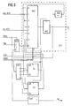
- Fig. 3 shows a program counter PCT.
- This program counter PCT is part of the sequence controller SC.
- the program counter PCT consists of a register RPC, an adder ADD and a first switch, for example a multiplexer MU1.
- the first multiplexer MU1 is controlled with a command CMDn. With a command CMD0 a simple command like Continue, Execute or local Store etc. is executed.
- CMD1 there is an absolute jump
- CMD2 there is a CALL to an absolute address
- CMD3 there is a call for a task with an absolute address
- CMD4 there is a return RET from the function stack FS
- CMD5 a next command from the task stack TS
- CMD6 there is a SYNC command and with CMD 7 a relative jump.
- the command CMDn is first fed to a decoder DEC.
- the read / write control signals are decoded from the commands CMDn in a de-coding unit DEC.
- first and second return addresses are stored in the task stack TS and function stack FS.
- CMD SYNC command
- SYNC current program address
- TSN time slot number
- a sequence controller SC primarily has the task of calculating and providing the next program address PC.
- the sequence controller SC is prepared by the multiplexers MU1 / MU2 for the next SYNC command CMD6 in the task table (task table) to branch into a task TS1, TS2 ...
- the address within the task table TT is determined by the time slot number TSN created from the outside.
- a timer T is additionally started by the sync pulse SYNC, whereby each task TnA, ..., Tnx can decide by its counter reading whether it is still executable before the end of the time slot.
- SYNC command CMD6 the sequence controller SC remains at the current address and waits for a SYNC pulse, after which the sequence controller SC issues a new program address depending on the time slot number TSN.
- the RISC processor receives various commands for the task or function call (CMD2 (TASK) / CMD3 (CALL)) and a corresponding return (CMD4 (NEXT) / CMD5 (RET)) and a SYNC command CMD6 for synchronization with the SYNC pulse with the associated time slot number TSN.
- CMD2 TASK
- CMD3 CMD3
- RET CMD5
- SYNC command CMD6 for synchronization with the SYNC pulse with the associated time slot number TSN.
- the sequence controller SC is provided with two stack registers (function and task stack) FS, TS for storing the return addresses.
Landscapes
- Engineering & Computer Science (AREA)
- Software Systems (AREA)
- Theoretical Computer Science (AREA)
- Physics & Mathematics (AREA)
- General Engineering & Computer Science (AREA)
- General Physics & Mathematics (AREA)
- Executing Machine-Instructions (AREA)
Description
Die bekannten RISC-Prozessoren weisen den Nachteil auf, daß sich durch eine externe Beeinflußung oder Programmfehler im Programmablauf Fehler ergeben, bei denen der Prozessor durch Programmschleifen blockiert wird.
Neben dem genannten Nachteil schränken die üblichen Interruptsteuerungen der herkömmlichen RISC-Prozessoren die Verwendung dieser bei hohen Verarbeitungsgeschwindigkeiten ein.
Sprünge werden im Kommando CMD des Instruction-Decoders ID angezeigt. Dabei wird unterschieden zwischen den Kommandos CMD0, CMD1, CMD2 usw.. Zusätzlich gibt es noch eine weitere Variante (indirekte Sprünge) zur Adressenermittlung für das Verzweigen innerhalb eines Programms. In dieser Variante wird das Verzweigen im Prozessorprogramm über relative Sprungadressen (rel. Jump) bewirkt. Dabei wird die neue Adresse über die Execute-Einheit E gebildet und über ein Strom-Signal dem Sequenz-Controller SC übergegeben. Dieser Sprung (relative Adresse) wird nicht im Instruction-Decoder ID codiert sondern erst in der Execute-Einheit E ermittelt.
Für die Belegung des Function-Stacks FS gibt es ein Kommando. Mit diesem Kommando wird ein Sprungbefehl NEXT während einer Taktperiode auf eine absolute Adresse ausgeführt und die nachfolgende Abarbeitungsadresse im Function-Stack FS abgelegt.
Ein äquivalentes Entfernkommando hierfür ist der Return-Befehl. Durch den Return-Befehl wird über den Instruction-Decoder ID ein Kommando an den Sequence-Controller SC gegeben, das dafür sorgt, daß aus der Adresse die im Function-Stack FS abgelegt ist eine neue Programmadresse gebildet wird.
In diesem Ausführungsbeispiel ist die Verschachtelung der Unterprogramme auf zwei begrenzt (Task, Call) (siehe Fig. 2). Eine weitere Verschachtelungstiefe kann über zusätzliche Stack's, Aufrufbefehle und Returnbefehle realisiert werden.
Die erste Adresse entspricht einer Zeitschlitznummer TSN.
Mit dem oben beschriebenen Programmaufbau wird eine anhaltende Blockierungen bei Programmabläufen wirksam verhindert.
Ein Sequence-Controller SC hat wie bereits beschrieben in erster Linie die Aufgabe die nächste Programmadresse PC zu berechnen und bereitzustellen. Zur Steuerung des Sequence-Controllers SC gibt es mehrere Möglichkeiten:
Durch einen Synchronisierimpuls SYNC zu Beginn eines jeden Zeitschlitzes TSN wird der Sequence-Controller SC durch die Multiplexer MU1/MU2 darauf vorbereitet beim nächsten SYNC-Befehl CMD6 in der Task-Tabelle (Aufgabentabelle) in eine Task TS1, TS2... zu verzweigen. Die Adresse innerhalb der Task-Tabelle TT wird durch die von außen angelegte Zeitschlitznummer TSN bestimmt.
Durch den Synchronimpuls SYNC wird zusätzlich ein Timer T gestartet, wobei durch dessen Zählerstand jede Task TnA,..., Tnx entscheiden kann, ob sie noch vor Ende des Zeitschlitzes ablauffähig ist. Bei einem SYNC-Befehl CMD6 bleibt der Sequence-Controller SC auf der aktuellen Adresse stehen und wartet auf einen SYNC-Impuls danach gibt der Sequence-Controller SC in Abhängigkeit der Zeitschlitznummer TSN auf eine neue Programmadresse. Zur Ausführung der Befehle CMD erhält der RISC-Prozessor unterschiedliche Befehle für den Task- oder Functionsaufruf (CMD2(TASK)/CMD3(CALL)) und einen entsprechenden Rücksprung (CMD4(NEXT)/CMD5 (RET)) sowie ein SYNC-Befehl CMD6 zum Synchronisieren mit dem SYNC-Impuls mit der zugehörigen Zeitschlitznummer TSN. Dem Sequence-Controller SC werden dazu zwei Stack-Register(Function- und Task-Stack) FS, TS für die Speicherung der Rücksprungadressen zur Verfügung gestellt.
Claims (8)
- Verfahren zum Aufrufen von Unterprogrammen bei einem Reduced Instruction Set Computer (RISC)- Prozessor, mit folgenden Verfahrensschritten,
in einem ersten Programmschritt wird mit einer ersten Adresse (TSN) ein von mehreren in einer Task-Tabelle (TT) gespeichertes Programmteil (TSn) aufgerufen,
in einen zweiten Programmschritt wird von der Task-Tabelle (TT) in eine Task (Tna,...Tnx) gesprungen und eine erste Rücksprungadresse (NEXT) ermittelt und in einem separaten Speicher (TS) gespeichert,
nach Abarbeitung der Task (Tna, ... ,Tnx) wird mit Hilfe der gespeicherten ersten Rücksprungadresse (NEXT) zur Task-Tabelle (TT) zurückgesprungen und
daß bei einer weiteren Verzweigung aus der Task (Tna,...,Tnx) in Unterprogramme (Funca,...,Funcx) eine zweite Rücksprungadresse (RET) ermittelt und diese in einem weiteren separaten Speicher (FS) gespeichert wird. - Verfahren nach Anspruch 1,
dadurch gekennzeichnet
daß nach Abarbeitung des Unterprogramms (Funca,..., Funcx) mit Hilfe der gespeicherten zweiten Rücksprungadresse (RET) in die Task (Tnx) zurückgesprungen wird. - Verfahren nach Anspruch 1,
dadurch gekennzeichnet
daß die erste und zweite Rücksprungadresse (NEXT, RET) jeweils die Folgeadresse einer aktuellen Sprungadresse (TaskTnx, Call Funcx) ist. - Verfahren nach Anspruch 1,
dadurch gekennzeichnet,
daß ein Task-Aufruf (TaskTnx) aus der Task-Tabelle TT erfolgt,
daß aus einer Task (T1 A) ein Unterprogramm-Aufruf (Call FUNCX) erfolgt. - Verfahren nach einem der vorhergehenden Ansprüche,
dadurch gekennzeichnet,
daß der erste Programmschritt mit einer ersten Adresse (TSN) ausgeführt wird nachdem ein Sychronimpuls (SYNC) diese freigegeben hat. - Verfahren nach Anspruch 5,
dadurch gekennzeichnet,
daß vor einer Freigabe der ersten Adresse (TSN) ein Timer (T) gestartet wird und je nach Zählerstand des Timers (T) entschieden wird ob eine aufgerufene Task (Tnx) noch vor Ende einer aktuellen Taktperiode abgearbeitet werden kann, oder ob die aufgerufene Task beendet wird. - Anordnung eines Reduced Instruction Set Computer (RISC)-Prozessors mit einem Sequenz-Controller (SC) zur Bereitstellung von Programmadressen, der einen ersten Umschalter (MU1) aufweist, der nach Maßgabe von Kommandos (CMDn) die am Steuereingang des ersten Umschalters anliegen jeweils eine Adresse von den an den Eingängen des ersten Umschalters (MU1) anliegenden Adressen (abs.ADR, rel.ADR,....) an eine nachgeordnete Einheit (OPCODE) weiterleitet,
dadurch gekennzeichnet,
daß ein zweiter Umschalter (MU2) vorgesehen ist, an dessen ersten Eingang eine erste Adresse (TSN) und an dessen zweiten Eingang eine weitere Adresse anliegt,
daß ein Ausgang des zweiten Umschalters (MU2) mit einem Eingang des ersten Schalters (MU1) verbunden ist,
daß der Ausgang des ersten Umschalters (MU1) über einen Addierer (ADD) zur Ermittlung einer nächsten Adresse die gleichzeitig eine Rücksprungadresse (NEXT, RET) bei Aufruf in eine Task (TASKTnx) oder ein Unterprogramm (CALL FUNCX) mit einem Dateneingang von mindestens einer Speichereinheit (TS, FS) verbunden ist,
daß eine Decodiereinheit (DEC) vorgesehen ist, deren Eingang mit dem Steuereingang (S)des ersten Umschalters (MU1) verbunden ist,
daß Ausgänge der Decodiereinheit (DEC) mit Steuereingängen (WR, RD) der Speichereinheit (TS, FS) verbunden sind und
daß mindestens ein Ausgang der Speichereinheiten (TS, FS) mit einem Eingang des ersten Umschalters (MU1) verbunden ist. - Anordnung nach Anspruch 7,
dadurch gekennzeichnet,
daß die Speichereinheit (TS, FS) aus einem ersten und zweiten Register gebildet ist.
Applications Claiming Priority (3)
| Application Number | Priority Date | Filing Date | Title |
|---|---|---|---|
| DE19721089 | 1997-05-20 | ||
| DE19721089 | 1997-05-20 | ||
| PCT/DE1998/001275 WO1998053395A1 (de) | 1997-05-20 | 1998-05-07 | Risc-prozessor |
Publications (2)
| Publication Number | Publication Date |
|---|---|
| EP0983545A1 EP0983545A1 (de) | 2000-03-08 |
| EP0983545B1 true EP0983545B1 (de) | 2001-08-16 |
Family
ID=7829993
Family Applications (1)
| Application Number | Title | Priority Date | Filing Date |
|---|---|---|---|
| EP98933475A Expired - Lifetime EP0983545B1 (de) | 1997-05-20 | 1998-05-07 | Risc-prozessor |
Country Status (7)
| Country | Link |
|---|---|
| EP (1) | EP0983545B1 (de) |
| JP (1) | JP2001509932A (de) |
| KR (1) | KR20010012752A (de) |
| CN (1) | CN1257592A (de) |
| DE (1) | DE59801222D1 (de) |
| ID (1) | ID22779A (de) |
| WO (1) | WO1998053395A1 (de) |
Families Citing this family (1)
| Publication number | Priority date | Publication date | Assignee | Title |
|---|---|---|---|---|
| CN101794215B (zh) * | 2010-03-05 | 2013-07-31 | 北京红旗胜利科技发展有限责任公司 | 一种汇编执行复杂任务的方法和装置 |
Family Cites Families (1)
| Publication number | Priority date | Publication date | Assignee | Title |
|---|---|---|---|---|
| US5473763A (en) * | 1993-08-02 | 1995-12-05 | Advanced Micro Devices, Inc. | Interrupt vector method and apparatus |
-
1998
- 1998-05-07 EP EP98933475A patent/EP0983545B1/de not_active Expired - Lifetime
- 1998-05-07 WO PCT/DE1998/001275 patent/WO1998053395A1/de not_active Ceased
- 1998-05-07 DE DE59801222T patent/DE59801222D1/de not_active Expired - Fee Related
- 1998-05-07 ID IDW991417A patent/ID22779A/id unknown
- 1998-05-07 KR KR1019997010713A patent/KR20010012752A/ko not_active Ceased
- 1998-05-07 CN CN98805346A patent/CN1257592A/zh active Pending
- 1998-05-07 JP JP54978698A patent/JP2001509932A/ja not_active Ceased
Also Published As
| Publication number | Publication date |
|---|---|
| DE59801222D1 (de) | 2001-09-20 |
| CN1257592A (zh) | 2000-06-21 |
| JP2001509932A (ja) | 2001-07-24 |
| ID22779A (id) | 1999-12-09 |
| KR20010012752A (ko) | 2001-02-26 |
| EP0983545A1 (de) | 2000-03-08 |
| WO1998053395A1 (de) | 1998-11-26 |
Similar Documents
| Publication | Publication Date | Title |
|---|---|---|
| DE68928340T2 (de) | Fliessband-Datenprozessor | |
| DE3587277T2 (de) | System fuer die umgehungssteuerung beim pipelinebetrieb eines computers. | |
| DE68927371T2 (de) | Verfahren und Vorrichtung zur Verarbeitung von mehreren Zustandscodes wie für einen Parallel-Pipeline-Rechner | |
| DE3686789T2 (de) | Vektorverarbeitungsgeraet. | |
| DE69325086T2 (de) | Verfahren und System für spekulative Befehlsausführung | |
| DE69032812T2 (de) | Vorrichtung und Verfahren zur parallelen Verarbeitung | |
| DE69132675T2 (de) | Parallelfliessband-Befehlsverarbeitungssystem für sehr lange Befehlswörter | |
| DE4222776C2 (de) | Parallelverarbeitungseinheit und Verfahren zum Ausführen von Befehlen | |
| DE68927218T2 (de) | Verfahren und Vorrichtung für Zustandskode in einem Zentralprozessor | |
| DE3856220T2 (de) | Digitaler Signalprozessor der bedingte Mehrpunkt-Sprungbefehle im Pipelinemodus bearbeitet | |
| DE3587213T2 (de) | Verarbeitungseinheit mit der faehigkeit ein oder mehrere programme auszufuehren mit einer mehrzahl von funktionseinheiten. | |
| DE3650413T2 (de) | Verfahren und Vorrichtung zur Annulierung eines Befehls. | |
| DE69429226T2 (de) | Absendung von Befehlen an mehrere Verarbeitungseinheiten | |
| DE3882772T2 (de) | Vektorprozessor angepasst zum Sortieren von Vektordaten. | |
| DE69624158T2 (de) | Superskalarer Prozessor mit mehreren Registerblöcken und Erzeugung von spekulativen Antwortadressen | |
| DE69228360T2 (de) | Registerlesekontrolle | |
| DE19983098B4 (de) | Mehrfach-Bitanzeige zur Behandlung von Schreib-nach-Schreib-Fehlern und zur Eliminierung von Bypass-Komparatoren | |
| DE69835425T2 (de) | Verbesserter befehlszuteilungsmechanismus für eine geschützte vliw-architektur | |
| DE3620982A1 (de) | Ein-befehl, mehrfach-datenstrom (simd) computersystem | |
| DE3121742A1 (de) | Mikroprogrammsteuerverfahren und -einrichtung zu dessen durchfuehrung | |
| DE3852675T2 (de) | Steuerungssystem zum Lesen von Mikrocode. | |
| DE4430195B4 (de) | Verfahren zur Auswertung von Booleschen Ausdrücken | |
| DE2418921C2 (de) | Vorrichtung zum Speichern von Mikroprogrammen in einer Datenverarbeitungsanlage | |
| EP0983545B1 (de) | Risc-prozessor | |
| DE2617485A1 (de) | Verfahren und schaltungsanordnung zur abarbeitung von mikrobefehlsfolgen in datenverarbeitungsanlagen |
Legal Events
| Date | Code | Title | Description |
|---|---|---|---|
| PUAI | Public reference made under article 153(3) epc to a published international application that has entered the european phase |
Free format text: ORIGINAL CODE: 0009012 |
|
| 17P | Request for examination filed |
Effective date: 19991105 |
|
| AK | Designated contracting states |
Kind code of ref document: A1 Designated state(s): DE FR GB IT |
|
| GRAG | Despatch of communication of intention to grant |
Free format text: ORIGINAL CODE: EPIDOS AGRA |
|
| GRAG | Despatch of communication of intention to grant |
Free format text: ORIGINAL CODE: EPIDOS AGRA |
|
| GRAH | Despatch of communication of intention to grant a patent |
Free format text: ORIGINAL CODE: EPIDOS IGRA |
|
| 17Q | First examination report despatched |
Effective date: 20001204 |
|
| RAP1 | Party data changed (applicant data changed or rights of an application transferred) |
Owner name: INFINEON TECHNOLOGIES AG |
|
| GRAH | Despatch of communication of intention to grant a patent |
Free format text: ORIGINAL CODE: EPIDOS IGRA |
|
| GRAA | (expected) grant |
Free format text: ORIGINAL CODE: 0009210 |
|
| AK | Designated contracting states |
Kind code of ref document: B1 Designated state(s): DE FR GB IT |
|
| REF | Corresponds to: |
Ref document number: 59801222 Country of ref document: DE Date of ref document: 20010920 |
|
| GBT | Gb: translation of ep patent filed (gb section 77(6)(a)/1977) |
Effective date: 20011117 |
|
| REG | Reference to a national code |
Ref country code: GB Ref legal event code: IF02 |
|
| ET | Fr: translation filed | ||
| PG25 | Lapsed in a contracting state [announced via postgrant information from national office to epo] |
Ref country code: GB Free format text: LAPSE BECAUSE OF NON-PAYMENT OF DUE FEES Effective date: 20020507 |
|
| PLBE | No opposition filed within time limit |
Free format text: ORIGINAL CODE: 0009261 |
|
| STAA | Information on the status of an ep patent application or granted ep patent |
Free format text: STATUS: NO OPPOSITION FILED WITHIN TIME LIMIT |
|
| 26N | No opposition filed | ||
| PG25 | Lapsed in a contracting state [announced via postgrant information from national office to epo] |
Ref country code: DE Free format text: LAPSE BECAUSE OF NON-PAYMENT OF DUE FEES Effective date: 20021203 |
|
| GBPC | Gb: european patent ceased through non-payment of renewal fee |
Effective date: 20020507 |
|
| PG25 | Lapsed in a contracting state [announced via postgrant information from national office to epo] |
Ref country code: FR Free format text: LAPSE BECAUSE OF NON-PAYMENT OF DUE FEES Effective date: 20030131 |
|
| REG | Reference to a national code |
Ref country code: FR Ref legal event code: ST |
|
| PG25 | Lapsed in a contracting state [announced via postgrant information from national office to epo] |
Ref country code: IT Free format text: LAPSE BECAUSE OF NON-PAYMENT OF DUE FEES;WARNING: LAPSES OF ITALIAN PATENTS WITH EFFECTIVE DATE BEFORE 2007 MAY HAVE OCCURRED AT ANY TIME BEFORE 2007. THE CORRECT EFFECTIVE DATE MAY BE DIFFERENT FROM THE ONE RECORDED. Effective date: 20050507 |