EP0984362A1 - Mehrprotokollbusverbindung - Google Patents
Mehrprotokollbusverbindung Download PDFInfo
- Publication number
- EP0984362A1 EP0984362A1 EP99116643A EP99116643A EP0984362A1 EP 0984362 A1 EP0984362 A1 EP 0984362A1 EP 99116643 A EP99116643 A EP 99116643A EP 99116643 A EP99116643 A EP 99116643A EP 0984362 A1 EP0984362 A1 EP 0984362A1
- Authority
- EP
- European Patent Office
- Prior art keywords
- bus
- circuit
- controlled
- signal paths
- construction
- Prior art date
- Legal status (The legal status is an assumption and is not a legal conclusion. Google has not performed a legal analysis and makes no representation as to the accuracy of the status listed.)
- Ceased
Links
Images
Classifications
-
- G—PHYSICS
- G06—COMPUTING OR CALCULATING; COUNTING
- G06F—ELECTRIC DIGITAL DATA PROCESSING
- G06F13/00—Interconnection of, or transfer of information or other signals between, memories, input/output devices or central processing units
- G06F13/38—Information transfer, e.g. on bus
- G06F13/42—Bus transfer protocol, e.g. handshake; Synchronisation
- G06F13/4282—Bus transfer protocol, e.g. handshake; Synchronisation on a serial bus, e.g. I2C bus, SPI bus
- G06F13/4291—Bus transfer protocol, e.g. handshake; Synchronisation on a serial bus, e.g. I2C bus, SPI bus using a clocked protocol
Definitions
- the invention relates to a bus construction for connecting a circuit controlled via a separate control port to a bus controlled by addressing.
- the microprocessor can be connected to the other integrated circuits of the device by using a known bus construction.
- One of the most common bus constructions is the I 2 C bus as described in "Philips Semiconductors, 80C51-Based 8-bit Microcontrollers", Book IC20 1994, Philips, pages 1141-1159, and other bus constructions controlled by addressing.
- the I 2 C bus comprises DATA and CLOCK signal paths, through which the control commands according to the I 2 C standard are sent to the circuits connected to the I 2 C bus to control the circuits.
- phase-locked loops are generally implemented by means of a control signal brought to the control port of the circuit via a separate signal path.
- a solution like this can be implemented, for example, as a 3-wire or IM bus solution based on three signal paths, as described in "Fernsehtechnikêt Ballast", Otto Limann/Horst Pelka, ISBN 3-7723-5723-7, Franzis-Verlag GmbH, 1993, pp. 498 - 503.
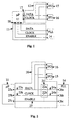
- the instruction set of circuits controlled via a separate control port differs from the instruction set of circuits controlled by addressing. Because of this, in prior art systems in which there are both circuits that are controlled by addressing and circuits controlled by a separate control port, the buses are typically separated from each other, for example like in Figure 1.
- an I 2 C bus 12 controlled by addressing connects the microprocessor 11 by means of two signal paths (DATA, CLOCK) to the first and the second I/O circuit 15 and 16, and a 3-wire bus 13 based on a separate control signal connects the microprocessor 11 by three signal paths (DATA, CLOCK, ENABLE) to the phase-locked loop 14. If many separately controlled circuits were connected to the bus 13, each one would need its own ENABLE, i.e. control, signal path.
- the I 2 C bus 12 is connected to the first I/O ports 17 of the microprocessor 11, and the 3-wire bus 13 is connected to the second I/O ports 18 of the microprocessor.
- the microprocessor can control each bus 12 and 13 separately, and the signals of one bus cannot interfere with the operation of the other bus.
- each bus type is given its own I/O port and signal path.
- the purpose of this invention is to achieve a new bus construction, which enables connecting circuits of different standards to the same path, whereby the number of the signal paths used and the number of the I/O ports used of the processor can be reduced in comparison to the prior art solution.
- the objectives are achieved by connecting the signal paths connected to the CLOCK and DATA inputs of the circuit controlled by a separate control port, such as a 3-wire circuit, via switches to the corresponding signal paths of a bus controlled by addressing, such as an I 2 C bus.
- bus construction according to the invention is characterized in what is set forth in the characterizing part of Claim 1.
- the preferred embodiments of the invention are described in the dependent claims.
- the invention has the advantage of simplifying the bus construction of the device by reducing the number of the signal paths and I/O ports of the processor in use.
- the invention provides the possibility to separate the signal paths of different buses by means of analog switches, whereby a circuit controlled by a separate control port can be disconnected from the bus construction controlled by addressing, whereby the signals directed to circuits that use addressing cannot get to the I/O ports of the circuit controlled via a separate control port.
- analog switches whereby a circuit controlled by a separate control port can be disconnected from the bus construction controlled by addressing, whereby the signals directed to circuits that use addressing cannot get to the I/O ports of the circuit controlled via a separate control port.
- Figure 2 shows an embodiment of a bus construction according to the invention.
- DATA data
- 23b CLOCK
- 27 ENABLE
- the reduction of signal paths is enabled by combining the DATA signal paths 23a and 24a and the CLOCK signal paths 23b and 24b of different bus types, respectively.
- the signal paths 23a and 23b connected to the DATA and CLOCK outputs 25a and 25b of the processor are used to transmit instructions both to circuits controlled by addressing and to circuits controlled via a separate control port 26c.
- How each circuit communicating with the microprocessor 11 is able to recognize the signals intended for it from among the signals running in the signal paths 23a; 23b and 24a; 24b depends on the standard the circuit employs.
- the circuits 15, 16 controlled by addressing recognize the signals intended for them from the commands sent by the processor 11 to the signal paths 23a and 23b, such as the START command of the I 2 C standard.
- a circuit 14 with a separate control input 26c recognizes the signals intended for it from among the signals running in the signal paths 24a and 24b by means of the ENABLE signal sent by the processor 11 via the ENABLE port 25c along the signal path 27. Having received from the signal path 27 the ENABLE signal sent by the processor 11, the circuit 14 starts to receive the signals running in the signal paths 24a and 24b, until the processor 11 sends notice that the commands coming to the circuit 14 have been executed by changing the signal to NON_ENABLE.
- the above mentioned ENABLE/NON_ENABLE signals can be implemented in a known manner, e.g. so that a certain voltage level denotes an ENABLE signal and a certain other voltage level, such as a level close to zero, denotes a NON_ENABLE signal.
- the bus construction according to the invention provides a better bit error ratio and thus also a better quality of the image, voice or data received than a combination of signal paths implemented without switches.
- the switches 22a and 22b can be advantageously implemented as analog ones, whereby the I/O ports 26a and 26b of the circuit 14 controlled via a separate control port can be analogically separated from the bus controlled by addressing. Analog separation results in a better interference protection than a digital switch configuration implemented by means of logic gates, for instance, because interference can enter the I/O ports 26a, 26b of the circuit 14 through the ground potential in a digital solution. Furthermore, using analog switches enables implementing the data transfer between the circuit 14 controlled via a separate control port 26c and the processor 11 as duplex, which would be more complicated in a digital switch construction based on logic gates, because the direction of the signal cannot be changed in logic gates.
- Switches 22a and 22b according to Figure 2 can be implemented by a switch circuit 21, such as an integrated analog switch, e.g. 74HC4053, or the switch construction can be implemented in a known manner by a FET switch composed of separate components.
- a switch circuit 21 such as an integrated analog switch, e.g. 74HC4053, or the switch construction can be implemented in a known manner by a FET switch composed of separate components.
Landscapes
- Engineering & Computer Science (AREA)
- Theoretical Computer Science (AREA)
- Physics & Mathematics (AREA)
- General Engineering & Computer Science (AREA)
- General Physics & Mathematics (AREA)
- Bus Control (AREA)
Applications Claiming Priority (2)
| Application Number | Priority Date | Filing Date | Title |
|---|---|---|---|
| FI981894 | 1998-09-04 | ||
| FI981894A FI981894A7 (fi) | 1998-09-04 | 1998-09-04 | Väylärakenne |
Publications (1)
| Publication Number | Publication Date |
|---|---|
| EP0984362A1 true EP0984362A1 (de) | 2000-03-08 |
Family
ID=8552418
Family Applications (1)
| Application Number | Title | Priority Date | Filing Date |
|---|---|---|---|
| EP99116643A Ceased EP0984362A1 (de) | 1998-09-04 | 1999-08-26 | Mehrprotokollbusverbindung |
Country Status (3)
| Country | Link |
|---|---|
| US (1) | US6397278B1 (de) |
| EP (1) | EP0984362A1 (de) |
| FI (1) | FI981894A7 (de) |
Cited By (1)
| Publication number | Priority date | Publication date | Assignee | Title |
|---|---|---|---|---|
| EP1548962A2 (de) | 2003-12-24 | 2005-06-29 | Lg Electronics Inc. | Störungsabswächende Busstruktur eines mobilen Nachrichtenendgeräts |
Families Citing this family (2)
| Publication number | Priority date | Publication date | Assignee | Title |
|---|---|---|---|---|
| DE60144025D1 (de) * | 2000-12-20 | 2011-03-24 | Thomson Licensing | I2c-bussteuerung zur isolierung ausgewählter ics für schnelle i2c-übertragung |
| US20030233507A1 (en) * | 2002-06-13 | 2003-12-18 | C-One Technology Corporation | Electronic card with multiple interfaces |
Citations (3)
| Publication number | Priority date | Publication date | Assignee | Title |
|---|---|---|---|---|
| JPS61156350A (ja) * | 1984-12-27 | 1986-07-16 | Nec Corp | 共通バス障害診断・救済方式 |
| US5376928A (en) * | 1992-09-18 | 1994-12-27 | Thomson Consumer Electronics, Inc. | Exchanging data and clock lines on multiple format data buses |
| EP0693729A1 (de) * | 1994-07-15 | 1996-01-24 | Thomson Consumer Electronics, Inc. | Mehrfachprotokoll-Datenbussystems |
Family Cites Families (6)
| Publication number | Priority date | Publication date | Assignee | Title |
|---|---|---|---|---|
| JPH05308392A (ja) | 1992-04-13 | 1993-11-19 | Sony Corp | 電子機器内の通信方式 |
| FR2707025B1 (de) * | 1993-06-21 | 1995-08-04 | Sgs Thomson Microelectronics | |
| SE504810C2 (sv) | 1995-08-22 | 1997-04-28 | Mats Iderup | Sätt och anordning vid gränssnitt,I2C/RS-232 |
| FR2740238B1 (fr) | 1995-10-19 | 1997-12-05 | Sgs Thomson Microelectronics | Cellule integrable ddc dediee a un microprocesseur |
| US6092138A (en) * | 1997-01-30 | 2000-07-18 | U.S. Philips Corporation | Electronic apparatus having a high-speed communication bus system such as an I2 C bus system |
| US5892933A (en) * | 1997-03-31 | 1999-04-06 | Compaq Computer Corp. | Digital bus |
-
1998
- 1998-09-04 FI FI981894A patent/FI981894A7/fi unknown
-
1999
- 1999-08-26 EP EP99116643A patent/EP0984362A1/de not_active Ceased
- 1999-09-03 US US09/390,589 patent/US6397278B1/en not_active Expired - Lifetime
Patent Citations (3)
| Publication number | Priority date | Publication date | Assignee | Title |
|---|---|---|---|---|
| JPS61156350A (ja) * | 1984-12-27 | 1986-07-16 | Nec Corp | 共通バス障害診断・救済方式 |
| US5376928A (en) * | 1992-09-18 | 1994-12-27 | Thomson Consumer Electronics, Inc. | Exchanging data and clock lines on multiple format data buses |
| EP0693729A1 (de) * | 1994-07-15 | 1996-01-24 | Thomson Consumer Electronics, Inc. | Mehrfachprotokoll-Datenbussystems |
Non-Patent Citations (1)
| Title |
|---|
| PATENT ABSTRACTS OF JAPAN vol. 10, no. 361 (P - 523) 4 December 1986 (1986-12-04) * |
Cited By (3)
| Publication number | Priority date | Publication date | Assignee | Title |
|---|---|---|---|---|
| EP1548962A2 (de) | 2003-12-24 | 2005-06-29 | Lg Electronics Inc. | Störungsabswächende Busstruktur eines mobilen Nachrichtenendgeräts |
| EP1548962A3 (de) * | 2003-12-24 | 2005-08-17 | Lg Electronics Inc. | Störungsabswächende Busstruktur eines mobilen Nachrichtenendgeräts |
| CN1641615B (zh) * | 2003-12-24 | 2010-05-05 | Lg电子株式会社 | 用于移动通信的噪声衰减的总线结构和方法 |
Also Published As
| Publication number | Publication date |
|---|---|
| FI981894A0 (fi) | 1998-09-04 |
| FI981894L (fi) | 2000-03-05 |
| US6397278B1 (en) | 2002-05-28 |
| FI981894A7 (fi) | 2000-03-05 |
Similar Documents
| Publication | Publication Date | Title |
|---|---|---|
| US5687330A (en) | Semiconductor process, power supply and temperature compensated system bus integrated interface architecture with precision receiver | |
| US5479123A (en) | Externally programmable integrated bus terminator for optimizing system bus performance | |
| US5657456A (en) | Semiconductor process power supply voltage and temperature compensated integrated system bus driver rise and fall time | |
| US5926514A (en) | Apparatus for clock shifting in an integrated transceiver | |
| JPH08211963A (ja) | クロックスキュー低減回路 | |
| EP1333611B1 (de) | Taktsignalerzeugungsschaltung | |
| KR19980702125A (ko) | 양방향 신호 전송 시스템 | |
| US5406147A (en) | Propagation speedup by use of complementary resolver outputs in a system bus receiver | |
| US5634014A (en) | Semiconductor process, power supply voltage and temperature compensated integrated system bus termination | |
| US6081143A (en) | Frequency comparison and generation in an integrated processor | |
| EP0984362A1 (de) | Mehrprotokollbusverbindung | |
| KR100867055B1 (ko) | 전력 전달 및 양방향 통신을 위하여 2 모드 제어된 절연회로를 구비하는 통신 장치 | |
| JPS5876938A (ja) | 異なる入出力プロトコル間の入出力デイジタル回路を構成するための装置と方法 | |
| JPH10333771A (ja) | クロック入力回路 | |
| US6124739A (en) | Monolithically integrated signal processing circuit | |
| JPH038126B2 (de) | ||
| US5036288A (en) | Circuit arrangement for clock recovery | |
| US8885694B2 (en) | Changing an operating performance point | |
| SU1562898A1 (ru) | Многоканальное устройство дл ввода-вывода информации | |
| JPS6187427A (ja) | フエ−ズロツクル−プ回路 | |
| JP3141932B2 (ja) | ネットワーク自動整合方式 | |
| US6545524B1 (en) | Configurable multiplexing circuit and method | |
| JP3045002B2 (ja) | 集積回路のモード設定回路 | |
| JPH02195719A (ja) | 集積回路 | |
| EP0157113A3 (de) | Elektronische Schnittstellenschaltung zwischen einem Rechner und einer externen Einheit |
Legal Events
| Date | Code | Title | Description |
|---|---|---|---|
| PUAI | Public reference made under article 153(3) epc to a published international application that has entered the european phase |
Free format text: ORIGINAL CODE: 0009012 |
|
| AK | Designated contracting states |
Kind code of ref document: A1 Designated state(s): DE FR GB IT |
|
| AX | Request for extension of the european patent |
Free format text: AL;LT;LV;MK;RO;SI |
|
| 17P | Request for examination filed |
Effective date: 20000211 |
|
| 17Q | First examination report despatched |
Effective date: 20000606 |
|
| AKX | Designation fees paid |
Free format text: DE FR GB IT |
|
| STAA | Information on the status of an ep patent application or granted ep patent |
Free format text: STATUS: THE APPLICATION HAS BEEN REFUSED |
|
| RAP1 | Party data changed (applicant data changed or rights of an application transferred) |
Owner name: NOKIA TECHNOLOGY GMBH |
|
| 18R | Application refused |
Effective date: 20011116 |