EP0984485B1 - Herstellungsmethode für die verdrahtung von halbleiteranordnungen - Google Patents
Herstellungsmethode für die verdrahtung von halbleiteranordnungen Download PDFInfo
- Publication number
- EP0984485B1 EP0984485B1 EP98905798A EP98905798A EP0984485B1 EP 0984485 B1 EP0984485 B1 EP 0984485B1 EP 98905798 A EP98905798 A EP 98905798A EP 98905798 A EP98905798 A EP 98905798A EP 0984485 B1 EP0984485 B1 EP 0984485B1
- Authority
- EP
- European Patent Office
- Prior art keywords
- conductor layer
- copper
- channels
- film
- wirings
- Prior art date
- Legal status (The legal status is an assumption and is not a legal conclusion. Google has not performed a legal analysis and makes no representation as to the accuracy of the status listed.)
- Expired - Lifetime
Links
Images

Classifications
-
- H—ELECTRICITY
- H10—SEMICONDUCTOR DEVICES; ELECTRIC SOLID-STATE DEVICES NOT OTHERWISE PROVIDED FOR
- H10W—GENERIC PACKAGES, INTERCONNECTIONS, CONNECTORS OR OTHER CONSTRUCTIONAL DETAILS OF DEVICES COVERED BY CLASS H10
- H10W20/00—Interconnections in chips, wafers or substrates
- H10W20/01—Manufacture or treatment
- H10W20/031—Manufacture or treatment of conductive parts of the interconnections
- H10W20/056—Manufacture or treatment of conductive parts of the interconnections by filling conductive material into holes, grooves or trenches
- H10W20/057—Manufacture or treatment of conductive parts of the interconnections by filling conductive material into holes, grooves or trenches by selectively depositing, e.g. by using selective CVD or plating
-
- H—ELECTRICITY
- H10—SEMICONDUCTOR DEVICES; ELECTRIC SOLID-STATE DEVICES NOT OTHERWISE PROVIDED FOR
- H10P—GENERIC PROCESSES OR APPARATUS FOR THE MANUFACTURE OR TREATMENT OF DEVICES COVERED BY CLASS H10
- H10P14/00—Formation of materials, e.g. in the shape of layers or pillars
- H10P14/40—Formation of materials, e.g. in the shape of layers or pillars of conductive or resistive materials
- H10P14/46—Formation of materials, e.g. in the shape of layers or pillars of conductive or resistive materials using a liquid
-
- H—ELECTRICITY
- H10—SEMICONDUCTOR DEVICES; ELECTRIC SOLID-STATE DEVICES NOT OTHERWISE PROVIDED FOR
- H10P—GENERIC PROCESSES OR APPARATUS FOR THE MANUFACTURE OR TREATMENT OF DEVICES COVERED BY CLASS H10
- H10P14/00—Formation of materials, e.g. in the shape of layers or pillars
- H10P14/40—Formation of materials, e.g. in the shape of layers or pillars of conductive or resistive materials
- H10P14/46—Formation of materials, e.g. in the shape of layers or pillars of conductive or resistive materials using a liquid
- H10P14/47—Electrolytic deposition, i.e. electroplating; Electroless plating
-
- H—ELECTRICITY
- H10—SEMICONDUCTOR DEVICES; ELECTRIC SOLID-STATE DEVICES NOT OTHERWISE PROVIDED FOR
- H10W—GENERIC PACKAGES, INTERCONNECTIONS, CONNECTORS OR OTHER CONSTRUCTIONAL DETAILS OF DEVICES COVERED BY CLASS H10
- H10W20/00—Interconnections in chips, wafers or substrates
- H10W20/40—Interconnections external to wafers or substrates, e.g. back-end-of-line [BEOL] metallisations or vias connecting to gate electrodes
- H10W20/41—Interconnections external to wafers or substrates, e.g. back-end-of-line [BEOL] metallisations or vias connecting to gate electrodes characterised by their conductive parts
- H10W20/425—Barrier, adhesion or liner layers
-
- H—ELECTRICITY
- H10—SEMICONDUCTOR DEVICES; ELECTRIC SOLID-STATE DEVICES NOT OTHERWISE PROVIDED FOR
- H10W—GENERIC PACKAGES, INTERCONNECTIONS, CONNECTORS OR OTHER CONSTRUCTIONAL DETAILS OF DEVICES COVERED BY CLASS H10
- H10W20/00—Interconnections in chips, wafers or substrates
- H10W20/40—Interconnections external to wafers or substrates, e.g. back-end-of-line [BEOL] metallisations or vias connecting to gate electrodes
- H10W20/41—Interconnections external to wafers or substrates, e.g. back-end-of-line [BEOL] metallisations or vias connecting to gate electrodes characterised by their conductive parts
- H10W20/44—Conductive materials thereof
- H10W20/4403—Conductive materials thereof based on metals, e.g. alloys, metal silicides
- H10W20/4421—Conductive materials thereof based on metals, e.g. alloys, metal silicides the principal metal being copper
-
- H—ELECTRICITY
- H10—SEMICONDUCTOR DEVICES; ELECTRIC SOLID-STATE DEVICES NOT OTHERWISE PROVIDED FOR
- H10W—GENERIC PACKAGES, INTERCONNECTIONS, CONNECTORS OR OTHER CONSTRUCTIONAL DETAILS OF DEVICES COVERED BY CLASS H10
- H10W20/00—Interconnections in chips, wafers or substrates
- H10W20/01—Manufacture or treatment
- H10W20/071—Manufacture or treatment of dielectric parts thereof
- H10W20/081—Manufacture or treatment of dielectric parts thereof by forming openings in the dielectric parts
- H10W20/084—Manufacture or treatment of dielectric parts thereof by forming openings in the dielectric parts for dual-damascene structures
Definitions
- the present invention concerns a method for forming wirings made of a metal material in connection holes or wiring grooves formed on a semiconductor substrate for conducting connections between wirings and semiconductor substrates and, more in particular, it enables complete and uniform filling of the metal material into connection holes or wiring grooves without complicating a production process.
- Wirings in integrated circuits such as LSIs have been generally formed by fabricating films of aluminum (Al) series alloys deposited by a sputtering method by using, for example, photolithography or dry etching.
- connection holes or diameters for wiring grooves apertured for conducting connection between wirings and semiconductor substrates have become finer and an aspect ratio of them has been increased more and more. Therefore, it is difficult to form wirings at a predetermined thickness as far as the inside of the connection holes by the sputtering method to result in a problem of lowering the step coverage, increasing the resistance of contact hole wirings and deteriorating electro-migration durability.
- a method of forming wirings to a vertical wiring portion in connection holes by a CVD method (chemical vapor deposition method) using tungsten (W) is adopted in LSIs under a design rule below half-micrometre.
- electrodeposition proceeds at the periphery outside of the fine connection holes or wiring grooves to at first close inlets for the connection holes or wiring grooves, which causes a problem of difficulty for filing copper in the fine connection holes without forming voids.
- connection hole or wiring grooves it is difficult to fabricate copper by dry etching and it has been proposed, for example, a DUAL DAMASCENE method of forming contact holes and wiring grooves to an insulation film, depositing copper for the entire surface and then removing excess copper by a chemical and mechanical polishing method thereby properly forming wirings having vertical connection portions.
- Development for the technique of properly filling and depositing a copper film into hole or groove portions of high aspect ratio such as connection hole or wiring grooves has also been desired with an aim of applying to this method.
- the present invention has been accomplished taking notice of the foregoing not yet solved problem. It is an object of the invention to provide a selective plating method capable of completely, and uniformly filling groove or hole portions of high aspect ratio and a wiring forming method for a semiconductor device using the same.
- the present invention provides a method of forming wirings for a semiconductor device, which comprises the steps of providing a semiconductor substrate having an insulation film formed thereon; forming channels having an aspect ratio from 1 to 5 and a width of 1.0 ⁇ m or less in the insulation film, forming a first conductor layer by a CVD process on the surface of the insulation film including the inner surface of the channels, then forming a second conductor layer by a sputtering process on the surface of the first conductor layer except for the inner surface the channels, the first conductor layer and the second conductor layer having respective surface potentials such that the voltage for depositing a copper series metal from a plating solution on to the second conductor layer - the second overvoltage - is higher than the voltage for depositing a copper series metal from a plating solution on to the first conductor layer - the first overvoltage); subsequently, dipping at least the channels into the plating solution and applying a plating treatment at a voltage higher than the first overvoltage and
- the first conductor layer having a first deposition voltage is formed on the inner surface of the wiring channels such as connection holes or wiring grooves formed in the insulation film deposited on the semiconductor substrate by a CVD method, and then the second conductor layer having a second deposition voltage is formed thereon so as to cover the surface of the first conductor layer except for the inner surface of the channels by a sputtering method. Then, they are dipped in the plating solution such that at least the channels are immersed in the plating solution, and a plating treatment is applied at a deposition voltage higher than the first voltage and lower than the second voltage.
- the deposition voltage is a voltage required for depositing the copper series metal material in the plating solution at a predetermined rate
- the metal material is not deposited on a portion in which the second conductor layer is exposed, whereas chemical reactions are taken place between the metal material in the plating solution and the first conductor layer to deposit the metal material and apply copper plating to the portion in which the first conductor layer is exposed. That is, since copper plating is applied only to the portion in which the first conductor layer is exposed, namely, only to the inner surface of the channels intended to be applied with plating, to result in a copper-filled state, a wiring consisting of copper filled in the channels can be obtained by polishing the copper.
- the second conductor layer is formed by a highly anisotropic deposition method. This is done for forming the second conductor layer to a region except for a region to be plated, namely, only to a region except for the inner surface of the channels and the formation of the second conductor layer in the wiring channels is avoided.
- each wiring channel has an aspect ratio of 1 or greater and 5 or less and a width of 1.0 ⁇ m or less. This is so defined for avoiding the formation of the second conductor layer on the inner surface of the channels upon forming the second conductor layer by a sputtering method.
- plating is applied to form wirings and then wirings are conducted by forming a metal film further thereon.
- a thin electrically conductive film is generally put between them with an aim, for example, of improving adhesion and electro-migration durability.
- the step of forming wirings can be shortened by utilizing the layer as the thin electrically conductive film.
- the deposited metal material is preferably polished by a chemical and mechanical polishing method by which the wirings can be formed easily and accurately.
- copper wirings uniformly filled in the channels can be formed by forming a titanium nitride film to the inner surface of the channels such as connection holes or wiring grooves, forming a titanium film so as to cover the surface of the titanium nitride film except for the wiring channels and then dipping them into a plating solution.
- an electrode potential is set to a potential which is negative by an overvoltage than a thermodynamic equilibrium potential required for reducing to deposit metal ions in the plating solution.
- a reducing agent having a reducing power (oxidation/reduction potential) higher than an equilibrium potential required for depositing metal ions is used.
- Deposition by reduction of metal ions does not proceed at a substantial rate even when the thermodynamic equilibrium electrode potential or an oxidant providing the oxidation/reduction potential is used; an overvoltage is required for a substantial reaction to proceed, which is different depending on the kind of the underlying metal. That is, there is a phenomenon that an electrode potential or oxidation/reduction potential of the reducing agent (hereinafter referred to as a deposition overvoltage) in excess of the thermodynamical equilibrium potential is required and is different depending on the kind of the underlying metal.
- a deposition overvoltage an electrode potential or oxidation/reduction potential of the reducing agent in excess of the thermodynamical equilibrium potential is required and is different depending on the kind of the underlying metal.
- a first underlying metal having a lower deposition overvoltage as the first deposition overvoltage is selected and deposited as a film on a portion to be deposited with copper
- a second underlying metal having a deposition overvoltage higher than the first deposition overvoltage as a second deposition overvoltage is selected and deposited as a film to a portion not intended to be deposited with copper
- a voltage higher than the first deposition overvoltage and lower than the second deposition overvoltage is set as an electrode potential relative to a counter-electrode in a case of electrolytic plating
- a oxidation/reduction potential of a reducing agent is set higher than the first deposition overvoltage and lower than the second deposition overvoltage in a case of electroless plating.
- copper is deposited to form a metal film only to a portion in which the first underlying metal is exposed. Accordingly, plating is conducted till copper is deposited as far as the upper surface of the wiring grooves and the connection holes, to provide a state in which a metal film of the deposited copper is filled in the wiring grooves and the contact holes. Accordingly, wirings of copper filled in the wiring grooves and the connection holes can be obtained by polishing the deposited copper by a chemical and mechanical polishing method to remove unnecessary portion.
- dense thin electrically conductive films such as of titanium nitride (TiN) are formed generally at the boundary between the insulation film and the wirings with various purposes such as prevention of diffusion, improvement of adhesion and improvement of electro-migration durability. Since such films have higher resistance compared with aluminum or copper, it is not preferred to make them unnecessarily thick.
- electric current can be supplied through the underlying metal such as titanium nitride formed as a film on the entire surface of the insulation film.
- titanium nitride is used as the first underlying metal having the first deposition overvoltage as the deposition overvoltage and deposited as a film on the entire surface of the insulation film, and then a film of metal such as titanium having a high deposition overvoltage is formed thinly by a highly anisotropic deposition method being sputtering to a portion not intended to apply plating, namely, a region except for the side wall and the bottom of the connection holes and the wiring grooves, a copper film is not formed to the titanium deposited portion and copper can be deposited substantially only to the portion not deposited with titanium, namely, only to the side wall and the bottom of the connection holes and the wiring grooves.
- the titanium nitride film can be utilized as the thin electrically conductive film for the improvement of the adhesion and improvement of the electro-migration durability, so that it is not necessary to form an additional thin electrically conductive film, for example, in a case of applying wirings in the multi-layered wiring structure, and the wiring forming step can be saved.
- the second underlying metal having the second deposited overvoltage as the deposition overvoltage is deposited as a film by the sputtering method, but the metal of high deposition overvoltage adheres to the bottom of the wiring grooves and the connection holes if the width of the wiring grooves and the diameter of the connection holes are large. Therefore, the width of the grooves and the diameter of the connection holes are 1.0 ⁇ m or less, and the aspect ratio as the width to depth ratio in the wiring grooves and the connection holes is from 1 to 5. If necessary, preferred deposition can be applied by providing a cleaning step before electrodeposition by electrolytic plating.
- the metal film of copper is formed so as to fill the wiring grooves and the like by applying plating described above, voids are not formed in the metal film and a uniform copper film can be obtained.
- wirings can be formed effectively even in fine wiring grooves or connection holes and, in addition, copper having high electro-migration durability and low resistance can be used as the wiring material, so that the method can be applied even to fine wiring grooves or suitable to connection holes and it is preferred in a case of forming fine wirings such as the connection portions between a silicon substrate and wirings, or between wiring layers in a multi-layered wiring structure. Furthermore, since fine wirings can be formed, the size of the semiconductor substrate can be reduced.
- the conductors of different deposition overvoltages can be easily determined experimentally in accordance with the kind of metal to be deposited.
- the metal to be deposited is copper, copper (CU), zinc (Zn) or gold (Au) can be used for the conductor of low deposition overvoltage and, on the other hand, iron (Fe), nickel (Ni), cobalt (Co), titanium (Ti) and tungsten (W) can be used for the conductor of high deposition overvoltage.
- optional materials may be selected.
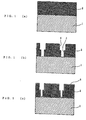
- a 15 cm (6 inch) substrate 1 of n-type Si (100) single crystal having a resistance of 2 ⁇ cm was used as a semiconductor substrate and a silicon oxide insulation film 2 was formed to a thickness of 2.0 ⁇ m on the substrate by a plasma CVD method.
- connection hole 3 and a wiring groove 4 were formed in the silicon oxide insulation film 2 by using a photolithographic method and a dry etching method (Fig. 1 (b)).
- the connection hole 3 had a 0.6 ⁇ m diameter and a 1.0 ⁇ m depth and the wiring groove 4 had a 0.8 ⁇ m width and a 1.0 ⁇ m depth.
- the connection hole 3 and the wiring groove 4 correspond to the wiring channel.
- a titanium nitride film (first conductor layer) 5 having a deposition overvoltage of about -100 mV was deposited to a thickness of 0.1 ⁇ m over the entire surface of the semiconductor substrate 1 by a CVD method (Fig. 1(c)).
- the deposition overvoltage of titanium nitride is a value based on a saturation calomel electrode.
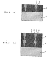
- titanium (second conductor layer) 6 having a deposition overvoltage of about -300 mV was sputtered to a thickness of 0.03 ⁇ m on a flat surface, that is, a portion except for the connection hole 3 and the wiring groove 4 (Fig. 2(a)).
- a usual sputtering method, a sputtering method using a collimator, a long distance sputtering method or the like is adopted.
- the deposition overvoltage of titanium is a value based on the saturation calomel electrode.
- the specimen material to be plated
- the specimen was subjected to constant current electrolysis in a plating solution using copper sulfate (cupric metal material) using a copper electrode as a counter electrode, at a current of 50 mA for 10 min.
- the potential difference between both of the electrodes was about 200 mV.
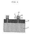
- the specimen may also be polished by using the chemical and mechanical polishing method to remove excessively deposited copper, titanium and titanium nitride as shown in Fig. 3(a) and, subsequently, applying molding, for example.
- the silicon oxide insulation film 8 is formed again and, subsequently, a connection hole 9 and a wiring groove 10 are formed in the silicon oxide insulation film 8 as shown in Fig. 3(b) by repeating the procedures described above. Then, after depositing a titanium nitride film 11 to the entire surface of the specimen, a titanium film is deposited to a portion except for the connection hole 9 and the wiring groove 10, then plating is applied under the same conditions as described above, excess copper and the like are removed by polishing, thereby forming wirings 12 in the connection hole 9 and the wiring groove 10 to form multi-layered wiring.
- a titanium nitride film 14 is deposited on the entire surface of the specimen, further, a titanium film 15 is formed to a region except for the connection hole 3, and then plating is applied to form wirings 7 in the connection hole 3 by deposition of copper. Then, excess copper is removed by polishing, a wiring film 17 is deposited further thereon, and the wiring film 17, the titanium film 15 and the titanium nitride film 14 are patterned together to form wirings.
- an electrically conductive thin film is generally put between them with an aim of improving the adhesion and improving the electro-migration durability.
- the titanium nitride film 14 and the titanium film 15 are left upon polishing the deposited copper and the wiring film 17 is deposited on the titanium film 15, so that the titanium nitride film 14 can be utilized as the thin electrically conductive film to shorten the step of forming the wirings.
Landscapes
- Internal Circuitry In Semiconductor Integrated Circuit Devices (AREA)
- Electrodes Of Semiconductors (AREA)
Claims (3)
- Verfahren zum Bilden von Verdrahtungen für eine Halbleitervorrichtung, das die Schritte umfasst:wobei die erste Leiterschicht (5) und die zweite Leiterschicht (6) jeweilige Oberflächenpotenziale aufweisen, die.derart sind, dass die Spannung zum Abscheiden eines Metalls der Kupferreihe aus einer Plattierungslösung auf der zweiten Leiterschicht die zweite Überspannung - höher ist als die Spannung zum Abscheiden eines Metalls der Kupferreihe aus einer Plattierungslösung auf der ersten Leiterschicht - die erste Überspannung,Bereitstellen eines Halbleitersubstrats (1) mit einem darauf ausgebildeten Isolierfilm (2), Bilden von Kanälen (4) mit einem Seitenverhältnis von 1 bis 5 und einer Breite von 1,0 µm oder weniger in dem Isolierfilm (2),Bilden einer ersten Leiterschicht (5) mit einem CVD-Verfahren auf der Oberfläche des Isolierfilms, einschließlich der Innenoberfläche der Kanäle (4),anschließend Bilden einer zweiten Leiterschicht durch ein Sputterverfahren auf der Oberfläche der ersten Leiterschicht (5), mit Ausnahme der Innenoberfläche der Kanäle (4),
anschließend Eintauchen mindestens der Kanäle (4) in die Plattierungslösung und Durchführen einer Plattierungsbehandlung bei einer Spannung, die höher ist als die erste Überspannung und niedriger ist als die zweite Überspannung, zum Abscheiden des Metallmaterials der Kupferreihe auf der Innenoberfläche der Kanäle (4), und
Polieren des abgeschiedenen Metallmaterials der Kupferreihe zur Entfernung nicht erforderlicher Abschnitte, wodurch das abgeschiedene Metall der Kupferreihe Verdrahtungen bildet, die sich in den Kanälen (4) befinden. - Verfahren nach Anspruch 1, das auf eine Halbleitervorrichtung mit einer mehrschichtigen Verdrahtungsstruktur angewandt wird.
- Verfahren nach Anspruch 1 oder 2, bei dem die erste Leiterschicht (5) aus Titannitrid, die zweite Leiterschicht (6) aus Titan und das Metallmaterial (7) aus einem Metallmaterial der Kupferreihe hergestellt ist.
Priority Applications (1)
| Application Number | Priority Date | Filing Date | Title |
|---|---|---|---|
| EP04078198A EP1533837A1 (de) | 1997-03-10 | 1998-03-06 | Verfahren zum selektiven Galvanisieren |
Applications Claiming Priority (3)
| Application Number | Priority Date | Filing Date | Title |
|---|---|---|---|
| JP5459397 | 1997-03-10 | ||
| JP5459397 | 1997-03-10 | ||
| PCT/JP1998/000939 WO1998040910A1 (fr) | 1997-03-10 | 1998-03-06 | Procede pour former le cablage dans un dispositif a semi-conducteur, et dispositif a semi-conducteur |
Related Child Applications (1)
| Application Number | Title | Priority Date | Filing Date |
|---|---|---|---|
| EP04078198.1 Division-Into | 2004-11-24 |
Publications (3)
| Publication Number | Publication Date |
|---|---|
| EP0984485A1 EP0984485A1 (de) | 2000-03-08 |
| EP0984485A4 EP0984485A4 (de) | 2001-05-23 |
| EP0984485B1 true EP0984485B1 (de) | 2005-11-16 |
Family
ID=12975034
Family Applications (2)
| Application Number | Title | Priority Date | Filing Date |
|---|---|---|---|
| EP98905798A Expired - Lifetime EP0984485B1 (de) | 1997-03-10 | 1998-03-06 | Herstellungsmethode für die verdrahtung von halbleiteranordnungen |
| EP04078198A Withdrawn EP1533837A1 (de) | 1997-03-10 | 1998-03-06 | Verfahren zum selektiven Galvanisieren |
Family Applications After (1)
| Application Number | Title | Priority Date | Filing Date |
|---|---|---|---|
| EP04078198A Withdrawn EP1533837A1 (de) | 1997-03-10 | 1998-03-06 | Verfahren zum selektiven Galvanisieren |
Country Status (8)
| Country | Link |
|---|---|
| US (2) | US6384484B1 (de) |
| EP (2) | EP0984485B1 (de) |
| JP (1) | JP4297292B2 (de) |
| KR (1) | KR20000076081A (de) |
| CN (1) | CN1250545A (de) |
| AU (1) | AU6120898A (de) |
| DE (1) | DE69832380T2 (de) |
| WO (1) | WO1998040910A1 (de) |
Families Citing this family (14)
| Publication number | Priority date | Publication date | Assignee | Title |
|---|---|---|---|---|
| JP3694594B2 (ja) * | 1998-09-03 | 2005-09-14 | 株式会社荏原製作所 | 微細孔および/または微細溝を有する基材の孔埋めめっき方法 |
| US6610126B2 (en) | 2001-06-06 | 2003-08-26 | Donaldson Company, Inc. | Filter element having sealing members and methods |
| KR100440471B1 (ko) * | 2002-10-02 | 2004-07-14 | 아남반도체 주식회사 | 반도체 소자 제조 방법 |
| US7238610B2 (en) * | 2003-03-31 | 2007-07-03 | Intel Corporation | Method and apparatus for selective deposition |
| JP2004353004A (ja) * | 2003-05-27 | 2004-12-16 | Ebara Corp | めっき装置 |
| US20080261400A1 (en) * | 2005-12-21 | 2008-10-23 | Asahi Glass Company, Limited | Polishing composition, polishing method, and method for forming copper wiring for semiconductor integrated circuit |
| US7989347B2 (en) * | 2006-03-30 | 2011-08-02 | Freescale Semiconductor, Inc. | Process for filling recessed features in a dielectric substrate |
| CN100419514C (zh) * | 2006-10-13 | 2008-09-17 | 友达光电股份有限公司 | 液晶显示器用基板的制作方法 |
| DE102006062189B4 (de) | 2006-12-22 | 2009-03-19 | Dr. Mirtsch Gmbh | Verfahren zum Herstellen einer strukturierten Materialbahn für das Durchströmen von fluiden Medien, strukturierte Materialbahn und Verwendung derselben |
| US8764961B2 (en) | 2008-01-15 | 2014-07-01 | Applied Materials, Inc. | Cu surface plasma treatment to improve gapfill window |
| JP5498751B2 (ja) * | 2009-10-05 | 2014-05-21 | ルネサスエレクトロニクス株式会社 | 半導体装置の製造方法 |
| JP2011096705A (ja) * | 2009-10-27 | 2011-05-12 | Fujitsu Ltd | 基板製造方法及び基板 |
| CN103219278A (zh) * | 2012-01-19 | 2013-07-24 | 刘胜 | 硅圆片通孔金属填充工艺 |
| DE102013002213B4 (de) | 2013-02-07 | 2016-06-02 | Dr. Mirtsch Gmbh | Verfahren zum Herstellen einer strukturierten Materialbahn aus gewirkten, gestrickten oder gewebten Fäden und Verwendung derselben |
Family Cites Families (13)
| Publication number | Priority date | Publication date | Assignee | Title |
|---|---|---|---|---|
| GB1175667A (en) * | 1966-04-07 | 1969-12-23 | Associated Semiconductor Mft | Improvements in the Electrodeposition of Metals using a Composite Mask |
| SE446751B (sv) * | 1974-02-19 | 1986-10-06 | Western Electric Co | Forfarande for selektiv elektropletering av mjukt guld pa ett edelmetallomrade |
| JPS59205735A (ja) * | 1983-05-09 | 1984-11-21 | Nec Corp | 半導体装置の製造方法 |
| US4988412A (en) * | 1988-12-27 | 1991-01-29 | General Electric Company | Selective electrolytic desposition on conductive and non-conductive substrates |
| US5188723A (en) * | 1992-04-13 | 1993-02-23 | Micron Technology, Inc. | Selective electro-deposition and circuit patterning technique |
| JPH0799199A (ja) * | 1993-06-03 | 1995-04-11 | Nec Corp | 半導体装置の製造方法 |
| JPH07283219A (ja) * | 1994-04-13 | 1995-10-27 | Sanyo Electric Co Ltd | 半導体装置および半導体装置の製造方法および半導体装 置の製造装置 |
| US5602423A (en) | 1994-11-01 | 1997-02-11 | Texas Instruments Incorporated | Damascene conductors with embedded pillars |
| KR0144913B1 (ko) * | 1995-03-03 | 1998-08-17 | 김광호 | 반도체장치의 금속배선층 형성방법 |
| US5676587A (en) * | 1995-12-06 | 1997-10-14 | International Business Machines Corporation | Selective polish process for titanium, titanium nitride, tantalum and tantalum nitride |
| US5824599A (en) * | 1996-01-16 | 1998-10-20 | Cornell Research Foundation, Inc. | Protected encapsulation of catalytic layer for electroless copper interconnect |
| US5702982A (en) * | 1996-03-28 | 1997-12-30 | Taiwan Semiconductor Manufacturing Company, Ltd. | Method for making metal contacts and interconnections concurrently on semiconductor integrated circuits |
| US5968333A (en) * | 1998-04-07 | 1999-10-19 | Advanced Micro Devices, Inc. | Method of electroplating a copper or copper alloy interconnect |
-
1998
- 1998-03-06 EP EP98905798A patent/EP0984485B1/de not_active Expired - Lifetime
- 1998-03-06 KR KR1019997008169A patent/KR20000076081A/ko not_active Abandoned
- 1998-03-06 DE DE69832380T patent/DE69832380T2/de not_active Expired - Lifetime
- 1998-03-06 CN CN98803281A patent/CN1250545A/zh active Pending
- 1998-03-06 EP EP04078198A patent/EP1533837A1/de not_active Withdrawn
- 1998-03-06 AU AU61208/98A patent/AU6120898A/en not_active Abandoned
- 1998-03-06 JP JP53942598A patent/JP4297292B2/ja not_active Expired - Fee Related
- 1998-03-06 WO PCT/JP1998/000939 patent/WO1998040910A1/ja not_active Ceased
- 1998-03-06 US US09/380,780 patent/US6384484B1/en not_active Expired - Lifetime
-
2002
- 2002-04-04 US US10/115,252 patent/US6541379B2/en not_active Expired - Lifetime
Also Published As
| Publication number | Publication date |
|---|---|
| DE69832380T2 (de) | 2006-08-03 |
| US20020105090A1 (en) | 2002-08-08 |
| US6384484B1 (en) | 2002-05-07 |
| US6541379B2 (en) | 2003-04-01 |
| WO1998040910A1 (fr) | 1998-09-17 |
| JP4297292B2 (ja) | 2009-07-15 |
| EP0984485A4 (de) | 2001-05-23 |
| EP0984485A1 (de) | 2000-03-08 |
| KR20000076081A (ko) | 2000-12-26 |
| DE69832380D1 (de) | 2005-12-22 |
| CN1250545A (zh) | 2000-04-12 |
| EP1533837A1 (de) | 2005-05-25 |
| AU6120898A (en) | 1998-09-29 |
Similar Documents
| Publication | Publication Date | Title |
|---|---|---|
| JP3116897B2 (ja) | 微細配線形成方法 | |
| KR100332185B1 (ko) | 전기도금방법,금속피쳐패턴제공방법,전극패턴제공방법,금속화패턴제공방법,패터닝된도전성구조체,커패시터구조체 | |
| US8012875B2 (en) | Method and apparatus for workpiece surface modification for selective material deposition | |
| US6946066B2 (en) | Multi step electrodeposition process for reducing defects and minimizing film thickness | |
| US6420258B1 (en) | Selective growth of copper for advanced metallization | |
| US8058164B2 (en) | Methods of fabricating electronic devices using direct copper plating | |
| US20040219779A1 (en) | Method and structure to improve reliability of copper interconnects | |
| US6384484B1 (en) | Semiconductor device | |
| US7704880B1 (en) | Method of forming contact layers on substrates | |
| JP2001185553A (ja) | 電気めっき充填を改善する方法 | |
| JPH07283219A (ja) | 半導体装置および半導体装置の製造方法および半導体装 置の製造装置 | |
| JPWO1998040910A1 (ja) | 半導体装置の配線形成方法及び半導体装置 | |
| JP2013524019A (ja) | ミクロスケール構造中でのシード層堆積 | |
| US20040229462A1 (en) | Method to reduce the copper line roughness for increased electrical conductivity of narrow interconnects (<100nm) | |
| TWI270112B (en) | Reverse-tone mask method for post-CMP elimination of copper overburden humps | |
| KR100572825B1 (ko) | 반도체 소자의 금속배선 형성방법 | |
| JP2000031145A (ja) | 半導体装置の製造方法 | |
| US6797144B2 (en) | Method for reducing surface defects in an electrodeposition process | |
| JP2005079156A (ja) | 配線形成方法 | |
| US20040217013A1 (en) | Apparatus and method for electropolishing a metal wiring layer on a semiconductor device | |
| US7597787B2 (en) | Methods and apparatuses for electrochemical deposition | |
| KR20090072215A (ko) | 반도체 소자의 제조 방법 |
Legal Events
| Date | Code | Title | Description |
|---|---|---|---|
| PUAI | Public reference made under article 153(3) epc to a published international application that has entered the european phase |
Free format text: ORIGINAL CODE: 0009012 |
|
| 17P | Request for examination filed |
Effective date: 19990916 |
|
| AK | Designated contracting states |
Kind code of ref document: A1 Designated state(s): DE FR GB |
|
| A4 | Supplementary search report drawn up and despatched |
Effective date: 20010406 |
|
| AK | Designated contracting states |
Kind code of ref document: A4 Designated state(s): DE FR GB |
|
| RAP1 | Party data changed (applicant data changed or rights of an application transferred) |
Owner name: ASAHI KASEI KABUSHIKI KAISHA |
|
| 17Q | First examination report despatched |
Effective date: 20030718 |
|
| GRAP | Despatch of communication of intention to grant a patent |
Free format text: ORIGINAL CODE: EPIDOSNIGR1 |
|
| RTI1 | Title (correction) |
Free format text: WIRING FORMING METHOD FOR SEMICONDUCTOR DEVICE |
|
| GRAS | Grant fee paid |
Free format text: ORIGINAL CODE: EPIDOSNIGR3 |
|
| GRAA | (expected) grant |
Free format text: ORIGINAL CODE: 0009210 |
|
| AK | Designated contracting states |
Kind code of ref document: B1 Designated state(s): DE FR GB |
|
| REG | Reference to a national code |
Ref country code: GB Ref legal event code: FG4D |
|
| REF | Corresponds to: |
Ref document number: 69832380 Country of ref document: DE Date of ref document: 20051222 Kind code of ref document: P |
|
| ET | Fr: translation filed | ||
| PLBE | No opposition filed within time limit |
Free format text: ORIGINAL CODE: 0009261 |
|
| STAA | Information on the status of an ep patent application or granted ep patent |
Free format text: STATUS: NO OPPOSITION FILED WITHIN TIME LIMIT |
|
| 26N | No opposition filed |
Effective date: 20060817 |
|
| REG | Reference to a national code |
Ref country code: FR Ref legal event code: PLFP Year of fee payment: 18 |
|
| PGFP | Annual fee paid to national office [announced via postgrant information from national office to epo] |
Ref country code: DE Payment date: 20150305 Year of fee payment: 18 |
|
| PGFP | Annual fee paid to national office [announced via postgrant information from national office to epo] |
Ref country code: FR Payment date: 20150309 Year of fee payment: 18 Ref country code: GB Payment date: 20150304 Year of fee payment: 18 |
|
| REG | Reference to a national code |
Ref country code: DE Ref legal event code: R119 Ref document number: 69832380 Country of ref document: DE |
|
| GBPC | Gb: european patent ceased through non-payment of renewal fee |
Effective date: 20160306 |
|
| REG | Reference to a national code |
Ref country code: FR Ref legal event code: ST Effective date: 20161130 |
|
| PG25 | Lapsed in a contracting state [announced via postgrant information from national office to epo] |
Ref country code: GB Free format text: LAPSE BECAUSE OF NON-PAYMENT OF DUE FEES Effective date: 20160306 Ref country code: FR Free format text: LAPSE BECAUSE OF NON-PAYMENT OF DUE FEES Effective date: 20160331 Ref country code: DE Free format text: LAPSE BECAUSE OF NON-PAYMENT OF DUE FEES Effective date: 20161001 |