EP0984487A2 - Methode zur Herstellung einer MOSFET-Struktur mit flacher Wanne - Google Patents
Methode zur Herstellung einer MOSFET-Struktur mit flacher Wanne Download PDFInfo
- Publication number
- EP0984487A2 EP0984487A2 EP99115841A EP99115841A EP0984487A2 EP 0984487 A2 EP0984487 A2 EP 0984487A2 EP 99115841 A EP99115841 A EP 99115841A EP 99115841 A EP99115841 A EP 99115841A EP 0984487 A2 EP0984487 A2 EP 0984487A2
- Authority
- EP
- European Patent Office
- Prior art keywords
- layer
- conductivity type
- surface layer
- thickness
- gate
- Prior art date
- Legal status (The legal status is an assumption and is not a legal conclusion. Google has not performed a legal analysis and makes no representation as to the accuracy of the status listed.)
- Withdrawn
Links
- 238000004519 manufacturing process Methods 0.000 title claims description 7
- 239000012212 insulator Substances 0.000 claims abstract description 69
- 125000006850 spacer group Chemical group 0.000 claims abstract description 43
- 239000012535 impurity Substances 0.000 claims abstract description 31
- 239000010410 layer Substances 0.000 claims description 179
- 239000002344 surface layer Substances 0.000 claims description 64
- 239000000463 material Substances 0.000 claims description 50
- 239000004065 semiconductor Substances 0.000 claims description 22
- 239000000758 substrate Substances 0.000 claims description 19
- 238000000034 method Methods 0.000 claims description 17
- 230000005669 field effect Effects 0.000 claims description 8
- 238000005530 etching Methods 0.000 claims description 4
- 229910021420 polycrystalline silicon Inorganic materials 0.000 abstract description 30
- 239000007943 implant Substances 0.000 abstract description 27
- 229920005591 polysilicon Polymers 0.000 abstract description 25
- 108091006146 Channels Proteins 0.000 description 26
- 230000015572 biosynthetic process Effects 0.000 description 11
- 239000002019 doping agent Substances 0.000 description 10
- 238000009792 diffusion process Methods 0.000 description 7
- 229910052710 silicon Inorganic materials 0.000 description 6
- 239000010703 silicon Substances 0.000 description 6
- XUIMIQQOPSSXEZ-UHFFFAOYSA-N Silicon Chemical compound [Si] XUIMIQQOPSSXEZ-UHFFFAOYSA-N 0.000 description 4
- 230000015556 catabolic process Effects 0.000 description 4
- 230000000694 effects Effects 0.000 description 4
- 230000035515 penetration Effects 0.000 description 4
- 150000001875 compounds Chemical class 0.000 description 3
- 230000003247 decreasing effect Effects 0.000 description 3
- 230000008021 deposition Effects 0.000 description 3
- 229920002120 photoresistant polymer Polymers 0.000 description 3
- 108010075750 P-Type Calcium Channels Proteins 0.000 description 2
- 230000004913 activation Effects 0.000 description 2
- 210000000746 body region Anatomy 0.000 description 2
- 230000000903 blocking effect Effects 0.000 description 1
- 239000002800 charge carrier Substances 0.000 description 1
- 230000001419 dependent effect Effects 0.000 description 1
- 230000002028 premature Effects 0.000 description 1
Images


Classifications
-
- H—ELECTRICITY
- H10—SEMICONDUCTOR DEVICES; ELECTRIC SOLID-STATE DEVICES NOT OTHERWISE PROVIDED FOR
- H10D—INORGANIC ELECTRIC SEMICONDUCTOR DEVICES
- H10D30/00—Field-effect transistors [FET]
- H10D30/60—Insulated-gate field-effect transistors [IGFET]
- H10D30/64—Double-diffused metal-oxide semiconductor [DMOS] FETs
- H10D30/66—Vertical DMOS [VDMOS] FETs
-
- H—ELECTRICITY
- H10—SEMICONDUCTOR DEVICES; ELECTRIC SOLID-STATE DEVICES NOT OTHERWISE PROVIDED FOR
- H10D—INORGANIC ELECTRIC SEMICONDUCTOR DEVICES
- H10D30/00—Field-effect transistors [FET]
- H10D30/01—Manufacture or treatment
- H10D30/021—Manufacture or treatment of FETs having insulated gates [IGFET]
- H10D30/028—Manufacture or treatment of FETs having insulated gates [IGFET] of double-diffused metal oxide semiconductor [DMOS] FETs
- H10D30/0291—Manufacture or treatment of FETs having insulated gates [IGFET] of double-diffused metal oxide semiconductor [DMOS] FETs of vertical DMOS [VDMOS] FETs
-
- H—ELECTRICITY
- H10—SEMICONDUCTOR DEVICES; ELECTRIC SOLID-STATE DEVICES NOT OTHERWISE PROVIDED FOR
- H10D—INORGANIC ELECTRIC SEMICONDUCTOR DEVICES
- H10D30/00—Field-effect transistors [FET]
- H10D30/60—Insulated-gate field-effect transistors [IGFET]
- H10D30/64—Double-diffused metal-oxide semiconductor [DMOS] FETs
- H10D30/66—Vertical DMOS [VDMOS] FETs
- H10D30/662—Vertical DMOS [VDMOS] FETs having a drift region having a doping concentration that is higher between adjacent body regions relative to other parts of the drift region
-
- H—ELECTRICITY
- H10—SEMICONDUCTOR DEVICES; ELECTRIC SOLID-STATE DEVICES NOT OTHERWISE PROVIDED FOR
- H10D—INORGANIC ELECTRIC SEMICONDUCTOR DEVICES
- H10D62/00—Semiconductor bodies, or regions thereof, of devices having potential barriers
- H10D62/10—Shapes, relative sizes or dispositions of the regions of the semiconductor bodies; Shapes of the semiconductor bodies
- H10D62/13—Semiconductor regions connected to electrodes carrying current to be rectified, amplified or switched, e.g. source or drain regions
- H10D62/149—Source or drain regions of field-effect devices
- H10D62/151—Source or drain regions of field-effect devices of IGFETs
Definitions
- the present invention relates to semiconductor devices and processes for their manufacture, and is particularly directed to a process for manufacturing a shallow well insulated gate field effect semiconductor device, and a device made by that process, having decreased resistance and current pinching in the neck region of the channel.
- the well depth required for achieving a desired channel length is dependent upon or dictated by lateral and vertical diffusion of dopant material beneath the edge of a polysilicon gate.
- the device being formed is intended to be a reduced depth or shallow well device, such a diffusion dependency tends to make the resulting device prone to short channel effects and high drain-source leakage.
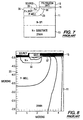
- an N-epitaxial layer 11 is initially ubiquitously deposited upon an underlying N+ silicon substrate 13 ( Figure 1), to a prescribed thickness and resistivity for achieving a prescribed breakdown voltage.
- a gate insulator (oxide) layer 15 is grown on the top surface of the N- epitaxial layer 11 ( Figure 2), followed by non-selective deposition of a layer 19 of polycrystalline silicon ( Figure 3), which is to serve as the gate electrode for the device.
- the gate oxide 15 and polysilicon layer 19 are then selectively etched ( Figure 4) to define a self-aligned mask 21 for subsequent well and source implants.
- a P-well region 25 is then formed in the epitaxial layer 11 by means of a blanket or non-selective implant of P-type impurities 23, having an energy and concentration that produces the P-well region 25 adjacent to the side edge 27 of the gate mask 21.
- This structure is then subjected to a drive-in diffusion/anneal, which increases the depth of the P-well region 25 and causes lateral diffusion of the implanted P-well impurities beneath the gate mask 21, so that a resulting PN junction 27, between the P-well region 25 and the N-epitaxial layer 11, extends from the bottom 29 of the well P-region to a location 31 beneath the insulated gate structure.
- an N+ source region 33 is selectively implanted into the well adjacent to the side edge 27 of the gate, using a separate photoresist mask and an oxide spacer or photoresist mask overlying the P-well region 25, to define the size of the source region.
- An area 50 directly below the gate oxide 15 and located between the N+ source region 33 and drain 11, 13 is now formed and defined as a channel area.
- a further P+ implant is carried out, to form a surface P+ body region 35 within the P-well region 25 ( Figure 7).
- the structure is then annealed for dopant activation and repair of damaged lattice sites. In the final device, the back side of the substrate will serve as a drain contact.
- Figure 8 diagrammatically illustrates the concentration of current flow during the on-state of a device manufactured using the conventional processing sequence of Figures 1-7.
- the length of the channel 50 is determined by lateral and vertical diffusion of dopant material beneath the side edge 27 of the gate structure, at the location of the well implant to form a relatively shallow well device (less than two microns in the illustrated example), the resulting device is prone to short channel effects and high drain-source leakage and in extreme cases breakdown voltage reduction.
- the short channel effects are evident when the device is in conduction or on-state.
- charge carriers flow through the channel region between the source and drain regions under the control of the voltage applied to the gate electrode relative to the voltage applied to the source region.
- a positive voltage is applied to the gate electrode 19 for attracting electrons toward the surface of the channel region.
- the attracted electrons when of sufficient concentration, invert the conductivity type of a narrow portion of the P-type channel region adjacent to the substrate surface to N-type for establishing a continuous path of N-type conductivity from the source region 33 through the channel region 50 to the drain region 11 and 13 down to the backside drain contact.
- the applied gate-source voltage at which a significant current start to flow is called threshold voltage of the device. Normally for non-short channel devices this voltage is independent of gate length and width. As the channel length is reduced, the depletion layer of the source and drain junction become comparable to the channel length. At this point punch-through will occur. At punch-through, the two depletion layers merge and the gate can no longer control the current.
- the threshold voltage of the device is reduced and variable.
- Threshold voltage control is the basic requirement for a MOSFET device. In the off-state or blocking state, the device is expected to support a desired drain-source voltage. Again, as the channel length is reduced, the depletion layers of the source and drain junctions become comparable to the channel length. At this point, punch-through will occur, so that the two depletion layers merge and the device can no longer support voltage. This premature breakdown voltage reduction due to short a channel greatly reduces the device's capability and usage.
- the present invention obviates these drawbacks.
- (shallow) channel width is precisely established prior to and independent of polysilicon gate formation and subsequent diffusion steps. This procedure results in a shallow well insulated gate field effect semiconductor device having decreased resistance and current pinching in the channel neck region, relative to that of the conventional process described above, and provide increased power handling capability and efficiency.
- the shallow well processing sequence of the present invention following initial deposition of an epitaxial layer upon an underlying silicon substrate, the top surface of the epitaxial layer is subjected to a blanket implant of opposite conductivity type impurities, forming a very shallow well region that defines a PN junction with the epitaxial layer.
- a relatively thick field insulator layer is formed on the surface of the shallow well region.
- This thick field insulator region is then selectively etched, to form a field insulator mask overlying overlies a first portion of the shallow well region, and exposing a second portion of the shallow well region, adjacent thereto.
- a gate insulator layer is formed on the exposed portion of the shallow well region contiguous with the field insulator layer.
- a polycrystalline silicon spacer layer to be used to form a conductive gate layer, is non-selectively deposited atop the field insulator layer and the gate insulator layer.
- a first portion of the mask has the combined thickness of the field insulator layer and the polysilicon spacer layer.
- a second portion of the mask contains a relatively thick portion of the spacer layer immediately adjacent to the side of the field insulator layer and the thickness of the gate insulator layer.
- the width of the second portion of the mask defines the channel length between that portion of the well region beneath and aligned with the field insulator layer and an extended portion of the PN junction formed between the well region and that portion of the well region converted to N type conductivity during a subsequent implant step.
- the thicknesses of the first and second portions of the mask layer are sufficient to block the penetration of dopant impurities.
- a third second portion of the mask contains only the thickness of the silicon spacer layer and the gate insulator layer, so that it's thickness allows the penetration of dopant impurities during subsequent implant.
- the surface of the resulting structure is subjected to one or a plurality of high energy impurity implants, so as to overdose the second portion of the shallow well region, and thereby convert that portion of the shallow well region to opposite type conductivity - that of the epitaxial layer.
- This extends the PN junction up to the surface of the well region beneath the gate insulator layer, thereby defining the length of the channel between the side edge of the field oxide layer and the extended PN junction.
- a polysilicon planarization layer is then non-selectively formed on the layer of polysilicon spacer layer, followed by a planarization etch, which serves to both planarize and reduce the thickness of the compound polysilicon material to the desired thickness of a polysilicon gate layer, having a level below the thickness of the field insulator layer.
- the field insulator layer is stripped, exposing that portion of the shallow well region adjacent to the gate oxide layer and the polysilicon gate layer, which define a self-aligned mask for subsequent body and source implants.
- the present invention includes a method of manufacturing an insulated gate field effect semiconductor device comprising the steps of:
- the invention also includes an insulated gate field effect semiconductor device manufactured by the process comprising the steps of:
- the shallow well processing sequence of the present invention will now be described with reference to Figures 9-21.
- the device formed is a P-well (N-channel) MOSFET structure. It is to be understood, however, that the conductivity types for the various materials and dopants may be reversed, and an N-well or P-channel device may be formed in the same manner. All figures show fragmentary, diagrammatic, sectional views of a MOSFET, but final devices are typically made as an array of the shown MOSFET and/or its mirror images. Also, the ranges for the parameters of the respective steps are for purposes of illustrating a nonlimiting example.
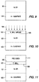
- the shallow well processing sequence of the invention begins with the deposition of a ubiquitous N-epitaxial layer 101 upon an underlying N+ silicon substrate 103, to a prescribed thickness and resistivity for a prescribed breakdown voltage device (e.g., having a thickness in a range on the order of from 3 ⁇ m to 24 ⁇ m and a resistivity on the order of from 0.2 ⁇ m to 5 ⁇ m).
- a prescribed breakdown voltage device e.g., having a thickness in a range on the order of from 3 ⁇ m to 24 ⁇ m and a resistivity on the order of from 0.2 ⁇ m to 5 ⁇ m.
- the top surface of the N- epitaxial layer 101 is subjected to a blanket implant of P-type impurities, to a prescribed depth (e.g., in a range on the order of from 0.05 ⁇ m to 0.3 ⁇ m) and dosage (e.g., in a range of from 8X10 12 atoms/cm 3 to 1.2X10 13 atoms/cm 3 ), thereby forming a very shallow P region 107 (e.g., to a depth on the order of 0.6 ⁇ m to 1.0 ⁇ m).
- This implant defines a PN junction 109 with N- epitaxial layer 101.
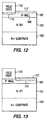
- a relatively thick field insulator (oxide) layer 111 (e.g., having a thickness on the order of from 8,000 to 12,000 angstroms) is then formed on the top surface 110 of the shallow P region 107 at the surface portion of the N- epitaxial layer 101, and then selectively etched, as shown in Figure 12, to form a field oxide mask 113, that overlies a first portion 115 of the shallow P well region 107, and exposes a second portion 117 of the shallow P well region 107, adjacent to the first surface portion 115.
- oxide oxide
- a gate insulator layer 121 is formed on the exposed portion 117 of the shallow P well region 107 to a thickness in a range on the order of from 200 to 1000 angstroms, and contiguous with field oxide layer 111.
- a polycrystalline silicon spacer layer 125 to be used to form a conductive gate layer, is non-selectively deposited to a thickness on the order of from 3000 Angstroms to 5000 Angstroms atop field oxide layer 111 and the gate insulator layer 121, as shown in Figure 14.
- a first portion 131 of the mask contains the compound thickness of the field oxide layer 113 and the polysilicon spacer layer 125 atop the field oxide layer 113.
- a second portion 133 of the mask contains a relatively thick portion 135 of the spacer layer 125 immediately adjacent to the side 112 of the field oxide layer 113 and the thickness of the gate insulator layer 121.
- the width or horizontal dimension of the second portion 135 of the mask defines the channel length between that portion of the well region beneath and aligned with the side edge 112 of the field oxide layer 113 and a PN junction formed between the well region and that portion of the well region that is converted to N type conductivity during a subsequent implant step, as will be described.
- the thicknesses of the first and second portions of the mask layer 130 are sufficient to block the penetration of dopant impurities during this implant step.
- a third portion 137 of the mask 130 contains only the thickness of the silicon spacer layer 125 and the gate insulator layer 121, so that it's reduced thickness allows the penetration of dopant impurities during the subsequent implant step.
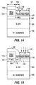
- the surface of the resulting structure is subjected to one or a plurality of high energy N+ impurity implants, shown at 141 in Figure 15, to overdose that portion 118 of the second portion 117 of the shallow P well region 107 underlying the third portion 137 of the mask 130, and thereby convert that portion of the P-well region 107 to N-type conductivity.
- This has the effect of extending the PN junction 109 up to the surface 114 of the well region beneath the gate insulator layer 121.
- This method uses polysilicon as an un-etched spacer for high energy N+ implants.
- the other obvious option is to non-selectively etch polysilicon and thereby create an etched polysilicon spacer.
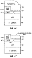
- a relatively thick (e.g., 0.3 microns) planarization layer of polysilicon 143 is non-selectively formed on the layer of polysilicon spacer layer 125.
- This step is followed by a planarization etch, shown in Figure 17, which serves to both planarize and reduce the thickness of the compound polysilicon material to the desired thickness of a polysilicon gate layer 145, having a level 147 below the thickness of the field insulator layer 113.
- the polysilicon gate layer 145 may have a thickness in a range on the order of from 5000 to 8000 angstroms.
- the field oxide layer 113 is stripped off with an oxide etch, such as a reactive ion dry etch, as shown in Figure 18, exposing surface portion 108 of the shallow P well region 107 adjacent to the gate oxide layer 121 and the polysilicon gate layer 145, which define a self-aligned mask for subsequent body and source implants.
- oxide etch such as a reactive ion dry etch
- an N+ source region 151 may be implanted into the shallow well adjacent to the side edge 153 of the polysilicon gate layer 145, using a separate photoresist mask, overlying the shallow P-well region 107, to define the size of the N+ source region 151.
- the N+ source region may 151 have an impurity concentration on the order of from 5X10 19 atoms/cm 3 to 2X10 20 atoms/cm 3 and a depth lying in a range on the order of from 0.1 ⁇ m to 0.3 ⁇ m.
- the channel region is defined as a silicon region in close proximity to gate oxide region located between source edge 155 and end of P-well region 160.
- a further P+ body implant is carried out, as shown in Figure 20, to form a surface P+ body region 161 in the P-well region 107.
- This implant may employ a dosage in a range of from 1X10 15 atoms/cm 3 to 1X10 16 atoms/cm 3 and depth in a range on the order of from 0.2 ⁇ m to 0.3 ⁇ m.
- the structure is then annealed for dopant activation and repair of damaged lattice sites.
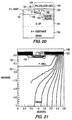
- Figure 21 diagrammatically illustrates the concentration of current flow during the on-state of a device manufactured in accordance with the processing sequence of Figures 9-20.
- the length of the channel within the shallow P-well channel is determined by the thickness of the polysilicon spacer layer, rather than by lateral and vertical diffusion of well dopant material as in the conventional device of Figures 1-8, what results is a shallow well insulated gate field effect device having decreased resistance and current pinching in the channel neck region, and thereby increased power handling capability and efficiency.
- a shallow well MOSFET including an epitaxial layer is subjected to a blanket implant of impurities, so as to form a very shallow well region that defines a PN junction with the epitaxial layer.
- a field oxide layer is selectively formed on a portion of the shallow well region, and a gate insulator layer is formed on the exposed portion of the shallow well region contiguous with the field insulator layer.
- a polycrystalline silicon spacer-gate layer is non-selectively deposited on the field insulator layer and the gate insulator layer, forming a multiple thickness implant mask.
- the structure is subjected to one or more high energy impurity implants, to overdose and convert a portion of the shallow well region to the conductivity of the epitaxial layer.
- a polysilicon planarization layer is then non-selectively formed on the spacer layer, followed by a planarization etch, to define the thickness of the gate layer.
- the field insulator layer is then stripped, and source and drain regions are formed.
Landscapes
- Insulated Gate Type Field-Effect Transistor (AREA)
- Metal-Oxide And Bipolar Metal-Oxide Semiconductor Integrated Circuits (AREA)
Applications Claiming Priority (2)
| Application Number | Priority Date | Filing Date | Title |
|---|---|---|---|
| US145513 | 1998-09-02 | ||
| US09/145,513 US6107127A (en) | 1998-09-02 | 1998-09-02 | Method of making shallow well MOSFET structure |
Publications (2)
| Publication Number | Publication Date |
|---|---|
| EP0984487A2 true EP0984487A2 (de) | 2000-03-08 |
| EP0984487A3 EP0984487A3 (de) | 2000-04-26 |
Family
ID=22513443
Family Applications (1)
| Application Number | Title | Priority Date | Filing Date |
|---|---|---|---|
| EP99115841A Withdrawn EP0984487A3 (de) | 1998-09-02 | 1999-08-11 | Methode zur Herstellung einer MOSFET-Struktur mit flacher Wanne |
Country Status (4)
| Country | Link |
|---|---|
| US (1) | US6107127A (de) |
| EP (1) | EP0984487A3 (de) |
| JP (1) | JP4791617B2 (de) |
| TW (1) | TW454252B (de) |
Cited By (1)
| Publication number | Priority date | Publication date | Assignee | Title |
|---|---|---|---|---|
| US6908823B2 (en) | 2002-12-30 | 2005-06-21 | Dongbuanam Semiconductor Inc. | Method of manufacturing a semiconductor device |
Families Citing this family (4)
| Publication number | Priority date | Publication date | Assignee | Title |
|---|---|---|---|---|
| US6358827B1 (en) * | 2001-01-19 | 2002-03-19 | Taiwan Semiconductor Manufacturing Company | Method of forming a squared-off, vertically oriented polysilicon spacer gate |
| JP4387291B2 (ja) * | 2004-12-06 | 2009-12-16 | パナソニック株式会社 | 横型半導体デバイスおよびその製造方法 |
| JP5014622B2 (ja) * | 2005-12-08 | 2012-08-29 | オンセミコンダクター・トレーディング・リミテッド | 絶縁ゲート型半導体装置の製造方法 |
| CN102468147B (zh) * | 2010-11-01 | 2017-11-28 | 中芯国际集成电路制造(上海)有限公司 | 一种半导体器件的栅极形成方法 |
Family Cites Families (8)
| Publication number | Priority date | Publication date | Assignee | Title |
|---|---|---|---|---|
| US4442589A (en) * | 1981-03-05 | 1984-04-17 | International Business Machines Corporation | Method for manufacturing field effect transistors |
| EP0250722A3 (de) * | 1986-07-04 | 1988-08-03 | Siemens Aktiengesellschaft | Verfahren zur Herstellung benachbarter, mit Dotierstoffionen unterschiedlichen Leitungstyps implantierter Wannen für hochintegrierte CMOS-Bauelemente |
| US4956700A (en) * | 1987-08-17 | 1990-09-11 | Siliconix Incorporated | Integrated circuit with high power, vertical output transistor capability |
| JP3200497B2 (ja) * | 1993-03-19 | 2001-08-20 | 三菱電機株式会社 | 電気的に情報の書込および消去が可能な半導体記憶装置およびその製造方法 |
| US5677215A (en) * | 1993-11-17 | 1997-10-14 | Lg Semicon Co., Ltd. | Method of fabricating a nonvolatile semiconductor memory device |
| US5538907A (en) * | 1994-05-11 | 1996-07-23 | Lsi Logic Corporation | Method for forming a CMOS integrated circuit with electrostatic discharge protection |
| US5478763A (en) * | 1995-01-19 | 1995-12-26 | United Microelectronics Corporation | High performance field effect transistor and method of manufacture thereof |
| DE19608003C2 (de) * | 1996-03-04 | 2001-11-29 | Daimler Chrysler Ag | Leistungs-Feldeffekt-Transistor und Verfahren zu seiner Herstellung |
-
1998
- 1998-09-02 US US09/145,513 patent/US6107127A/en not_active Expired - Lifetime
-
1999
- 1999-08-11 EP EP99115841A patent/EP0984487A3/de not_active Withdrawn
- 1999-08-24 TW TW088114463A patent/TW454252B/zh active
- 1999-09-02 JP JP24819999A patent/JP4791617B2/ja not_active Expired - Lifetime
Cited By (1)
| Publication number | Priority date | Publication date | Assignee | Title |
|---|---|---|---|---|
| US6908823B2 (en) | 2002-12-30 | 2005-06-21 | Dongbuanam Semiconductor Inc. | Method of manufacturing a semiconductor device |
Also Published As
| Publication number | Publication date |
|---|---|
| TW454252B (en) | 2001-09-11 |
| JP2000106437A (ja) | 2000-04-11 |
| US6107127A (en) | 2000-08-22 |
| JP4791617B2 (ja) | 2011-10-12 |
| EP0984487A3 (de) | 2000-04-26 |
Similar Documents
| Publication | Publication Date | Title |
|---|---|---|
| EP0580452B1 (de) | Feldeffekttransistor mit Graben mit niedrig dotiertem epitaktischen Gebiet an dessen Oberflächenbereich | |
| EP0948818B1 (de) | Hochdichte-graben-dmos-transistor mit grabenbodemimplantierung | |
| US5689128A (en) | High density trenched DMOS transistor | |
| EP0537684B1 (de) | Lateraler doppel-diffundierter MOS-Transistor und Verfahren zu seiner Herstellung | |
| US6624030B2 (en) | Method of fabricating power rectifier device having a laterally graded P-N junction for a channel region | |
| US6593619B1 (en) | High voltage power MOSFET having low on-resistance | |
| US6828195B2 (en) | Method of manufacturing a trench transistor having a heavy body region | |
| US5382536A (en) | Method of fabricating lateral DMOS structure | |
| US20020079521A1 (en) | Surface breakdown reduction by internal field rings and multiple poly field plates in power LDMOSFET | |
| WO1996030947A1 (en) | Punch-through field effect transistor | |
| JP2004522319A (ja) | ショットキー障壁を持つ半導体デバイスの製造 | |
| US20100090270A1 (en) | Trench mosfet with short channel formed by pn double epitaxial layers | |
| US6979861B2 (en) | Power device having reduced reverse bias leakage current | |
| KR20180097510A (ko) | 수직 전력 반도체 디바이스 내의 소스-게이트 영역 구조물 | |
| US6492679B1 (en) | Method for manufacturing a high voltage MOSFET device with reduced on-resistance | |
| KR20030085577A (ko) | 감소된 도통-저항을 갖는 이중 확산 전계 효과 트랜지스터 | |
| US6107127A (en) | Method of making shallow well MOSFET structure |
Legal Events
| Date | Code | Title | Description |
|---|---|---|---|
| PUAI | Public reference made under article 153(3) epc to a published international application that has entered the european phase |
Free format text: ORIGINAL CODE: 0009012 |
|
| AK | Designated contracting states |
Kind code of ref document: A2 Designated state(s): DE FR GB IT NL |
|
| AX | Request for extension of the european patent |
Free format text: AL;LT;LV;MK;RO;SI |
|
| PUAL | Search report despatched |
Free format text: ORIGINAL CODE: 0009013 |
|
| AK | Designated contracting states |
Kind code of ref document: A3 Designated state(s): AT BE CH CY DE DK ES FI FR GB GR IE IT LI LU MC NL PT SE |
|
| AX | Request for extension of the european patent |
Free format text: AL;LT;LV;MK;RO;SI |
|
| 17P | Request for examination filed |
Effective date: 20001006 |
|
| AKX | Designation fees paid |
Free format text: DE FR GB IT NL |
|
| 17Q | First examination report despatched |
Effective date: 20010521 |
|
| STAA | Information on the status of an ep patent application or granted ep patent |
Free format text: STATUS: THE APPLICATION IS DEEMED TO BE WITHDRAWN |
|
| 18D | Application deemed to be withdrawn |
Effective date: 20011002 |