EP0984535A2 - Halbleiterlaser mit Gitterstruktur - Google Patents
Halbleiterlaser mit Gitterstruktur Download PDFInfo
- Publication number
- EP0984535A2 EP0984535A2 EP99114805A EP99114805A EP0984535A2 EP 0984535 A2 EP0984535 A2 EP 0984535A2 EP 99114805 A EP99114805 A EP 99114805A EP 99114805 A EP99114805 A EP 99114805A EP 0984535 A2 EP0984535 A2 EP 0984535A2
- Authority
- EP
- European Patent Office
- Prior art keywords
- laser
- semiconductor laser
- layer
- lattice structure
- waveguide
- Prior art date
- Legal status (The legal status is an assumption and is not a legal conclusion. Google has not performed a legal analysis and makes no representation as to the accuracy of the status listed.)
- Granted
Links
- 239000004065 semiconductor Substances 0.000 title claims description 50
- 238000004519 manufacturing process Methods 0.000 claims abstract description 24
- 239000000758 substrate Substances 0.000 claims abstract description 14
- 238000000034 method Methods 0.000 claims description 30
- 230000008569 process Effects 0.000 claims description 18
- 229910052751 metal Inorganic materials 0.000 claims description 15
- 239000002184 metal Substances 0.000 claims description 15
- 239000000463 material Substances 0.000 claims description 12
- 230000005855 radiation Effects 0.000 claims description 10
- 238000000407 epitaxy Methods 0.000 claims description 5
- VYZAMTAEIAYCRO-UHFFFAOYSA-N Chromium Chemical compound [Cr] VYZAMTAEIAYCRO-UHFFFAOYSA-N 0.000 claims description 3
- 230000004888 barrier function Effects 0.000 claims description 3
- 238000001459 lithography Methods 0.000 claims description 3
- 238000001465 metallisation Methods 0.000 claims description 3
- 239000002131 composite material Substances 0.000 claims description 2
- 230000002093 peripheral effect Effects 0.000 claims description 2
- 239000000956 alloy Substances 0.000 claims 1
- 229910045601 alloy Inorganic materials 0.000 claims 1
- 235000012431 wafers Nutrition 0.000 description 16
- 238000001228 spectrum Methods 0.000 description 7
- 230000008878 coupling Effects 0.000 description 6
- 238000010168 coupling process Methods 0.000 description 6
- 238000005859 coupling reaction Methods 0.000 description 6
- 230000003321 amplification Effects 0.000 description 5
- 230000015572 biosynthetic process Effects 0.000 description 5
- 238000003199 nucleic acid amplification method Methods 0.000 description 5
- 230000000694 effects Effects 0.000 description 4
- 238000009413 insulation Methods 0.000 description 4
- 230000003287 optical effect Effects 0.000 description 4
- 230000007547 defect Effects 0.000 description 2
- 238000005530 etching Methods 0.000 description 2
- 238000002347 injection Methods 0.000 description 2
- 239000007924 injection Substances 0.000 description 2
- 238000005457 optimization Methods 0.000 description 2
- 208000012868 Overgrowth Diseases 0.000 description 1
- 238000010521 absorption reaction Methods 0.000 description 1
- 230000002411 adverse Effects 0.000 description 1
- 230000005540 biological transmission Effects 0.000 description 1
- 230000008859 change Effects 0.000 description 1
- 229910052804 chromium Inorganic materials 0.000 description 1
- 239000011651 chromium Substances 0.000 description 1
- 230000006735 deficit Effects 0.000 description 1
- 238000010586 diagram Methods 0.000 description 1
- 238000009826 distribution Methods 0.000 description 1
- 238000001312 dry etching Methods 0.000 description 1
- 238000010894 electron beam technology Methods 0.000 description 1
- 238000000609 electron-beam lithography Methods 0.000 description 1
- 239000000835 fiber Substances 0.000 description 1
- 238000002513 implantation Methods 0.000 description 1
- 238000007689 inspection Methods 0.000 description 1
- 238000003754 machining Methods 0.000 description 1
- 238000001000 micrograph Methods 0.000 description 1
- 230000035515 penetration Effects 0.000 description 1
- 230000002265 prevention Effects 0.000 description 1
- 238000002310 reflectometry Methods 0.000 description 1
- 230000002787 reinforcement Effects 0.000 description 1
- 239000000243 solution Substances 0.000 description 1
- 238000003892 spreading Methods 0.000 description 1
- 230000007480 spreading Effects 0.000 description 1
- 230000007704 transition Effects 0.000 description 1
Images


Classifications
-
- H—ELECTRICITY
- H01—ELECTRIC ELEMENTS
- H01S—DEVICES USING THE PROCESS OF LIGHT AMPLIFICATION BY STIMULATED EMISSION OF RADIATION [LASER] TO AMPLIFY OR GENERATE LIGHT; DEVICES USING STIMULATED EMISSION OF ELECTROMAGNETIC RADIATION IN WAVE RANGES OTHER THAN OPTICAL
- H01S5/00—Semiconductor lasers
- H01S5/10—Construction or shape of the optical resonator, e.g. extended or external cavity, coupled cavities, bent-guide, varying width, thickness or composition of the active region
- H01S5/12—Construction or shape of the optical resonator, e.g. extended or external cavity, coupled cavities, bent-guide, varying width, thickness or composition of the active region the resonator having a periodic structure, e.g. in distributed feedback [DFB] lasers
Definitions
- the present invention relates to a semiconductor laser with a Semiconductor substrate, a laser layer arranged on the semiconductor substrate, a waveguide bridge arranged at a distance from the laser layer and a strip-shaped one arranged parallel to the laser layer trained lattice structure.
- the present invention further relates to a method for producing such a semiconductor laser.
- DFB Distributed Feedback
- CMOS complementary metal-oxide-semiconductor
- CMOS complementary metal-oxide-semiconductor
- Wafer level based on a semiconductor substrate
- the lattice structure is formed in the laser layer about half the layer height of the epitaxial structure the epitaxial growth interrupted and in a lithography and removal process introduced the lattice structure. After that, the epitaxial growth continued. Due to the epitaxy interruption in the formation of the Laser layer and the subsequent overgrowth into the half layer introduced lattice structure, defects are induced in the laser layer, that adversely affect the properties of the laser layers and find themselves in a higher power consumption or in a express reduced life of the laser diodes.
- the properties one manufactured in the manner described above Semiconductor laser wafers cannot be specified exactly. Because the properties of the semiconductor laser wafer only after completion of the epitaxial growth and complete formation of the laser layer in the trial operation can be determined, the gain spectrum of the Semiconductor laser wafers only after formation of the lattice structure in the Laser layer can be determined so that no exact adjustment of the Lattice structure to the amplification spectrum of the laser layers possible and therefore the known DFB laser diodes are not exact according to defined specifications regarding the desired laser mode or the desired wavelength can be produced.
- the object of the present invention is now to provide a laser diode with a Propose structure that is simple and reproducible manufacture of laser diodes with a defined wavelength.
- a DFB laser diode propose with improved performance It is also the task of present invention, one for the production of an inventive DFB laser diode to propose a particularly suitable method.
- the inventive solution according to claim 1 enables a DFB laser diode with one after completion of the epitaxial growth of the laser layer for the completion of a semiconductor laser wafer and subsequently the structure of the waveguide web generated lattice structure. Because of this structure-related subsequent generation of the lattice structure it is possible to generate the individual gain spectrum before generating the lattice structure to determine the laser layer or the semiconductor laser wafer, in order to subsequently change the parameters of the Lattice structure to produce exactly the desired laser profile and so reproducible DFB laser diodes with precisely defined wavelength or To be able to produce laser fashion.
- the structure of the invention enables undisturbed, continuous formation of the laser layer in the epitaxy, so unnecessary defects that affect the performance characteristics of the laser layer or the DFB laser diode, do not occur at all.
- the lattice structure periodically modulates the Losses and the level of refraction of the laser spreading light.
- This enables the DFB laser diode according to the invention a complex coupling of the laser radiation with the lattice structure with a lateral modulation of the real and imaginary parts the refractive index.
- Laser diodes according to the invention therefore have a high reflectivity insensitivity to use without optical isolator, for example in applications for fiber optic transmission, makes possible.
- the grid structure can be adjusted as precisely as possible on a barrier or insulation layer arranged parallel to the laser layer be arranged.
- the metallic grid structure on a thin layer of insulation e.g. from natural or artificially produced oxide.
- the insulation layer should be chosen so that the refractive index is close to the refractive index of the semiconductor and the insulation is a small thickness has (typically a few nanometers). This layer is also used for Prevention of possible penetration of the semiconductor material Laser layers with the lattice material and thus also as a barrier layer.
- the advantageous described above Effects can be realized particularly comprehensively.
- the material selected to form the lattice structure can be the lattice structure also by removing material, not just one Material order.
- the structural areas of the Grid structure adjacent to the side flanks of the waveguide bridge are arranged and the width of the waveguide web is dimensioned so that Base points of the flanks in the peripheral area from the active zone of the Laser layer emitted radiation lie. This will make one possible little influence on the amplification power of the laser Lattice structure and in particular an effective coupling between the Laser radiation and the lattice structure ensured.
- flanks of the waveguide web are within the scope of the machining process achievable accuracy largely rectangular are arranged to the plane of extension of the lattice structure.
- the method according to the invention has the features of claim 6 on.
- the manufacture of a complete semiconductor laser structure in an epitaxy process with subsequent production of a Waveguide web by loading the semiconductor laser structure with a material removal process for training on both sides of the Carrier surfaces arranged on the waveguide web and subsequent Application of a lattice structure to the support surfaces.
- the lattice structure can also be removed by removing material can only be generated by a material order.
- the method according to the invention thus enables in a first method phase the production of functional laser diodes, resulting in a accurate inspection and determination of the electrical and optical Properties, for example a determination of the individual Gain spectrum of that used to manufacture the laser Semiconductor wafers, is possible. Only then are in a second Process phase the originally multi-mode laser diodes by generation of lattice structures defined in their parameters along the waveguide web to single-mode DFB laser diodes, each depending properties defined by the parameters of the lattice structures converted.
- a Insulating layer are formed.
- a particularly advantageous variant of the economically Manufacturing process becomes possible when producing a variety of DFB laser diodes with different properties first the manufacture of a semiconductor laser wafer by applying a Epitaxial structure takes place on a semiconductor substrate and then the generation of the waveguide webs assigned to the individual laser diodes takes place in the wafer network, that is, by generating one on the Surface of the semiconductor laser wafer arranged strip-shaped Waveguide structure with mutually parallel waveguide webs and intermediate support surfaces. Only after that the semiconductor laser wafer is divided into individual semiconductor laser chip units, then the exact definition of each Properties assigned to laser diodes via the application or Implantation of a lattice structure with the corresponding structural parameters on the surface of a selected number of laser diodes.
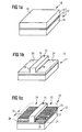
- FIG. 1a shows a semiconductor laser or a base laser diode 10 with a semiconductor substrate 11 and an epitaxial structure 12 grown thereon in a simplified representation and in a perspective view.
- Part of the epitaxial structure 12 is a laser layer 13, which is arranged on a buffer and contact layer 31 and is covered at the top by a cover layer 14.
- the base laser diode 10 shown in FIG. 1 a has a cuboid shape with a flat diode surface 16.
- the embodiment of a DFB laser diode 22 according to the invention shown in FIG. 1c is produced in two essential process phases, a waveguide diode 17 being shown in FIG. 1b as a transition form after carrying out a first process phase the diode surface 16 has been subjected to a material removal process, such as a dry etching process, in order to form the step-like surface configuration shown with a waveguide web 15 running in the longitudinal direction of the waveguide diode 17.
- the aforementioned material removal process creates surfaces formed on both sides by flanks 18, 19 of the waveguide web 15, which are referred to below as support surfaces 20 and 21, the support surfaces being covered by a thin insulating layer 26.
- the embodiment of a DFB laser diode 22 shown in FIG. 1c is produced by creating a metal grating structure 23 with two structure regions 24 and 25, which are each arranged in the carrier surfaces 20 and 21, by applying the Carrier surfaces 20 and 21 are produced using an electron beam lithography method and a subsequent metallization process, which is not described in more detail here.
- the result of this second process phase is the DFB laser diode 22 shown in FIG. 1c with the metal grating structure 23 arranged in the carrier surfaces 20 and 21 above the laser layer 13.
- the insulating layer 26 for example in the form of an etching stop layer, is provided in the epitaxial structure above the laser layer 13, which delimits the depth of a lithography structure in the epitaxial structure 12 produced using an etching process and thereby the relative position of the metal lattice structure 23 with respect to the Laser layer 13 defined.
- FIG. 2 shows a top view of the metal grating structure 23 shown schematically in FIG. 1c , the structural regions 24 and 25 constructed here from equidistantly spaced webs 27 extend up to the flanks 18 and 19 of the waveguide 15.
- the characteristic of the metal lattice structure 23 is determined on the one hand by the distance between the lattice webs 27 or the lattice constant d, the geometry of the lattice webs 27 and the metal used for the metal lattice structure 23.
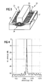
- the active zone 28 of the laser layer 13 is represented qualitatively by an intensity distribution shown in the exit cross section of the laser diode 22. It is clear that by directly connecting the individual lattice webs 27 to the flanks 18, 19 in an advantageous manner, in particular in the region of base points 29, 30 of the flanks 18, 19, a coupling between the metal lattice structure 23 and the laser radiation in its edge zone he follows.
- FIG. 4 makes the filter effect achieved by the metal grating structure 23 clear, since, as can be seen from FIG. 4 , secondary modes of the laser radiation emitted from the active zone 28 are effectively suppressed and essentially only the emission of a laser mode with a precisely defined wavelength is permitted.
- Fig. 5 shows the effects of changes in the grating constant d ( Fig. 1c ) on the wavelength.
- Fig. 5 makes it clear that by changing the grating constant d, a highly precise fine-tuning of the wavelength is possible, so that starting from a predetermined individual amplification spectrum of a basic laser diode 10 shown by way of example in Fig. 1a , by selective selection of the parameters of the grating structure, for example here the grating constant , a highly precise setting of the wavelength for the intended application of the laser diode in question is adjustable.
- the complex coupling between the laser radiation and the grating structure that is to say the absolute size and the relative ratio of the real and imaginary part of the refractive index - and thus the part of refractive index coupling and absorption coupling - can be broad Limits can be set.
- the so-called "duty cycle" of the lattice structure that is to say the ratio of the lattice web width to the lattice constant, also represents an optimization variable.
Landscapes
- Physics & Mathematics (AREA)
- Condensed Matter Physics & Semiconductors (AREA)
- General Physics & Mathematics (AREA)
- Electromagnetism (AREA)
- Optics & Photonics (AREA)
- Semiconductor Lasers (AREA)
- Lasers (AREA)
Abstract
Description
- Fig. 1a bis 1c
- verschiedene Stadien bei der Herstellung einer DFB-Laserdiode mit lateraler Gitterstruktur;
- Fig. 2
- eine Rasterelektronenaufnahme unter Darstellung einer Draufsicht auf die beidseitig eines Wellenleiters angeordnete Gitterstruktur;
- Fig. 3
- eine vereinfachte perspektivische Darstellung einer Laserdiode mit Darstellung der aktiven Zone einer Laserschicht;
- Fig. 4
- eine Diagrammdarstellung eines möglichen Verstärkungsspektrums der in Fig. 3 dargestellten Laserdiode;
- Fig. 5
- eine graphische Darstellung der Abhängigkeit zwischen dem Verstärkungsspektrum bzw. der Wellenlänge der von der Laserdiode emittierten Strahlung und der Gitterkonstante der Gitterstruktur.
Claims (9)
- Halbleiterlaser mit einem Halbleitersubstrat, einer auf dem Halbleitersubstrat angeordneten Laserschicht, einem mit Abstand zur Laserschicht angeordneten Wellenleitersteg und einer parallel zur Laserschicht angeordneten, streifenförmig ausgebildeten Gitterstruktur,
dadurch gekennzeichnet,
daß die Gitterstruktur (23) zwei Strukturbereiche (24, 25) aufweist, die beidseitig des Wellenleiterstegs (15) angeordnet und mit Abstand zur Laserschicht (13) oberhalb der Laserschicht (13) ausgebildet sind. - Halbleiterlaser nach Anspruch 1,
dadurch gekennzeichnet,
daß die Gitterstruktur (23) auf einer die Relativlage der Gitterstruktur zur Laserschicht (13) definierenden Barrieren- oder Isolierschicht (26) angeordnet ist. - Halbleiterlaser nach Anspruch 1 oder 2,
dadurch gekennzeichnet,
daß die Gitterstruktur (23) aus Metall, insbesondere Chrom oder einer Chromlegierung, hergestellt ist. - Halbleiterlaser nach einem oder mehreren der vorangehenden Ansprüche,
dadurch gekennzeichnet,
daß die Strukturbereiche (24, 25) der Gitterstruktur (23, 31) angrenzend an seitliche Flanken (18, 19) des Wellenleiterstegs (15) angeordnet sind, und die Breite des Wellenleiterstegs so bemessen ist, daß Fußpunkte (29, 30) der Flanken im Peripheriebereich der aus einer aktiven Zone (28) der Laserschicht (13) emittierten Strahlung liegen. - Halbleiterlaser nach Anspruch 4,
dadurch gekennzeichnet,
daß die Flanken (18, 19) des Wellenleiterstegs (15) im wesentlichen rechtwinkelig zur Erstreckungsebene der Gitterstruktur (23, 31) angeordnet sind. - Verfahren zur Herstellung eines Halbleiterlasers basierend auf einem Halbleitersubstrat mit einer auf dem Halbleitersubstrat angeordneten Laserschicht und einer streifenförmig ausgebildeten Gitterstruktur,
gekennzeichnet durch die Verfahrensschritte:Herstellung einer vollständigen Halbleiterlaserstruktur in einem Epitaxieverfahren,Herstellung eines Wellenleiterstegs (15) durch Beaufschlagung der Halbleiterlaserstruktur mit einem Materialabtragsverfahren zur Ausbildung von beidseitig des Wellenleiterstegs (15) angeordneten Trägerflächen (20, 21),Aufbringung der Gitterstruktur (23) auf die Trägerflächen. - Verfahren nach Anspruch 6,
dadurch gekennzeichnet,
daß vor Aufbringung der Gitterstruktur (23) auf die Trägerflächen (20, 21) auf diesen eine Isolierschicht (26) ausgebildet wird. - Verfahren nach Anspruch 6 oder 7,
dadurch gekennzeichnet,
daß zur Aufbringung einer Gitterstruktur (23) aus Metall, ein Lithographieverfahren mit nachfolgender Metallisierung der lithographischen Struktur eingesetzt wird. - Verfahren nach einem oder mehreren der Ansprüche 6 bis 7,
dadurch gekennzeichnet,
daß eine Vielzahl von Halbleiterlasern in einem Waferverbund hergestellt wird mit den Verfahrensschritten:Herstellung eines Halbleiterlaserwafers durch Aufbringung einer Epitaxiestruktur (12) auf ein Halbleitersubstrat (11),Erzeugung einer auf der Oberfläche des Halbleiterlaserwafers angeordneten stegförmigen Wellenleiterstruktur mit zueinander parallelen Wellenleiterstegen (15),Zerteilung des Halbleiterlaserwafers in einzelne Halbleiterlaserchipeinheiten,Erzeugung einer oder mehrerer Gitterstrukturen (23, 31) auf den Halbleiterlaserchipeinheiten.
Applications Claiming Priority (4)
| Application Number | Priority Date | Filing Date | Title |
|---|---|---|---|
| DE29815522U DE29815522U1 (de) | 1998-08-31 | 1998-08-31 | Halbleiterlaser mit Gitterstruktur |
| DE29815522U | 1998-08-31 | ||
| US296059 | 1999-04-21 | ||
| US09/296,059 US6671306B1 (en) | 1998-08-31 | 1999-04-21 | Semiconductor laser with a lattice structure |
Publications (3)
| Publication Number | Publication Date |
|---|---|
| EP0984535A2 true EP0984535A2 (de) | 2000-03-08 |
| EP0984535A3 EP0984535A3 (de) | 2001-06-27 |
| EP0984535B1 EP0984535B1 (de) | 2005-08-17 |
Family
ID=26061788
Family Applications (1)
| Application Number | Title | Priority Date | Filing Date |
|---|---|---|---|
| EP99114805A Expired - Lifetime EP0984535B1 (de) | 1998-08-31 | 1999-07-28 | Halbleiterlaser mit Gitterstruktur |
Country Status (5)
| Country | Link |
|---|---|
| US (1) | US6846689B2 (de) |
| EP (1) | EP0984535B1 (de) |
| AT (1) | ATE302483T1 (de) |
| DK (1) | DK0984535T3 (de) |
| ES (1) | ES2247750T3 (de) |
Cited By (3)
| Publication number | Priority date | Publication date | Assignee | Title |
|---|---|---|---|---|
| JP2003110193A (ja) * | 2001-08-06 | 2003-04-11 | Nanoplus Gmbh Nanosystems & Technologies | 弱く結合されたグレーティングを有する半導体レーザ |
| US8855156B2 (en) | 2009-05-05 | 2014-10-07 | Nanoplus Gmbh Nanosystems And Technologies | DFB laser diode having a lateral coupling for large output power |
| US12308610B2 (en) | 2020-03-13 | 2025-05-20 | Advanced Photonics Applications Gmbh | Single mode semiconductor laser with phase control |
Families Citing this family (6)
| Publication number | Priority date | Publication date | Assignee | Title |
|---|---|---|---|---|
| EP1343232B1 (de) * | 2002-03-08 | 2007-05-02 | nanoplus GmbH Nanosystems and Technologies | Ein Halbleiterlaserarray mit seitlicher Gratingstruktur |
| US7301977B2 (en) * | 2004-06-10 | 2007-11-27 | Nanoplus Gmbh | Tuneable unipolar lasers |
| US10326037B1 (en) | 2018-08-27 | 2019-06-18 | Quantum Photonics Corporation | Photonic energy storage device |
| US11714009B2 (en) * | 2018-09-26 | 2023-08-01 | Battelle Energy Alliance, Llc | Ultrasonic sensors and methods of using the ultrasonic sensors |
| EP3832817B1 (de) | 2019-12-03 | 2025-07-23 | Advanced Photonics Applications GmbH | Halbleiterlaser sowie verfahren zur herstellung eines halbleiterlasers |
| CN117913650B (zh) * | 2023-12-14 | 2025-09-26 | 长春理工大学 | 一种双波长输出的半导体激光器及其制备方法 |
-
1999
- 1999-07-28 AT AT99114805T patent/ATE302483T1/de active
- 1999-07-28 EP EP99114805A patent/EP0984535B1/de not_active Expired - Lifetime
- 1999-07-28 DK DK99114805T patent/DK0984535T3/da active
- 1999-07-28 ES ES99114805T patent/ES2247750T3/es not_active Expired - Lifetime
-
2003
- 2003-10-02 US US10/677,903 patent/US6846689B2/en not_active Expired - Lifetime
Non-Patent Citations (5)
| Title |
|---|
| CHEN N ET AL: "1.3- mu m wavelength InP laterally coupled distributed feedback ridge laser" CONFERENCE ON OPTICAL FIBER COMMUNICATIONS. TECHNICAL DIGEST. POSTCONFERENCE EDITION. 1997 OSA TECHNICAL DIGEST SERIES. VOL.6 (IEEE CAT. NO.97CH36049), PROCEEDINGS OF OPTICAL FIBER COMMUNICATION CONFERENCE (ISBN 1 55752 481 5), DALLAS, TX, USA, 16-21, Seiten 237-238, XP002164961 1997, Washington, DC, USA, Opt. Soc. America, USA ISBN: 1-55752-480-7 * |
| KAMP M ET AL: "High performance laterally gain coupled InGaAs/AlGaAs DFB lasers" CONFERENCE PROCEEDINGS. 1998 INTERNATIONAL CONFERENCE ON INDIUM PHOSPHIDE AND RELATED MATERIALS (CAT. NO.98CH36129), CONFERENCE PROCEEDINGS. 1998 INTERNATIONAL CONFERENCE ON INDIUM PHOSPHIDE AND RELATED MATERIALS, TSUKUBA, JAPAN, 11-15 MAY 1998, Seiten 831-834, XP000998200 1998, New York, NY, USA, IEEE, USA ISBN: 0-7803-4220-8 * |
| KAMP M ET AL: "LOW-THRESHOLD HIGH-QUANTUM-EFFICIENCY LATERALLY GAIN-COUPLED INGAAS/AIGAAS DISTRIBUTED FEEDBACK LASERS" APPLIED PHYSICS LETTERS,US,AMERICAN INSTITUTE OF PHYSICS. NEW YORK, Bd. 74, Nr. 4, 25. Januar 1999 (1999-01-25), Seiten 483-485, XP000805752 ISSN: 0003-6951 * |
| LEGGE M ET AL: "Low threshold II-VI laser diodes with transversal and longitudinal single-mode emission" JOURNAL OF CRYSTAL GROWTH,NORTH-HOLLAND PUBLISHING CO. AMSTERDAM,NL, Bd. 214-215, Juni 2000 (2000-06), Seiten 1045-1048, XP004201167 ISSN: 0022-0248 * |
| MARTIN R D ET AL: "CW PERFORMANCE OF AN INGAAS-GAAS-ALGAAS LATERALLY-COUPLED DISTRIBUTED FEEDBACK (LC-DFB) RIDGE LASER DIODE" IEEE PHOTONICS TECHNOLOGY LETTERS,US,IEEE INC. NEW YORK, Bd. 7, Nr. 3, 1. M{rz 1995 (1995-03-01), Seiten 244-246, XP000510265 ISSN: 1041-1135 * |
Cited By (3)
| Publication number | Priority date | Publication date | Assignee | Title |
|---|---|---|---|---|
| JP2003110193A (ja) * | 2001-08-06 | 2003-04-11 | Nanoplus Gmbh Nanosystems & Technologies | 弱く結合されたグレーティングを有する半導体レーザ |
| US8855156B2 (en) | 2009-05-05 | 2014-10-07 | Nanoplus Gmbh Nanosystems And Technologies | DFB laser diode having a lateral coupling for large output power |
| US12308610B2 (en) | 2020-03-13 | 2025-05-20 | Advanced Photonics Applications Gmbh | Single mode semiconductor laser with phase control |
Also Published As
| Publication number | Publication date |
|---|---|
| ES2247750T3 (es) | 2006-03-01 |
| ATE302483T1 (de) | 2005-09-15 |
| DK0984535T3 (da) | 2005-12-12 |
| US6846689B2 (en) | 2005-01-25 |
| US20040072379A1 (en) | 2004-04-15 |
| EP0984535B1 (de) | 2005-08-17 |
| EP0984535A3 (de) | 2001-06-27 |
Similar Documents
| Publication | Publication Date | Title |
|---|---|---|
| DE3936694C2 (de) | Halbleiterbauteil, insbesondere DFB-Halbleiterlaser | |
| DE4025144C2 (de) | ||
| DE60224273T2 (de) | Mehrstrahlhalbleiterlasereinrichtung | |
| DE102008025922B4 (de) | Kantenemittierender Halbleiterlaser mit Phasenstruktur | |
| DE3445725A1 (de) | Halbleiter-laservorrichtung | |
| DE69521556T2 (de) | Herstellungsverfahren für eine optische Halbleitervorrichtung | |
| DE112009003752B4 (de) | Verfahren zur Herstellung einer Fotovoltaikvorrichtung | |
| EP1283571A1 (de) | Laser mit schwach gekoppeltem Gitterbereich | |
| DE19619533A1 (de) | Monolithisch integriertes optisches Halbleiterbauelement | |
| DE69407507T2 (de) | Halbleitende optische Vorrichtung mit Mesa-Struktur, die seitlich von einer isolierenden Maske umgeben ist | |
| DE19637163A1 (de) | Halbleiterlaser und Verfahren zur Herstellung des Halbleiterlasers | |
| EP0984535B1 (de) | Halbleiterlaser mit Gitterstruktur | |
| DE29815522U1 (de) | Halbleiterlaser mit Gitterstruktur | |
| EP2942848B1 (de) | Halbleiterlaser sowie verfahren zur herstellung eines halbleiterlasers umfassend ein rückkopplungselement | |
| DE10302134A1 (de) | Halbleiterlaser | |
| DE4034187A1 (de) | Optisches halbleiterelement | |
| DE4432410A1 (de) | Optoelektronisches Multi-Wellenlängen Bauelement | |
| DE102008040374A1 (de) | Lasereinrichtung | |
| DE2652870A1 (de) | Lasermatrixanordnung in planartechnik | |
| DE60203701T2 (de) | Halbleiterlaser mit einer vielzahl von optisch aktiven gebieten | |
| DE19613235A1 (de) | Selektive Maske, Herstellungsverfahren für ein optisches Halbleiterbauelement und optisches Halbleiterbauelement | |
| DE10245544B4 (de) | Distributed-Feedback-Laservorrichtung | |
| DE60204702T2 (de) | Verbesserungen für optische vorrichtungen | |
| DE60116827T2 (de) | InGaAsP-Halbleiterlaser | |
| DE602004008096T2 (de) | Steuerung der ausgangsstrahldivergenz in einem halbleiterwellenleiterbauelement |
Legal Events
| Date | Code | Title | Description |
|---|---|---|---|
| PUAI | Public reference made under article 153(3) epc to a published international application that has entered the european phase |
Free format text: ORIGINAL CODE: 0009012 |
|
| AK | Designated contracting states |
Kind code of ref document: A2 Designated state(s): AT BE CH CY DE DK ES FI FR GB GR IE IT LI LU MC NL PT SE |
|
| AX | Request for extension of the european patent |
Free format text: AL;LT;LV;MK;RO;SI |
|
| PUAL | Search report despatched |
Free format text: ORIGINAL CODE: 0009013 |
|
| AK | Designated contracting states |
Kind code of ref document: A3 Designated state(s): AT BE CH CY DE DK ES FI FR GB GR IE IT LI LU MC NL PT SE |
|
| AX | Request for extension of the european patent |
Free format text: AL;LT;LV;MK;RO;SI |
|
| 17P | Request for examination filed |
Effective date: 20011220 |
|
| AKX | Designation fees paid |
Free format text: AT BE CH CY DE DK ES FI FR GB GR IE IT LI LU MC NL PT SE |
|
| 17Q | First examination report despatched |
Effective date: 20040126 |
|
| GRAP | Despatch of communication of intention to grant a patent |
Free format text: ORIGINAL CODE: EPIDOSNIGR1 |
|
| GRAS | Grant fee paid |
Free format text: ORIGINAL CODE: EPIDOSNIGR3 |
|
| GRAA | (expected) grant |
Free format text: ORIGINAL CODE: 0009210 |
|
| AK | Designated contracting states |
Kind code of ref document: B1 Designated state(s): AT BE CH CY DE DK ES FI FR GB GR IE IT LI LU MC NL PT SE |
|
| REG | Reference to a national code |
Ref country code: GB Ref legal event code: FG4D Free format text: NOT ENGLISH |
|
| REG | Reference to a national code |
Ref country code: CH Ref legal event code: EP |
|
| REG | Reference to a national code |
Ref country code: IE Ref legal event code: FG4D Free format text: LANGUAGE OF EP DOCUMENT: GERMAN |
|
| REF | Corresponds to: |
Ref document number: 59912422 Country of ref document: DE Date of ref document: 20050922 Kind code of ref document: P |
|
| REG | Reference to a national code |
Ref country code: SE Ref legal event code: TRGR |
|
| REG | Reference to a national code |
Ref country code: DK Ref legal event code: T3 |
|
| REG | Reference to a national code |
Ref country code: CH Ref legal event code: NV Representative=s name: HEPP, WENGER & RYFFEL AG |
|
| GBT | Gb: translation of ep patent filed (gb section 77(6)(a)/1977) |
Effective date: 20051130 |
|
| REG | Reference to a national code |
Ref country code: GR Ref legal event code: EP Ref document number: 20050403766 Country of ref document: GR |
|
| REG | Reference to a national code |
Ref country code: ES Ref legal event code: FG2A Ref document number: 2247750 Country of ref document: ES Kind code of ref document: T3 |
|
| ET | Fr: translation filed | ||
| PLBE | No opposition filed within time limit |
Free format text: ORIGINAL CODE: 0009261 |
|
| STAA | Information on the status of an ep patent application or granted ep patent |
Free format text: STATUS: NO OPPOSITION FILED WITHIN TIME LIMIT |
|
| 26N | No opposition filed |
Effective date: 20060518 |
|
| PG25 | Lapsed in a contracting state [announced via postgrant information from national office to epo] |
Ref country code: MC Free format text: LAPSE BECAUSE OF NON-PAYMENT OF DUE FEES Effective date: 20060731 |
|
| PG25 | Lapsed in a contracting state [announced via postgrant information from national office to epo] |
Ref country code: LU Free format text: LAPSE BECAUSE OF NON-PAYMENT OF DUE FEES Effective date: 20060728 |
|
| PG25 | Lapsed in a contracting state [announced via postgrant information from national office to epo] |
Ref country code: CY Free format text: LAPSE BECAUSE OF FAILURE TO SUBMIT A TRANSLATION OF THE DESCRIPTION OR TO PAY THE FEE WITHIN THE PRESCRIBED TIME-LIMIT Effective date: 20050817 |
|
| REG | Reference to a national code |
Ref country code: FR Ref legal event code: PLFP Year of fee payment: 18 |
|
| REG | Reference to a national code |
Ref country code: FR Ref legal event code: PLFP Year of fee payment: 19 |
|
| REG | Reference to a national code |
Ref country code: FR Ref legal event code: PLFP Year of fee payment: 20 |
|
| PGFP | Annual fee paid to national office [announced via postgrant information from national office to epo] |
Ref country code: IT Payment date: 20180720 Year of fee payment: 20 Ref country code: FR Payment date: 20180723 Year of fee payment: 20 Ref country code: DE Payment date: 20180725 Year of fee payment: 20 Ref country code: NL Payment date: 20180723 Year of fee payment: 20 Ref country code: IE Payment date: 20180720 Year of fee payment: 20 Ref country code: ES Payment date: 20180829 Year of fee payment: 20 |
|
| PGFP | Annual fee paid to national office [announced via postgrant information from national office to epo] |
Ref country code: DK Payment date: 20180725 Year of fee payment: 20 Ref country code: AT Payment date: 20180719 Year of fee payment: 20 Ref country code: GB Payment date: 20180725 Year of fee payment: 20 Ref country code: SE Payment date: 20180725 Year of fee payment: 20 Ref country code: CH Payment date: 20180725 Year of fee payment: 20 Ref country code: GR Payment date: 20180724 Year of fee payment: 20 Ref country code: FI Payment date: 20180719 Year of fee payment: 20 Ref country code: BE Payment date: 20180723 Year of fee payment: 20 |
|
| PGFP | Annual fee paid to national office [announced via postgrant information from national office to epo] |
Ref country code: PT Payment date: 20180718 Year of fee payment: 20 |
|
| REG | Reference to a national code |
Ref country code: DE Ref legal event code: R071 Ref document number: 59912422 Country of ref document: DE |
|
| REG | Reference to a national code |
Ref country code: DK Ref legal event code: EUP Effective date: 20190728 |
|
| REG | Reference to a national code |
Ref country code: CH Ref legal event code: PL Ref country code: NL Ref legal event code: MK Effective date: 20190727 |
|
| REG | Reference to a national code |
Ref country code: GB Ref legal event code: PE20 Expiry date: 20190727 Ref country code: IE Ref legal event code: MK9A |
|
| REG | Reference to a national code |
Ref country code: BE Ref legal event code: MK Effective date: 20190728 |
|
| REG | Reference to a national code |
Ref country code: AT Ref legal event code: MK07 Ref document number: 302483 Country of ref document: AT Kind code of ref document: T Effective date: 20190728 |
|
| PG25 | Lapsed in a contracting state [announced via postgrant information from national office to epo] |
Ref country code: PT Free format text: LAPSE BECAUSE OF EXPIRATION OF PROTECTION Effective date: 20190806 Ref country code: IE Free format text: LAPSE BECAUSE OF EXPIRATION OF PROTECTION Effective date: 20190728 |
|
| PG25 | Lapsed in a contracting state [announced via postgrant information from national office to epo] |
Ref country code: GB Free format text: LAPSE BECAUSE OF EXPIRATION OF PROTECTION Effective date: 20190727 |
|
| REG | Reference to a national code |
Ref country code: ES Ref legal event code: FD2A Effective date: 20220126 |
|
| PG25 | Lapsed in a contracting state [announced via postgrant information from national office to epo] |
Ref country code: ES Free format text: LAPSE BECAUSE OF EXPIRATION OF PROTECTION Effective date: 20190729 |