EP0984609A2 - Verfahren und Vorrichtung zur vielkanal-Echounterdruckung - Google Patents
Verfahren und Vorrichtung zur vielkanal-Echounterdruckung Download PDFInfo
- Publication number
- EP0984609A2 EP0984609A2 EP99250302A EP99250302A EP0984609A2 EP 0984609 A2 EP0984609 A2 EP 0984609A2 EP 99250302 A EP99250302 A EP 99250302A EP 99250302 A EP99250302 A EP 99250302A EP 0984609 A2 EP0984609 A2 EP 0984609A2
- Authority
- EP
- European Patent Office
- Prior art keywords
- signals
- signal
- time
- received signal
- linear
- Prior art date
- Legal status (The legal status is an assumption and is not a legal conclusion. Google has not performed a legal analysis and makes no representation as to the accuracy of the status listed.)
- Granted
Links
Images












Classifications
-
- H—ELECTRICITY
- H03—ELECTRONIC CIRCUITRY
- H03H—IMPEDANCE NETWORKS, e.g. RESONANT CIRCUITS; RESONATORS
- H03H21/00—Adaptive networks
- H03H21/0012—Digital adaptive filters
Definitions
- the present invention relates to a method and an apparatus for canceling echoes in a system using plural received signals and a single or plural transmission signals.
- multi-channel echo canceling methods or apparatuses that remove echoes caused by received signals propagating through spatial acoustic paths in the system of transmitting plural received signals or a single or plural transmission signals.
- Two types of multi-channel echo canceling apparatuses including a cascade connection type and a linear coupled type have been proposed in the Technical Report of the Institute of Electronics, Information and Communication Engineers (IEICE) of Japan, Vol. 84, No. 330, pp. 7-14, CS-84-178 (hereinafter referred to as reference 1).
- the cascade connection type is inferior to the linear coupled type in echo suppression capability caused by constitutional constraint.
- a linear coupled multi-channel echo canceling apparatus echo canceller
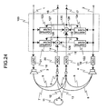
- Fig. 24 shows a linear coupled multi-channel echo canceller.
- the first loudspeaker 3 reproduces the first received signal 1.
- the second loudspeaker 4 reproduces the second received signal 2.
- the first echo 5 which is generated as the signal propagating via spatial acoustic paths from the first loudspeaker 3 to the first microphone 9 and the second echo 6 which is produced as the signal propagating through spatial acoustic paths from the second loudspeaker 4 to the first microphone 9 are added to the first transmission signal 12 or the voice of the talker 11 received with the first microphone 9, so that a first mixed signal 14 is created.
- the third echo 7 which is generated as the signal propagating the spatial acoustic paths from the first loudspeaker 3 to the second microphone 10 and the fourth echo 8 which is produced as the signal propagating through spatial acoustic paths from the second loudspeaker 4 to the second microphone 10 are added to the second transmission signal 13 or the voice of the talker 11 received with the second microphone 10, so that a second mixed signal 15 is created.
- the first adaptive filter 121 receives the first received signal 1 and then creates an echo replica 125 corresponding to the first echo 5.
- the second adaptive filter 122 receives the second received signal 2 and then creates an echo replica 126 corresponding to the second echo 6.
- the first subtracter 129 subtracts the echo replicas 125 and 126 corresponding to the first echo 5 and the second echo 6, respectively, from the first mixed signal 14.
- the first and second adaptive filters 121 and 122 are controlled to minimize the output of the first subtracter 129.
- the output of the first subtracter 129 becomes the first output signal 16 of the echo canceller 100.
- the third adaptive filter 123 receives the first received signal 1 and then creates an echo replica 127 corresponding to the third echo 7.
- the fourth adaptive filter 124 receives the second received signal 2 and then creates an echo replica 128 corresponding to the fourth echo 8.
- the second subtracter 130 subtracts the replicas 127 and 128 corresponding to the third echo 7 and the fourth echo 8 from the second mixed signal 15, respectively.
- the third and fourth adaptive filters 123 and 124 are controlled to minimize the output of the second subtracter 130.
- the output of the second subtracter 130 becomes the second output signal 17 of the echo canceller 100.
- x 1 (n) is a first received signal 1 at the time n
- x 2 (n) is a second received signal 2 at the time n
- d(n) is an echo introduced into the mixed signal 14.
- the echo d(n) mixed in the mixed signal 14 is the sum of the echo 5 and the echo 6 and is expressed by: where h 1,j is an impulse response sample value of a spatial acoustic path ranging from the loudspeaker 3 to the microphone 9, h 2,i is an impulse response sample value of a spatial acoustic path ranging from the loudspeaker 4 to the microphone 9, and i is an integer value between 0 and N-1.
- the echo replica d(n) hat created by each of the adaptive filters 121 and 122 is expressed by: where w 1,i (n) is the i-th filter coefficient of the adaptive filter 121 and w 2,i (n) is the i-th filter coefficient of the adaptive filter 122.
- the multi-channel echo canceling method of the reference 2 can avoid indefinite solutions because one adaptive filter removes the echo generated in one channel. As a result, the adaptive filter coefficients are converged to optimum values which are uniquely determined.
- the reference 2 discloses evaluation results proving the fact that the echo suppression is degraded when the parameters determined by the environment in use such as the locations of microphones receiving the taker s voice are not within a certain range.
- a multi-channel echo canceller based on linear combination has to be used, by considering the use in a wide variety of environments.
- reference 5 303-306
- the method disclosed in reference 4 provides a slow convergence rate, compared with the multi-channel echo canceller based on linear combination.
- reference 6 discloses that the method in the reference 5 provides a slower convergence rate, compared with the method in reference 4.
- the conventional multi-channel echo canceling method and apparatus has the disadvantage in that the solutions to adaptive filter coefficients are indefinite and are not guaranteed to be equal to the solutions uniquely determined by the impulse responses in the echo paths. Moreover, in the method proposed in reference 3, a shift of an acoustic (or sound) image may often be perceived when the received signal or the delayed received signal is selected. Moreover, in the methods proposed in the references 4 and 5, the convergence is slow, compared with the conventional multi-channel echo canceling method or apparatus.
- the objective of the invention is to provide a multi-channel echo canceling method and/or apparatus with an excellent sound quality and a short convergence time, wherein the coefficient values of the adaptive filters are converged to correct values which are uniquely determined by the impulse responses of the echo paths.
- received signals are non-linearly processed while one obtained by delaying a received signal is used as a new received signal.
- the multi-channel echo canceling apparatus has magnitude processing circuits for non-linearly processing received signals and a delay processing circuit for delaying the received signal 2 and then supplying the delayed signal to adaptive filters and to a digital-to-analog converter (DAC).
- magnitude processing circuits for non-linearly processing received signals
- delay processing circuit for delaying the received signal 2 and then supplying the delayed signal to adaptive filters and to a digital-to-analog converter (DAC).
- DAC digital-to-analog converter
- the multi-channel echo canceling apparatus non-linearly processes the received signals.
- the multi-channel echo canceling apparatus also uses a delayed received signal as a new received signal and applies magnitude correction to the other input signals.
- the multi-channel echo canceling apparatus has a magnitude processing circuit for non-linearly processing the received signal, a delay processing circuit for delaying a non-linearly processed signal and then supplying the delayed signal to the adaptive filters 122 and 124 and the digital-to-analog converter, a magnitude processing circuit for non-linearly processing the received signal, and a magnitude compensating circuit for correcting the magnitude of the non-linearly processed signal and then supplying the corrected signal to the adaptive filters and the digital-to-analog converter.
- one received signal is filtered to create a supplement signal.
- the adaptive filter is operated using a new signal obtained by time-multiplexing an original received signal and the created supplement signal.
- a plurality of adaptive filters estimate echoes caused by propagating from one signal source in plural paths. For that reason, an increase in the number of conditions for solving adaptive filter coefficients makes solutions definite eliminating the existing problem of indefinite coefficients. Hence, the adaptive filter coefficients are converged to optimum values which are uniquely determined.
- the multiplex parameters of the original received signal and the supplement signal are controlled based on the nature of the received signal while movement of the sound image caused by introducing the supplement signal is canceled in the magnitude correction process to the input signal.
- Embodiments of the present invention will be described in detail below with reference to Figs. 1 to 23. It is now assumed to use a two-channel acoustic echo canceller that has a first received signal, a second received signal, a first mixed signal and a second mixed signal. This acoustic echo canceller can remove acoustic echoes caused by received signals propagating from a loudspeaker to a microphone via a spatial acoustic path.
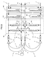
- Fig. 1 shows a multi-channel echo canceller with two received signals and two transmission signals, according to an embodiment of the present invention.
- This multi-channel echo canceller differs from the multi-channel echo canceller based on linear combination of Fig. 24 in that the non-linear processing circuit 600 and the pre-processing circuit 500 process the received signal 2 supplied to the adaptive filters 122 and 124.
- the first mixed signal 14 and the second mixed signal 15 are created in a similar manner to that of the multi-channel echo canceller based on linear combination shown in Fig. 24.
- the magnitude processing circuit 605 non-linearly processes the received signal 2 while the magnitude processing circuit 606 non-linearly processes the received signal 1.
- the first and the second received signals 1 and 2 which are non-linearly processed, are transferred to the processing circuit 500. If there is a slight difference between the received signals 1 and 2, the non-linear process enlarges it, thus, reducing the correlation between the received signals in these channels. This means that the adaptive filter coefficients are properly identified. However, as described earlier, the non-linear processing alone results in a slow convergence rate. For that reason, it is intended to further reduce the correlation between channels by additionally using the pre-processing circuit 500.
- the delay processing circuit 200 in the pre-processing circuit 500 processes the output of the non-linear processing circuit 600 and then transmits the delayed process signal to the adaptive filters 122 and 124 and the digital-to-analog converter (DAC) 19.
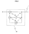
- Fig. 2 is a block diagram illustrating the configuration of the magnitude processing circuit 605 or 606.
- the magnitude processing circuit 606 consists of the coefficient multiplier 691 and the polarity detection circuit 692 each receiving the received signal 1.
- the coefficient multiplier 691 multiplies the input signal, or the received signal 1, by ⁇ .
- the polarity detection circuit 692 outputs 1 when the polarity of the input signal is positive and 0 when the polarity of the input signal is negative.
- the multiplier 693 receives the output of the coefficient multiplier 691 and the output of the polarity detection circuit 692, and outputs the product to the adder 694.
- the adder 694 has the other input terminal receiving the received signal 1 without any change.
- the adder 694 outputs either (1+ ⁇ )x 1 (n) when the polarity of the input signal is positive or x 1 (n) when the polarity of the input signal is negative.
- the magnitude processing circuit 605 outputs either (1+ ⁇ )x 2 (n) when the polarity of the input signal is positive or x 2 (n) when the polarity of the input signal is negative.
- Fig. 3 is a block diagram illustrating the configuration of the delay processing circuit 200.
- the magnitude processing circuit 605 inputs its output signal to one input terminal of the switch 210 and the filter 213 via the input terminal 201.
- the filter 213 filters the signal from the magnitude processing circuit 605 and then inputs the filtered signal to the other input terminal of the switch 210.
- the signal from the magnitude processing circuit 605 and the signal obtained by filtering the signal from the magnitude processing circuit 605 with the filter 213 are respectively supplied to the two input terminals of the switch 210.
- the frequency divider 212 inputs a control signal to the switch 210.
- the control signal is created by frequency-dividing the clock signal from the clock signal generator 211.
- Rectangular pulses with the period equal to the sampling period T of the received signal 2 are generated as the clock signal.
- the clock signal generator 21 is shown in Fig. 3. Actually, it is rare to have a dedicated clock signal generator in the delay processing circuit 200. In this case, a common clock signal to the whole system is supplied to the frequency divider 212 from outside of the delay processing circuit 200. If the frequency divider 212 is a 1/M frequency divider for dividing the frequency of the input signal with a factor of 1/M, the frequency divider 212 alternately outputs a level of "1" and a level of "0" to the switch 210 with a period of MT/2.
- the switch 210 selects the signal from the magnitude processing circuit 605 or the output signal from the filter 213 in synchronous with the leading edge of a rectangular pulse from the frequency divider 212 to transfer it to the output terminal 202.
- the signal delayed by the above-mentioned procedure is output as a pre-processed signal from the output terminal 202.
- Fig. 4A is a block diagram illustrating the configuration of the filter 213.
- an L-tap FIR (Finite Impulse Response) filter is assumed as the filter 213.
- another type of a filter such as an IIR filter may also be used as the filter 213.
- the intput terminal 2130 receives the output signal from the magnitude processing circuit 605 of Fig. 1.
- the signal of the output terminal 2134 is supplied to the switch 210 of Fig. 3.
- the signal of the input terminal 2130 is input to the delay element 2131 1 and the coefficient multiplier 2132 0 .
- Each of delay elements 2131 1 , 2131 2 , ⁇ , 2131 L-1 is a unit delay element for delaying the input signal by one sample.
- the delay elements are connected in a cascade form to construct a tapped delay line with L taps.
- the coefficient multipliers 2132 0 , 2132 1 , ⁇ , 2132 L-1 have coefficients c 0 , c 1 , ⁇ , c L-1 , respectively.
- L 2
- c 0 0
- c 1 1
- the filter 213, for example consists of only the delay element 2131 1 , as shown in Fig. 4B.
- M 1, that is, for the case where the frequency divider 212 of Fig. 1 does not divide the frequency
- the embodiment of the present invention shown in Fig. 4B is equivalent to the method disclosed in the Technical Report of the Institute of Electronics, Information and Communication Engineers of Japan, Vol. DSP96-100, 1996, pp. 17-24 (reference 7).
- the reference 7 analytically shows that the adaptive filter coefficients are uniquely determined.
- the LMS algorithm is disclosed in the "Adaptive Signal Processing” , 1985, pp. 99-113, Prentice-Hall Inc., USA (hereinafter referred to as reference 8) and the normalized LMS (NLMS) algorithm is disclosed in "Adaptive Filters” , 1985, pp. 49-56, Kulwer Academic Publications, USA (hereinafter referred to as reference 9). It is now assumed that the adaptive filters 121 and 122 are controlled using the LMS algorithm with the same step sizes.
- Fig. 5 is a block diagram illustrating the delay processing circuit 200 with the second configuration.
- the second configuration differs from the first configuration of Fig. 3 in that the delay processing circuit 200 has the analysis circuit 221 and the AND circuit 220, in addition to the frequency divider 212.
- the switch 210 changes its status every M samples.
- the switch 210 changes its status according to the logical product of the output signal of the frequency divider 212 and the output signal from the analysis circuit 221.
- the analysis circuit 221 analyzes the output signal from the magnitude processing circuit 605.
- the analysis circuit 221 produces 1 when the analyzed result satisfies a predetermined condition and produces "0" when the analyzed result does not satisfy the predetermined condition, then, outputting it to the AND circuit 220.
- the frequency divider 212 supplies a control signal "0" or "1" to the AND circuit 220.
- the AND circuit 220 detects that the outputs from the analysis circuit 221 and the frequency divider 212 are identical, i.e. the time information coincides with a period of M samples and the analysis results of the input satisfy the predetermined condition simultaneously, and then outputs the signal to control the switching of the switch 210.
- Various methods may be considered to analyze the output of the magnitude processing circuit 605 with the analysis circuit 221. For example, upon focusing on the suppression of subjective noises due to signal discontinuity, variations in magnitude of the output signal of the magnitude processing circuit 605 may be detected.
- Fig. 6 shows the analysis circuit according to the first embodiment.
- the analysis circuit 221 consists of a delay element 2210, a subtracter 2211, an absolute value circuit 2212, a decision circuit 2213, and a memory 2214.
- the delay element 2210 and the subtracter 2211 receive the output signal from the magnitude processing circuit 605, that is, the input signal to the analysis circuit 221.
- the delay element 2210 delays the input signal by one sample period and then outputs the delayed signal to the subtracter 2211.
- the subtracter 2211 subtracts the output signal of the delay element 2210 from the output signal of the magnitude processing circuit 605 and then outputs the difference to the absolute value circuit 2212.
- the absolute value circuit 2212 obtains the absolute value of its input and outputs the result to the decision circuit 2213.
- the memory 2214 supplies a threshold value ⁇ to the decision circuit 2213.
- the decision circuit 2213 outputs "1" when the signal from the absolute value circuit 2212 is smaller than the threshold value and otherwise outputs "0" .
- the decision circuit 2213 outputs its output to the AND circuit 220 of Fig. 5. Namely, when variations in magnitude of the output signal of the magnitude processing circuit 605 are small, the switch 210 changes its status.
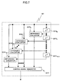
- Fig. 7 shows the analysis circuit 221 based on a post masking, according to the second embodiment.
- the post masking is a phenomenon in which signal samples with a small magnitude following a certain signal sample cannot be perceived by a human' s ear. Post masking is described in detail in "Pcychoacoustics" by Zwicker, translated by Yamada, published by Nishmura Syoten, 1992, pp. 132-146 (reference 10).
- the analysis circuit 221 consists of a group of delay elements 2215 0 , 2215 1 , ⁇ , 2215 N-1 , a group of difference evaluation circuits 2216 0 , 2216 1 , ⁇ , 2216 N-1 , and a control signal generator 2217.
- N is a positive integer.
- the magnitude processing circuit 605 outputs its output signal to the delay element 2215 0 and the difference evaluation circuit 2216 0 .
- Delay elements 2215 0 , 2215 1 , ⁇ , 2215 N-1 form a tapped delay line which delays the supplied signal by one sample period.
- the difference evaluation circuit 2216 0 evaluates the difference between the output signal from the magnitude processing circuit 605 and the signal supplied from the delay element 2215 0 and outputs the result to the control signal generator 2217. Difference evaluation can be performed by subtracting the output signal from the magnitude processing circuit 605 from the signal supplied from the delay element 2215 0 .
- each of the difference evaluation circuits 2216 0 , 2216 1 , ⁇ , 2216 N-1 evaluates the difference between the signal supplied from the corresponding delay element and the output signal from the magnitude processing circuit 605 and then outputs the result to the control signal generator 2217.
- the control signal generator 2217 creates a control signal using evaluation results of difference supplied from the difference evaluation circuits.
- the control signal for example, can be created based on a coincidence among the input signals from the difference evaluation circuits. That is, "1" is output for a coincidence while "0" is output for a non-coincidence.
- the majority of signals from the differential evaluation circuits may be used as a control signal. When “1" holds the majority, "1" is output.
- the reference 10 discloses pre-masking as a similar phenomenon to post masking.
- Pre-masking is a phenomenon in which signals with a small magnitude are masked by signals consecutive thereto, thus, are inaudible by a human' s ear.
- the whole samples of the signal must be delayed. That is, delay elements must be inserted in the two input paths for the switch 210 shown in Fig. 5.
- delay elements with a corresponding delay amount are inserted in the path for the received signal 1 before the adaptive filters 121 and 123 to adjust the delay of the received signal 1.
- the delay amounts of the delay elements depend on the time required for pre-masking detection.
- the switch 210 changes immediately its state before the magnitude of the output signal of the magnitude processing circuit 605 increases.
- the switch 210 cannot change its state. That is, the switching period of the switch 210 is limited to an integer multiple of M.
- the delay processing circuit 200 may be constructed such that the switching period of the switch 210 is not limited to an integer multiple of M.
- Fig. 8 is a block diagram illustrating the delay processing circuit 200 with the third configuration. This configuration differs from the second configuration of Fig. 5 in that a new analysis circuit 222 is added instead of the frequency divider 212, the analysis circuit 221 and the AND circuit 220.
- the switch 210 is controlled by the logical AND between the output of the frequency divider 212 and the output of the analysis circuit 221.
- the analysis circuit 222 analyzes the output signal of the magnitude processing circuit 605 and then directly creates a control signal for the switch 210 using the analysis result and rectangular pulses. The rectangular pulses are supplied from the clock generation circuit 211 to the analysis circuit 222.
- the analysis circuit 222 performs basically the same analysis as the analysis circuit 221.
- the analysis circuit 222 can detect a variance in magnitude of the output signal from the magnitude processing circuit 605 or can perform analysis based on the pre/post masking.
- M 2 T a predetermined sampling period
- the analysis circuit 222 outputs a control signal of "1".
- M 2 is a positive integer satisfying M 2 > 1. In other cases, the analysis circuit 222 outputs a control signal of "0" .
- the analysis circuit 222 outputs the control signal to the switch 210 to control the switching thereof.
- the sampling period is evaluated by counting the rectangular pulses with a counter and then comparing the count with the value M 2 stored in a memory. If the count is equal to the value M 2 , it is judged that the sampling period (M 2 T) has passed. Thus, the analysis circuit 222 outputs "1" while the counter is reset.
- the delay process circuit 200 without the switch 210 in Fig. 2, 5 or 8 may be used instead by suitably setting the coefficients c 0 (k) and c 1 (k).
- Fig. 9 is a block diagram illustrating the delay processing circuit 200 with the fourth configuration.
- the filter 230 receives the received signal 2 via the input terminal 201.
- the filter 230 filters the received signal 2 and outputs the filtered signal to the output terminal 202.
- the clock generation circuit 211 and the frequency divider 212 respectively input control signals to the filter 230.
- the clock generation circuit 211 generates rectangular pulses of a period equal to the sampling period T of the received signal 2.
- the frequency divider 212 supplies the control signal obtained by frequency-dividing the clock from the clock generation circuit 211.
- the filter 230 controls the time-varying coefficient based on the control signals.
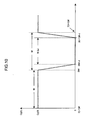
- c 0 (k) is shown in Fig. 10.
- c o (k) takes c o (0) and 0 alternately with a period of 2MT. Strictly, only the first JT and the last JT in a zero-valued range the value of c 0 (k) directly changes from c 0 (0) to 0 or from 0 to c 0 (0). Since c 1 (k) is given by the equation (10), either c 0 (k) or c 1 (k) is zero while the other is non-zero, almost over the whole period of time. That is, c 0 (k) and c 1 (k) are exclusive to each other. A similar switching operation to that of the switch 210 can be executed without the switch 210 of Fig. 3.
- L ⁇ 2 corresponds to taps of the filter 230 connected in parallel.
- c 0 (k) and c 1 (k), c 2 (k), ⁇ , c L-1 (k) are exclusive to each other. When one coefficient is zero, the other coefficients become non-zero.
- c 1 (k), c 2 (k), ⁇ , c L-1 (k) and the corresponding vale of J may respectively have a different value.
- Fig. 11 is a block diagram illustrating the delay processing circuit 200 with the fifth configuration.
- the filter 203 receives the output signal of the magnitude processing circuit 605 input via the input terminal 201.
- the filter 203 filters the output signal from the magnitude processing circuit 605 and then outputs the filtered signal to the output terminal 202.
- the filter 230 also receives the control signals from the clock generation circuit 211 and the AND circuit 220.
- the AND circuit 220 receives the signal from the analysis circuit 211 and the signal from the frequency divider 212.
- the clock generation circuit 211 generates rectangular pulses with a period equal to the sampling period T of the output signal from the magnitude processing circuit 605.
- the frequency divider 212 supplies a control signal to the AND circuit 220.
- the control signal is created by frequency-dividing the clock from the clock generation circuit 211.
- the analysis circuit 221 analyzes the output of the magnitude processing circuit 605 and then outputs "1" to the AND circuit 220 when the result of the analysis satisfies a predetermined condition and "0" to the AND circuit 220 when the result of the analysis does not satisfy the predetermined condition.
- the AND circuit 220 receives a control signal of "0" or 1 from the frequency divider 212.
- the AND circuit 220 detects that the output of the analysis circuit 221 is identical to the output of the frequency divider 212. That is, the time information coincides with the M sample periods and the analysis result on the input signal satisfies the predetermined conditions. Then, the AND circuit 220 outputs its output signal to the filter 230.
- the filter 230 controls the time-varying coefficients based on the control signals.
- Fig. 12 is a block diagram illustrating the delay processing circuit 200 with the sixth configuration.
- This configuration differs from the fifth configuration (described with Fig. 1) in that a new analysis circuit 222 is added instead of the frequency divider 212, the analysis circuit 221 and the AND circuit 220. That is, in the configuration of Fig. 11, the time-varying coefficients of the filter 230 are controlled by the logical AND between the output signals of the frequency divider 212 and the analysis circuit 221. However, in the configuration of Fig. 12, the analysis circuit 222 analyzes the output signal of the magnitude processing circuit 605. Then, the control signals for the filter 230 are directly created using the analysis result and the rectangular pulses supplied from the clock signal generation circuit 211 to the analysis circuit 222.
- the pre-processing circuit 500 which has the delay processing circuit 200 receiving the received signal 2, has been described by referring to Fig. 1.
- the pre-processing circuit 500 may have the delay processing circuit 200 which receives the received signal 1.
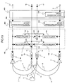
- Fig. 13 shows a multi-channel echo canceller with two channels for the received signals and two channels for the transmission signals, according to the second embodiment of the present invention.
- the second embodiment differs from the first embodiment of Fig. 1 in that the pre-processing circuit 500 and the non-linear process circuit 600 are exchanged in the order. As described earlier, the pre-processing and the non-linear processing are independently applied. Hence, the configuration in which the order of these processings is exchanged can provide similar effects.
- Fig. 14 shows a multi-channel echo canceller with two channels for the received signals and two channels for the transmission signals, according to the third embodiment of the present invention.
- the third embodiment differs from the first embodiment of Fig. 1 in that the non-linear processing circuit 601 is substituted with the non-linear processing circuit 600.
- the non-linear processing circuit 610 includes the magnitude processing circuits 607 and 608 each having the same configuration. Hence, the difference between the non-linear processing circuits 600 and 601 is the difference between magnitude processing circuits 605 and 607.
- Fig. 15 is a block diagram illustrating the configuration of the magnitude processing circuit 607 or 608. This configuration differs from that of the magnitude processing circuit 605 or 606 of Fig. 2 in that the coefficient multiplier 691 receives the received signal 2 instead of the received signal 1.
- the adder 694 produces (x 1 (n) + ⁇ x 2 (n)) for the n-th sample of the received signal when the polarity of the n-th received signal sample x 1 (n) is positive and produces x 1 (n) when the polarity of the n-th received signal sample x 1 (n) is negative.
- the produced signal becomes the output signal of the magnitude processing circuit 608.
- the magnitude processing circuit 607 produces (x 2 (n) + ⁇ x 1 (n)) when the polarity of the input signal is positive and produces x 2 (n) when the polarity of the input signal is negative.
- the other channel since the other channel is used for non-linear processing, the variation from the original signal becomes large. Hence, reduction of the correlation between the channels can be large.
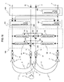
- Fig. 16 shows a multi-channel echo canceller with two channels for the received signals and two channels for the transmission signals according to the fourth embodiment of the present invention.
- the pre-processing circuit 500 and the non-linear processing circuit 610 are exchanged in the order in the third embodiment of Fig. 14. Because of the same reason as that in the second embodiment, the fourth embodiment has effects identical to those by the third embodiment of Fig. 14.
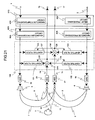
- Fig. 17 shows a multi-channel echo canceller with two channels for the received signals and two channels for the transmission signals according to the fifth embodiment of the present invention.
- the delay processing circuit 605 delays the received signal 2 for the adaptive filters 122 and 124 and the magnitude compensating circuit 606 compensates the amplitude of the received signal 1 for the adaptive filters 121 and 123.
- the delay processing circuit 300 processes the output signal of the magnitude processing circuit 605 to converge the coefficients to correct values.
- the magnitude compensating circuit 400 corrects the magnitude of the output signal of the magnitude processing circuit 606 to compensate the shift of the acoustic image in the acoustic space caused by the delay processing of the delay processing circuit 300.
- the delay processing circuit 300 corrects the magnitude of the output signal of the magnitude processing circuit 605 whenever the magnitude compensating circuit 400 performs magnitude correction.
- the delay processing circuit 200, the delay processing circuit 300 and the magnitude compensating circuit 400 can be constructed in the configuration shown in Fig. 3, 6, 9, 10, 12 or 13.
- the filter 213 is modified from that of Fig. 4.
- the filter 230 is modified from that of Fig. 4.
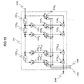
- Fig. 18 is a block diagram illustrating the configuration of the filter 213 containing the delay processing circuit 300 with the configuration of Fig. 3, 6 or 9 and the configuration of the filter 230 containing the delay processing circuit 300 with the configuration of Fig. 9, 12 or 13.
- the filter is an L-tap FIR filter.
- the filter may be in another type such as an IIR filter.
- the coefficient multipliers g 1 , g 2 , ⁇ , g L-1 are inserted in cascade to the coefficient multipliers c 0 , c 1 , c 2 , ⁇ , c L-1 , (except c 0 ).
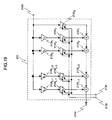
- Fig. 19 is a block diagram illustrating the configuration of the filter 213 having the magnitude compensating circuit 400 with the configuration of Fig. 3, 6 or 9 as well as the configuration of the filter 230 having the magnitude compensating circuit 400 with the configuration of Fig. 9, 12 or 13.
- the filter is an L-tap FIR filter.
- the filter may be in another type such as an IIR filter.
- the delay elements 2132 1 , 2132 2 , ⁇ , 2132 L-1 are not used.
- the two groups correspond to each other.
- the principle of correcting a shift of the acoustic image caused by delay variations by magnitude correction is disclosed in "Medical Research Council Special Report” , No. 166, 1932, pp. 1-32 (reference 11) and "Journal of Acoustical Society of America” , Vol. 32, 1960, pp. 685-692 (reference 12) and "Journal of Acoustical Society of America” , Vol.
- Fig. 20 illustrates another configuration of the filter of Fig. 19.
- a plurality of coefficient multiplier groups each having coefficient multipliers serially connected, are connected in parallel.
- the multiplier groups are integrated into one coefficient multiplier unit.
- the input signal is input to the input terminal 2130.
- the multiplier 2139 with a time varying coefficient c ⁇ multiplies the input signal by c ⁇ .
- the resultant product is output via the output terminal 2134.
- the delay processing circuit 300 applied to the received signal 2 and the magnitude compensating circuit 400 applied to the received signal 1 have been described by referring to Figs. 13, and 18 to 20. However, a similar description can be apparently applied to the delay processing circuit 300 used for the received signal 1 and the magnitude compensating circuit 400 used for the received signal 2.
- Fig. 21 depicts a multi-channel echo canceller with two channels for the received signals and two channels for the transmission signals, according to the sixth embodiment of the present invention. Like the relationship between Figs. 1 and 13, Fig. 21 shows the configuration where the pre-processing circuit 510 and the non-linear processing circuit 600 in Fig. 17 are exchanged in the order.
- Fig. 22 depicts a multi-channel echo canceller with two channels for the received signals and two channels for the transmission signals, according to the seventh embodiment of the present invention.
- Fig. 22 shows the configuration where the non-linear processing circuit 610 is substituted for the non-linear processing circuit 600 in Fig. 17. The effect is apparent from the relationship between the configuration of Fig. 1 and the configuration of Fig. 14.
- Fig. 23 depicts a multi-channel echo canceller with two channels for the received signals and two channels for the transmission signals, according to the eighth embodiment of the present invention.
- Fig. 23 shows the configuration where the non-linear processing circuit 610 and the pre-processing circuit 510 in Fig. 22 are exchanged in the order. The effect is apparent from the relationship between the configuration of Fig. 14 and the configuration of Fig. 16.
- echo cancellation for multi-channel teleconferencing systems has been discussed.
- a similar discussion can be applied to single-channel, multi-point teleconferencing systems being another application of multi-channel echo cancellation.
- an attenuation and a delay are suitably added to the voice of a talker received by a single microphone such that the talker is localized at a desired position between the loudspeakers used on the receiver side.
- a plurality of such signals corresponding to the number of loudspeakers on the receiving side are created.
- the embodiments of the present invention can be applied without any change.
- the present invention is applicable to the case where plural received signals and a single or plural transmission signals are used.
- the received signal propagates from loudspeakers to a microphone via spatial acoustic paths and the acoustic echo received by the microphone is removed.
- the present invention is applicable to cancel echoes other than acoustic echoes, for example, echoes such as crosstalk.
- finite impulse response filters based on the LMS algorithm are used as the adaptive filters 121, 122, 123 and 124 have been described.
- the present invention can use an arbitrary type of adaptive filters. For example, when the finite impulse response filters based on the NLMS algorithm are used, the filter coefficient updates are expressed by:
- the sequential regression algorithm (SRA) (reference 8) and the RLS algorithm (reference 9) may also be used as the algorithm for adaptive filters.
- Infinite impulse response (IIR) adaptive filters may be used instead of the finite impulse response (FIR) adaptive filters.
- the subband adaptive filters or transform-domain adaptive filters may be used.
- one received signal is filtered to create a supplement signal.
- the adaptive filters are operated using a new received signal obtained by time-multiplexing the supplement signal with the original received signal.
- the adaptive filter operates in response to a signal obtained by multiplexing the original received signal with a new supplement signal.
- the multiplex parameter for the original received signal and the supplement signal is controlled based on the nature of the received signal. Meanwhile, the sound shift caused by the introduction of the supplement signal is canceled by correcting the magnitude of the input signals. Thus, the degradation in sound quality of the audible received signal directly supplied to the loudspeaker is suppressed, so that good sound quality can be maintained. Moreover, the convergence time can be shortened by a synergistic effect regarding the non-linear processing and reduction in correlation between the received signals due to the introduction of the supplement signal.
Landscapes
- Filters That Use Time-Delay Elements (AREA)
- Cable Transmission Systems, Equalization Of Radio And Reduction Of Echo (AREA)
- Telephone Function (AREA)
- Noise Elimination (AREA)
Applications Claiming Priority (2)
| Application Number | Priority Date | Filing Date | Title |
|---|---|---|---|
| JP24802598 | 1998-09-02 | ||
| JP24802598A JP3319403B2 (ja) | 1998-09-02 | 1998-09-02 | 多チャネルエコー除去方法及び装置 |
Publications (3)
| Publication Number | Publication Date |
|---|---|
| EP0984609A2 true EP0984609A2 (de) | 2000-03-08 |
| EP0984609A3 EP0984609A3 (de) | 2003-06-11 |
| EP0984609B1 EP0984609B1 (de) | 2005-08-03 |
Family
ID=17172093
Family Applications (1)
| Application Number | Title | Priority Date | Filing Date |
|---|---|---|---|
| EP99250302A Expired - Lifetime EP0984609B1 (de) | 1998-09-02 | 1999-09-01 | Verfahren und Vorrichtung zur Unterdrückung von Mehrkanalechos |
Country Status (4)
| Country | Link |
|---|---|
| US (1) | US6577731B1 (de) |
| EP (1) | EP0984609B1 (de) |
| JP (1) | JP3319403B2 (de) |
| DE (1) | DE69926451T2 (de) |
Cited By (4)
| Publication number | Priority date | Publication date | Assignee | Title |
|---|---|---|---|---|
| EP1845699A1 (de) * | 2006-04-13 | 2007-10-17 | Fraunhofer-Gesellschaft zur Förderung der angewandten Forschung e.V. | Audiosignaldekorrelator |
| WO2007118583A1 (en) * | 2006-04-13 | 2007-10-25 | Fraunhofer-Gesellschaft zur Förderung der angewandten Forschung e.V. | Audio signal decorrelator |
| CN101854193A (zh) * | 2009-04-03 | 2010-10-06 | 瑞昱半导体股份有限公司 | 回音处理装置与其相关方法 |
| CN107452395A (zh) * | 2017-08-23 | 2017-12-08 | 深圳创维-Rgb电子有限公司 | 一种语音信号回声消除装置及电视机 |
Families Citing this family (14)
| Publication number | Priority date | Publication date | Assignee | Title |
|---|---|---|---|---|
| US6771779B1 (en) * | 2000-09-28 | 2004-08-03 | Telefonaktiebolaget Lm Ericsson (Publ) | System, apparatus, and method for improving speech quality in multi-party devices |
| CN1826797A (zh) * | 2003-05-27 | 2006-08-30 | 皇家飞利浦电子股份有限公司 | 具有回波消除系统的扬声器-麦克风系统和回波消除方法 |
| US7471670B1 (en) * | 2004-01-20 | 2008-12-30 | Marvell International Ltd. | Method and apparatus for reducing echo and crosstalk in a communication system |
| US8370113B2 (en) | 2006-09-29 | 2013-02-05 | Netlogic Microsystems, Inc. | Low-power and low-cost adaptive self-linearization system with fast convergence |
| US8041757B2 (en) | 2006-09-29 | 2011-10-18 | Netlogic Microsystems, Inc. | Low power and low complexity adaptive self-linearization |
| US7917337B2 (en) * | 2006-09-29 | 2011-03-29 | Optichron, Inc. | Adaptive self-linearization with separation filter |
| US8032336B2 (en) * | 2006-09-29 | 2011-10-04 | Netlogic Microsystems, Inc. | Distortion cancellation using adaptive linearization |
| US7693672B2 (en) * | 2006-09-29 | 2010-04-06 | Optichron | Adaptive self-linearization |
| DE102007060707B4 (de) * | 2007-12-17 | 2017-12-07 | Austriamicrosystems Ag | Anordnung zur Detektion einer Bewegung eines Körpers sowie Verfahren zum Betrieb einer solchen Anordnung |
| JP5472642B2 (ja) * | 2008-09-26 | 2014-04-16 | 日本電気株式会社 | 信号処理方法、信号処理装置、および信号処理プログラム |
| US9154635B2 (en) | 2008-09-26 | 2015-10-06 | Nec Corporation | Signal processing method, signal processing device, and signal processing program |
| US9653060B1 (en) * | 2016-02-09 | 2017-05-16 | Amazon Technologies, Inc. | Hybrid reference signal for acoustic echo cancellation |
| US9659555B1 (en) * | 2016-02-09 | 2017-05-23 | Amazon Technologies, Inc. | Multichannel acoustic echo cancellation |
| US10522167B1 (en) * | 2018-02-13 | 2019-12-31 | Amazon Techonlogies, Inc. | Multichannel noise cancellation using deep neural network masking |
Family Cites Families (12)
| Publication number | Priority date | Publication date | Assignee | Title |
|---|---|---|---|---|
| US4268727A (en) * | 1979-03-14 | 1981-05-19 | International Telephone And Telegraph Corporation | Adaptive digital echo cancellation circuit |
| JP2792252B2 (ja) * | 1991-03-14 | 1998-09-03 | 日本電気株式会社 | 多チャンネルエコー除去方法および装置 |
| JP2792311B2 (ja) * | 1992-01-31 | 1998-09-03 | 日本電気株式会社 | 多チャンネルエコー除去方法および装置 |
| JP2508574B2 (ja) * | 1992-11-10 | 1996-06-19 | 日本電気株式会社 | 多チャンネルエコ―除去装置 |
| US5568411A (en) * | 1994-07-25 | 1996-10-22 | National Semiconductor Corporation | Method and apparatus for using polarity-coincidence correlators in LMS adaptive filters |
| US5828756A (en) * | 1994-11-22 | 1998-10-27 | Lucent Technologies Inc. | Stereophonic acoustic echo cancellation using non-linear transformations |
| EP0766446B1 (de) * | 1995-09-26 | 2003-06-11 | Nippon Telegraph And Telephone Corporation | Verfahren und Einrichtung zur mehrkanaligen Kompensation eines akustischen Echos |
| JPH09266456A (ja) * | 1996-03-28 | 1997-10-07 | Mitsubishi Electric Corp | エコーキャンセラ |
| JP2842376B2 (ja) * | 1996-05-22 | 1999-01-06 | 日本電気株式会社 | ハンズフリー電話機 |
| US5896452A (en) * | 1996-05-24 | 1999-04-20 | Motorola, Inc. | Multi-channel echo canceler and method using convolution of two training signals |
| US5856970A (en) * | 1996-08-05 | 1999-01-05 | Motorola, Inc. | Multi-channel echo cancellation method and apparatus |
| US5790658A (en) * | 1996-10-28 | 1998-08-04 | Advanced Micro Devices, Inc. | High performance echo canceller for high speed modem |
-
1998
- 1998-09-02 JP JP24802598A patent/JP3319403B2/ja not_active Expired - Fee Related
-
1999
- 1999-09-01 US US09/388,398 patent/US6577731B1/en not_active Expired - Lifetime
- 1999-09-01 DE DE69926451T patent/DE69926451T2/de not_active Expired - Lifetime
- 1999-09-01 EP EP99250302A patent/EP0984609B1/de not_active Expired - Lifetime
Cited By (6)
| Publication number | Priority date | Publication date | Assignee | Title |
|---|---|---|---|---|
| EP1845699A1 (de) * | 2006-04-13 | 2007-10-17 | Fraunhofer-Gesellschaft zur Förderung der angewandten Forschung e.V. | Audiosignaldekorrelator |
| WO2007118583A1 (en) * | 2006-04-13 | 2007-10-25 | Fraunhofer-Gesellschaft zur Förderung der angewandten Forschung e.V. | Audio signal decorrelator |
| US8538037B2 (en) | 2006-04-13 | 2013-09-17 | Fraunhofer-Gesellschaft Zur Foerderung Der Angewandten Forschung E.V. | Audio signal decorrelator, multi channel audio signal processor, audio signal processor, method for deriving an output audio signal from an input audio signal and computer program |
| CN101854193A (zh) * | 2009-04-03 | 2010-10-06 | 瑞昱半导体股份有限公司 | 回音处理装置与其相关方法 |
| CN101854193B (zh) * | 2009-04-03 | 2013-06-05 | 瑞昱半导体股份有限公司 | 回音处理装置与其相关方法 |
| CN107452395A (zh) * | 2017-08-23 | 2017-12-08 | 深圳创维-Rgb电子有限公司 | 一种语音信号回声消除装置及电视机 |
Also Published As
| Publication number | Publication date |
|---|---|
| US6577731B1 (en) | 2003-06-10 |
| DE69926451T2 (de) | 2006-06-01 |
| DE69926451D1 (de) | 2005-09-08 |
| EP0984609A3 (de) | 2003-06-11 |
| JP3319403B2 (ja) | 2002-09-03 |
| JP2000078061A (ja) | 2000-03-14 |
| EP0984609B1 (de) | 2005-08-03 |
Similar Documents
| Publication | Publication Date | Title |
|---|---|---|
| EP0874514B1 (de) | Verfahren und Vorrichtung zum Kompensieren von Mehrkanalechos | |
| EP0984609B1 (de) | Verfahren und Vorrichtung zur Unterdrückung von Mehrkanalechos | |
| Benesty et al. | Advances in network and acoustic echo cancellation | |
| EP1832104B1 (de) | Audiosystem und verfahren zur akustischen echolöschung | |
| EP0944228B1 (de) | Verfahren und Einrichtung zur mehrkanaligen Kompensation eines akustischen Echos | |
| US6895093B1 (en) | Acoustic echo-cancellation system | |
| EP0709999B1 (de) | Verfahren und Einrichtung zur mehrkanaligen Kompensation eines akustischen Echos | |
| EP0627825B1 (de) | Mehrkanal-Echokompensationsverfahren und Vorrichtung dafür | |
| US9008327B2 (en) | Acoustic multi-channel cancellation | |
| RU2495506C2 (ru) | Устройство и способ расчета параметров управления фильтра эхоподавления и устройство и способ расчета величины задержки | |
| EP1698159B1 (de) | System und verfahren für erweitertes stereo-audio | |
| JP5177820B2 (ja) | 強調された主観的ステレオオーディオのためのシステムと方法 | |
| US20110085656A1 (en) | Method and System for Filtering a Signal and for Providing Echo Cancellation | |
| US9497330B2 (en) | Signal processing method, signal processing device, and signal processing program | |
| US9154635B2 (en) | Signal processing method, signal processing device, and signal processing program | |
| EP0253583B1 (de) | Adaptives digitales Filter | |
| JP2850826B2 (ja) | 多チャネルエコー除去方法及び装置 |
Legal Events
| Date | Code | Title | Description |
|---|---|---|---|
| PUAI | Public reference made under article 153(3) epc to a published international application that has entered the european phase |
Free format text: ORIGINAL CODE: 0009012 |
|
| AK | Designated contracting states |
Kind code of ref document: A2 Designated state(s): AT BE CH CY DE DK ES FI FR GB GR IE IT LI LU MC NL PT SE |
|
| AX | Request for extension of the european patent |
Free format text: AL;LT;LV;MK;RO;SI |
|
| PUAL | Search report despatched |
Free format text: ORIGINAL CODE: 0009013 |
|
| AK | Designated contracting states |
Designated state(s): AT BE CH CY DE DK ES FI FR GB GR IE IT LI LU MC NL PT SE |
|
| AX | Request for extension of the european patent |
Extension state: AL LT LV MK RO SI |
|
| 17P | Request for examination filed |
Effective date: 20030611 |
|
| 17Q | First examination report despatched |
Effective date: 20030722 |
|
| AKX | Designation fees paid |
Designated state(s): DE FR GB |
|
| GRAP | Despatch of communication of intention to grant a patent |
Free format text: ORIGINAL CODE: EPIDOSNIGR1 |
|
| GRAS | Grant fee paid |
Free format text: ORIGINAL CODE: EPIDOSNIGR3 |
|
| GRAA | (expected) grant |
Free format text: ORIGINAL CODE: 0009210 |
|
| AK | Designated contracting states |
Kind code of ref document: B1 Designated state(s): DE FR GB |
|
| REG | Reference to a national code |
Ref country code: GB Ref legal event code: FG4D |
|
| REF | Corresponds to: |
Ref document number: 69926451 Country of ref document: DE Date of ref document: 20050908 Kind code of ref document: P |
|
| ET | Fr: translation filed | ||
| PLBE | No opposition filed within time limit |
Free format text: ORIGINAL CODE: 0009261 |
|
| STAA | Information on the status of an ep patent application or granted ep patent |
Free format text: STATUS: NO OPPOSITION FILED WITHIN TIME LIMIT |
|
| 26N | No opposition filed |
Effective date: 20060504 |
|
| PGFP | Annual fee paid to national office [announced via postgrant information from national office to epo] |
Ref country code: GB Payment date: 20090826 Year of fee payment: 11 |
|
| PGFP | Annual fee paid to national office [announced via postgrant information from national office to epo] |
Ref country code: DE Payment date: 20090827 Year of fee payment: 11 |
|
| PGFP | Annual fee paid to national office [announced via postgrant information from national office to epo] |
Ref country code: FR Payment date: 20091012 Year of fee payment: 11 |
|
| GBPC | Gb: european patent ceased through non-payment of renewal fee |
Effective date: 20100901 |
|
| REG | Reference to a national code |
Ref country code: FR Ref legal event code: ST Effective date: 20110531 |
|
| REG | Reference to a national code |
Ref country code: DE Ref legal event code: R119 Ref document number: 69926451 Country of ref document: DE Effective date: 20110401 |
|
| PG25 | Lapsed in a contracting state [announced via postgrant information from national office to epo] |
Ref country code: FR Free format text: LAPSE BECAUSE OF NON-PAYMENT OF DUE FEES Effective date: 20100930 Ref country code: DE Free format text: LAPSE BECAUSE OF NON-PAYMENT OF DUE FEES Effective date: 20110401 |
|
| PG25 | Lapsed in a contracting state [announced via postgrant information from national office to epo] |
Ref country code: GB Free format text: LAPSE BECAUSE OF NON-PAYMENT OF DUE FEES Effective date: 20100901 |