EP0985334B1 - Adapter für elektronischen bauteile - Google Patents
Adapter für elektronischen bauteile Download PDFInfo
- Publication number
- EP0985334B1 EP0985334B1 EP98920687A EP98920687A EP0985334B1 EP 0985334 B1 EP0985334 B1 EP 0985334B1 EP 98920687 A EP98920687 A EP 98920687A EP 98920687 A EP98920687 A EP 98920687A EP 0985334 B1 EP0985334 B1 EP 0985334B1
- Authority
- EP
- European Patent Office
- Prior art keywords
- male
- contact members
- female
- adapter
- contact
- Prior art date
- Legal status (The legal status is an assumption and is not a legal conclusion. Google has not performed a legal analysis and makes no representation as to the accuracy of the status listed.)
- Expired - Lifetime
Links
- 230000008878 coupling Effects 0.000 claims description 6
- 238000010168 coupling process Methods 0.000 claims description 6
- 238000005859 coupling reaction Methods 0.000 claims description 6
- 238000007667 floating Methods 0.000 claims description 6
- 229910000679 solder Inorganic materials 0.000 claims description 3
- 238000005476 soldering Methods 0.000 claims description 3
- 239000011810 insulating material Substances 0.000 claims 1
- 230000002441 reversible effect Effects 0.000 claims 1
- 238000003780 insertion Methods 0.000 abstract description 8
- 230000037431 insertion Effects 0.000 abstract description 8
- 239000000463 material Substances 0.000 description 7
- 238000003466 welding Methods 0.000 description 6
- 230000007547 defect Effects 0.000 description 4
- 239000011159 matrix material Substances 0.000 description 4
- 238000005516 engineering process Methods 0.000 description 2
- 238000000605 extraction Methods 0.000 description 2
- 238000005461 lubrication Methods 0.000 description 2
- 238000000034 method Methods 0.000 description 2
- 239000008188 pellet Substances 0.000 description 2
- 229910001369 Brass Inorganic materials 0.000 description 1
- RYGMFSIKBFXOCR-UHFFFAOYSA-N Copper Chemical compound [Cu] RYGMFSIKBFXOCR-UHFFFAOYSA-N 0.000 description 1
- 229910000881 Cu alloy Inorganic materials 0.000 description 1
- 239000010951 brass Substances 0.000 description 1
- 239000003795 chemical substances by application Substances 0.000 description 1
- 239000004020 conductor Substances 0.000 description 1
- 229910052802 copper Inorganic materials 0.000 description 1
- 239000010949 copper Substances 0.000 description 1
- 230000001419 dependent effect Effects 0.000 description 1
- 230000000694 effects Effects 0.000 description 1
- PCHJSUWPFVWCPO-UHFFFAOYSA-N gold Chemical compound [Au] PCHJSUWPFVWCPO-UHFFFAOYSA-N 0.000 description 1
- 229910052737 gold Inorganic materials 0.000 description 1
- 239000010931 gold Substances 0.000 description 1
- 238000007689 inspection Methods 0.000 description 1
- 238000009434 installation Methods 0.000 description 1
- 238000012423 maintenance Methods 0.000 description 1
- 230000013011 mating Effects 0.000 description 1
- 230000000750 progressive effect Effects 0.000 description 1
- 238000007650 screen-printing Methods 0.000 description 1
- 238000004381 surface treatment Methods 0.000 description 1
- 239000012780 transparent material Substances 0.000 description 1
- 210000001364 upper extremity Anatomy 0.000 description 1
- 238000011179 visual inspection Methods 0.000 description 1
Images

Classifications
-
- H—ELECTRICITY
- H05—ELECTRIC TECHNIQUES NOT OTHERWISE PROVIDED FOR
- H05K—PRINTED CIRCUITS; CASINGS OR CONSTRUCTIONAL DETAILS OF ELECTRIC APPARATUS; MANUFACTURE OF ASSEMBLAGES OF ELECTRICAL COMPONENTS
- H05K7/00—Constructional details common to different types of electric apparatus
- H05K7/02—Arrangements of circuit components or wiring on supporting structure
- H05K7/10—Plug-in assemblages of components, e.g. IC sockets
- H05K7/1053—Plug-in assemblages of components, e.g. IC sockets having interior leads
- H05K7/1076—Plug-in assemblages of components, e.g. IC sockets having interior leads co-operating by sliding
- H05K7/1084—Plug-in assemblages of components, e.g. IC sockets having interior leads co-operating by sliding pin grid array package carriers
Definitions
- the present invention relates to an adapter or base for installing an electronic component in a way removable on a printed circuit.
- An adapter interposed between a component having pins and a printed circuit is known from WO-A-9116740.
- the adapter is more particularly intended for components using the BGA ball grid array technology.
- BGA components have on their underside a sphere-shaped soldering grid or matrix or portion of a sphere.
- the printed circuit in the area intended to receive the component, comprises a matrix of contact pads corresponding to the grid of spheres of the component.
- adapters including two elements, a first female element whose underside is soldered on the printed circuit and which has a connection element on its upper face female.
- the second element of the adapter has on its upper face a grid of cylindrical pellets on which a BGA type component can be soldered.
- the face bottom of the male element comprises means for male connection.
- the object of the present invention is to remedy the disadvantages mentioned above by offering an adapter which guarantees good electrical connections and which reduces the force required to be applied to the component to make the connection during coupling of its male and female parts.
- the adapter according the invention is distinguished for this purpose by the characteristics defined in claim 1.
- the adapter object of the present invention allows in addition to easily checking the condition of the welds without requiring the implementation of an X-ray device.
- Figure 1 is a perspective view of an adapter for electronic components according to the present invention.
- Figure 2 is a side view of the male part of the adapter illustrated in figure 1.
- Figure 3 is a side view of the female part of the adapter shown in Figure 1.
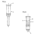
- Figure 4 is a side view of an element of male contact to be implanted in the body of the male part of the adapter.
- Figure 5 is a partial sectional view of a female contact element to be implanted in the body of the female part of the adapter.
- the adapter includes two separate parts, a first male part 1 intended to receive the electronic component (not shown), and a second female part 2 intended to be welded to a printed circuit (not shown).
- the male part 1 is consisting of a body 3 made of a plastic material insulating.
- the upper face of the male part 1 has a matrix or grid of cylindrical pellets 4. These cylindrical pads 4 correspond in their alignment and their configuration to the spheres or portion of solder spheres found on the underside of an electronic component of BGA technology. It is thus possible to solder the electronic component on the upper side of the body 3.
- Male contact elements 5.6 are implanted in body 3.
- the upper extremity of each of the male contact elements 5 is in contact with the corresponding tablet 4.
- the lower female part 2 of the adapter is also consisting of a body 7 made of a material dielectric plastic identical to that of body 3. It has on its underside a grid or matrix of spheres or portion of spheres 9 in contact with female contact elements 8 implanted in the body 7.
- the underside of the female part is welded to the corresponding pads of a printed circuit.
- the elements contact contacts 8 are mounted floating in the body 7.
- the floating game is, as for the part male, between 50 and 100 microns, preferably 75 microns.
- This material in addition to its dielectric characteristics must also resist without deformation and without altering its transparency to temperatures higher than those encountered during component welding operations.
- a material such as GRILAMID TR 70, sold by the company EMS-CHEMIE AG is perfectly adapted.
- the use of a transparent material, and which remains transparent after welding operation, for making the adapter body allows visual inspection of welds made. Using a simple microscope, it is easy to check the condition of the welds and more particularly detect the presence of short circuits. Thanks to this feature, avoiding the use of expensive equipment such as an x-ray inspection device to perform these control operations.
- Figure 2 shows that some of the elements of male contact 6, in particular those located in the part center of the adapter edge, have a shorter length than that of the contact elements male 5 located in the corners of the adapter.
- FIG 3 shows, however, that the elements of female contact 8 all have similar dimensions.
- FIG. 4 illustrates a possible embodiment among many variants of a male contact element 5.6.
- This contact element has an upper part implanted in the body 3 of the adapter and a part lower intended to cooperate with the contact element female to establish the connection.
- the upper portion male contact elements constitutes the cylindrical plate 4 which emerges from the body 3 to receive the component electronic by welding.
- These male contact elements are made of a conductive material such as copper or an alloy of copper and brass. They can also be plated with a thin layer of gold for example.
- FIG. 3 illustrates a female contact element 8 intended to be implanted in the body 7 of the female element 2 of the adapter.
- This female contact element 8 is in the form of a hollow cylindrical body, closed at its lower end by a weld sphere 9. Inside this body is arranged a clip of support 10 having substantially the same diameter as the body in its upper part, and shrinking in its lower part. This clip allows you to receive the protruding part of the male contact element 5,6 and the keep in service position after coupling performed.
- These conventional type clips 10 can have several lips or longitudinal slits 11 which deviate during the introduction of the male contact 5.6. They are also made of a material ensuring good conductivity and may have a surface treatment facilitating the introduction of the male element into the element female.
- An example is a lubrication of the emerging part outside the body of the elements male contacts, as well as from the inside of the female contact (8) or clips (10) fitted to them.
- This lubrication can be obtained by different methods such than filing by screen printing or any other process known.
- the adapter according to the invention comprises elements contact male 5.6 which have at least two different lengths. These male contact elements 5,6 cooperate with the female contact elements 8 during the connection. It will be noted that the female contact elements 8 all have the same dimensions. this allows to establish two successive levels of contact. Like this shown in Figures 1 and 2, some contact elements male 5 have a first length to establish a first level of contact, the other contact elements male 6 have a second, shorter length, for establish a second level of contact.
- the introduction of the male part into the part female is done gradually. Initially time, only the male contact elements 5, having the longest length, contact and move the clips 10 apart from the female contact elements 8 corresponding. Once these are in place, the elements of male contact 6 of shorter length deviate to in turn the clips 10 of the female contact elements 8.
- the force required for insertion is thus divided into two step. In order to obtain an adequate distribution of the force to apply, a percentage between 30% and 45%, preferably 37% of the male contact elements have the shortest length.
- the contact elements male 5 longest will be distributed on the periphery external of the contact grid.
- the difference of length between first level contact elements 5 and the second level contact elements 6 is about 350 microns.
- the difference of length between the male contact elements 5 allowing to establish the first level of contact and the elements of male contact 6 for establishing the second contact level is between 3% and 25%, preferably between 8% and 14% of the length of a male contact element 5.
- part of the elements contact socket 8 includes clips 10 arranged at a first distance from the insertion opening, a second part of the female contact elements 8 comprising clips 10 arranged at a second, larger distance, from the insertion hole. It goes without saying that this function can be achieved by combining elements of male contact 5,6 having different lengths and female contact elements 8 provided with clips 10 arranged at different distances from the opening through which the male contact element penetrates. In this way, by cumulating both characteristics, we get at least four levels of contact during mating.
Landscapes
- Engineering & Computer Science (AREA)
- Microelectronics & Electronic Packaging (AREA)
- Coupling Device And Connection With Printed Circuit (AREA)
- Details Of Connecting Devices For Male And Female Coupling (AREA)
- Fixed Capacitors And Capacitor Manufacturing Machines (AREA)
- Telephone Function (AREA)
- Connecting Device With Holders (AREA)
Claims (10)
- Adapter, ein elektronisches Bauteil auswechselbar auf eine gedruckte Schaltung aufzustecken erlaubend, mit einem ersten Teilstück, das auf seiner Unterseite Mittel (9) aufweist, die gestatten, es auf eine gedruckte Schaltung aufzulöten, und einem zweiten Teilstück, dessen Oberseite mit Mitteln (4) versehen ist, die dazu geeignet sind, durch Lötverbindung ein elektronisches Bauteil aufzunehmen, wobei eines der benannten Teilstücke (1) einen Körper (3) umfasst, der mit einer Mehrzahl von Kontaktstiftelementen (5, 6) versehen ist, und das andere Teilstück (2) einen Körper (7) umfasst, der mit entsprechenden Kontakthülsenelementen (8) versehen ist, die dafür bestimmt sind, mit den Kontaktstiftelementen (5, 6) zusammenzuwirken, um eine Verbindung zwischen dem elektronischen Bauteil und der gedruckten Schaltung herzustellen, dadurch gekennzeichnet, dass die Kontaktelemente (5, 6, 8) so gestaltet sind, dass zumindest zwei aufeinanderfolgende Kontaktebenen hergestellt werden, wenn das erste an das zweite Teilstück angekoppelt wird.
- Adapter nach Anspruch 1, dadurch gekennzeichnet, dass ein erster Teil der Kontaktstiftelemente (5) eine erste Länge aufweist, die es gestattet, eine erste Kontaktebene herzustellen, und dass ein zweiter Teil der Kontaktstiftelemente (6) eine zweite, geringere Länge aufweist, um eine zweite Kontaktebene herzustellen.
- Adapter nach Anspruch 1, dadurch gekennzeichnet, dass die Kontakthülsenelemente (8) Klemmen (10) umfassen, die dazu bestimmt sind, die entsprechenden Kontaktstiftelemente zu empfangen, und dadurch, dass ein erster Teil der Kontakthülsenelemente (8) Klemmen (10) umfasst, die bei einem ersten Abstand zur Eintrittsöffnung angeordnet sind, während ein zweiter Teil der Kontakthülsenelemente (8) Klemmen (10) umfasst, die bei einem zweiten, grösseren Abstand von der benannten Eintrittsöffnung angeordnet sind, um zumindest zwei aufeinanderfolgende Kontaktebenen herzustellen.
- Adapter nach einem der vorangehenden Ansprüche, dadurch gekennzeichnet, dass der Anteil der die erste, grössere Länge aufweisenden Kontaktstiftelemente (5) zwischen 55 % und 70 % der Gesamtzahl, bevorzugt bei 63 % liegt.
- Adapter nach einem der vorangehenden Ansprüche, dadurch gekennzeichnet, dass die Kontaktelemente (5, 8), die die erste Kontaktebene herzustellen gestatten, auf der Peripherie des Adapters verteilt sind.
- Adapter nach einem der vorangehenden Ansprüche, dadurch gekennzeichnet, dass die Kontaktelemente (6, 8), die die zweite Kontaktebene herzustellen gestatten, im mittleren Teil der Seiten der Körper (3, 7) des Adapters angeordnet sind.
- Adapter nach einem der vorangehenden Ansprüche, dadurch gekennzeichnet, dass der Längenunterschied zwischen den Kontaktstifielementen, die die erste Kontaktebene (5) herzustellen gestatten, und den Kontaktstiftelementen (6), die die zweite Kontaktebene herzustellen gestatten, zwischen 3 % und 25 %, vorzugsweise zwischen 8 % und 14 % der Länge eines Kontaktstifts (5) liegt.
- Adapter nach einem der vorangehenden Ansprüche, dadurch gekennzeichnet, dass die Kontaktstift- (5, 6) und -hülsenelemente (8) im Körper (3, 7) des Steck- (1) bzw. Hülsenteilstücks (2) des Adapters federnd eingesetzt sind, wobei das Arbeitsspiel auf Werte zwischen 50 und 100 µm und vorzugsweise auf 75 µm begrenzt ist.
- Adapter nach einem der vorangehenden Ansprüche, dadurch gekennzeichnet, dass die Körper (3, 7) der beiden Adapterteilstücke aus einem durchsichtigen isolierenden Material gefertigt sind.
- Adapter nach einem der vorangehenden Ansprüche, dadurch gekennzeichnet, dass die Kontaktstift- (5, 6) und -hülsenelemente (8) geschmiert sind, um das Ankoppeln des Stift- (1) und Hülsenteilstücks (2) des Adapters zu begünstigen.
Applications Claiming Priority (3)
| Application Number | Priority Date | Filing Date | Title |
|---|---|---|---|
| CH127797 | 1997-05-30 | ||
| CH01277/97A CH691561A5 (fr) | 1997-05-30 | 1997-05-30 | Adapteur pour composants électroniques. |
| PCT/IB1998/000829 WO1998054937A1 (fr) | 1997-05-30 | 1998-05-28 | Adaptateur pour composants electroniques |
Publications (2)
| Publication Number | Publication Date |
|---|---|
| EP0985334A1 EP0985334A1 (de) | 2000-03-15 |
| EP0985334B1 true EP0985334B1 (de) | 2001-08-01 |
Family
ID=4206663
Family Applications (1)
| Application Number | Title | Priority Date | Filing Date |
|---|---|---|---|
| EP98920687A Expired - Lifetime EP0985334B1 (de) | 1997-05-30 | 1998-05-28 | Adapter für elektronischen bauteile |
Country Status (9)
| Country | Link |
|---|---|
| US (1) | US6334780B1 (de) |
| EP (1) | EP0985334B1 (de) |
| JP (1) | JP2002507312A (de) |
| CN (1) | CN1139310C (de) |
| AT (1) | ATE203871T1 (de) |
| AU (1) | AU7347198A (de) |
| CH (1) | CH691561A5 (de) |
| DE (1) | DE69801282T2 (de) |
| WO (1) | WO1998054937A1 (de) |
Cited By (1)
| Publication number | Priority date | Publication date | Assignee | Title |
|---|---|---|---|---|
| EP2173019A1 (de) | 2008-10-01 | 2010-04-07 | Valeo Equipements Electriques Moteur | Stator einer elektrisch umlaufenden Maschine |
Families Citing this family (3)
| Publication number | Priority date | Publication date | Assignee | Title |
|---|---|---|---|---|
| DE202005010927U1 (de) * | 2005-07-12 | 2006-11-16 | Cooper Crouse-Hinds Gmbh | Explosionsgeschützter Steckverbinder |
| JP5077542B2 (ja) * | 2007-09-06 | 2012-11-21 | 日本電気株式会社 | 電子部品パッケージの位置調整ユニット |
| JP5574778B2 (ja) * | 2010-03-26 | 2014-08-20 | Juki株式会社 | 部品実装装置 |
Family Cites Families (9)
| Publication number | Priority date | Publication date | Assignee | Title |
|---|---|---|---|---|
| WO1991016740A1 (en) | 1990-04-16 | 1991-10-31 | Mckenzie Socket Technology, Inc. | Intermediary adapter-connector |
| US5046972A (en) * | 1990-07-11 | 1991-09-10 | Amp Incorporated | Low insertion force connector and contact |
| US5232382A (en) * | 1992-08-28 | 1993-08-03 | Foxconn International, Inc. | PGA socket contact |
| US5384492A (en) * | 1992-11-20 | 1995-01-24 | Unisys Corporation | Protective system for insertion/extraction of PC boards in a powered-up environment |
| KR987001149A (ko) * | 1995-10-31 | 1998-04-30 | 오오우라 히로시 | 볼.그리드.어레이 반도체 측정용 소켓 |
| US5730606A (en) * | 1996-04-02 | 1998-03-24 | Aries Electronics, Inc. | Universal production ball grid array socket |
| US6007348A (en) * | 1996-05-07 | 1999-12-28 | Advanced Intercommunications Corporation | Solder ball terminal |
| US5982635A (en) * | 1996-10-23 | 1999-11-09 | Concept Manufacturing, Incorporated | Signal adaptor board for a pin grid array |
| AU6337998A (en) * | 1997-02-28 | 1998-09-18 | Cornell Research Foundation Inc. | Self-assembled low-insertion force connector assembly |
-
1997
- 1997-05-30 CH CH01277/97A patent/CH691561A5/fr not_active IP Right Cessation
-
1998
- 1998-05-28 DE DE69801282T patent/DE69801282T2/de not_active Expired - Fee Related
- 1998-05-28 CN CNB988056496A patent/CN1139310C/zh not_active Expired - Fee Related
- 1998-05-28 EP EP98920687A patent/EP0985334B1/de not_active Expired - Lifetime
- 1998-05-28 WO PCT/IB1998/000829 patent/WO1998054937A1/fr not_active Ceased
- 1998-05-28 US US09/424,765 patent/US6334780B1/en not_active Expired - Fee Related
- 1998-05-28 JP JP55077298A patent/JP2002507312A/ja active Pending
- 1998-05-28 AT AT98920687T patent/ATE203871T1/de not_active IP Right Cessation
- 1998-05-28 AU AU73471/98A patent/AU7347198A/en not_active Abandoned
Cited By (1)
| Publication number | Priority date | Publication date | Assignee | Title |
|---|---|---|---|---|
| EP2173019A1 (de) | 2008-10-01 | 2010-04-07 | Valeo Equipements Electriques Moteur | Stator einer elektrisch umlaufenden Maschine |
Also Published As
| Publication number | Publication date |
|---|---|
| DE69801282D1 (de) | 2001-09-06 |
| HK1026566A1 (en) | 2000-12-15 |
| CH691561A5 (fr) | 2001-08-15 |
| EP0985334A1 (de) | 2000-03-15 |
| CN1258430A (zh) | 2000-06-28 |
| CN1139310C (zh) | 2004-02-18 |
| AU7347198A (en) | 1998-12-30 |
| US6334780B1 (en) | 2002-01-01 |
| DE69801282T2 (de) | 2002-05-08 |
| WO1998054937A1 (fr) | 1998-12-03 |
| ATE203871T1 (de) | 2001-08-15 |
| JP2002507312A (ja) | 2002-03-05 |
Similar Documents
| Publication | Publication Date | Title |
|---|---|---|
| EP0838878A1 (de) | Federkontaktelement | |
| CH693478A5 (fr) | Socle de connexion de deux composants électriques. | |
| WO1998006063A1 (fr) | Carte a circuit integre a connexion mixte | |
| FR2826230A1 (fr) | Dispositif et procede de fixation de circuits integres sur une carte a circuit imprime | |
| EP0545790B1 (de) | Elektrische Verbindungsvorrichtung | |
| FR2949171A1 (fr) | Procede d'assemblage de deux composants electroniques | |
| EP0717442B1 (de) | Träger für integrierten Schaltkreis zur Kontaktierung eines anderen Trägers mittels Kontaktkugeln | |
| FR2853997A1 (fr) | Piece de contact pour connecteur electrique | |
| EP0985334A1 (de) | Adapter für elektronischen bauteile | |
| EP2693468B1 (de) | Verfahren vom Typ Flip-Chip zum Zusammenbauen zweier elektronischer Bauteile | |
| FR2683397A1 (fr) | Douille electrique pour interconnecter des circuits sur une puce et des circuits sur un substrat. | |
| FR2753819A1 (fr) | Carte a circuit integre a connexion mixte | |
| WO2018033689A1 (fr) | Procédé de connection intercomposants à densité optimisée | |
| FR2965139A1 (fr) | Support de circuit et procede de fabrication d'un tel support de circuit | |
| FR2706139A1 (fr) | Matériau pour brasure. | |
| EP1764828A1 (de) | Verbinden zweier Bauteile mittels Lothöckern unterschiedlicher Grösse und derartig hergestellte Vorrichtung | |
| FR2814859A1 (fr) | Dispositif et procede pour etablir un contact electrique avec une carte de circuit imprime flexible | |
| EP1278240A2 (de) | Verfahren zur Transferierung von einem Bauelement auf einen Verbindungsträger durch Löten ohne zusätzliches Lötmaterial | |
| WO2012143086A1 (fr) | Connecteur a insertion par pression | |
| FR2818870A1 (fr) | Procede de realisation d'interconnexion dans un circuit imprime multicouches | |
| FR2620569A1 (fr) | Procede pour calibrer l'epaisseur d'une soudure d'un composant electronique sur un substrat | |
| FR2862413A1 (fr) | Capteur de mesure a liaisons conductrices sans raideur et procede de fabrication | |
| WO2020094936A1 (fr) | Procédé de liaison par brasage permettant d'améliorer la tenue en fatigue de joints brasés | |
| FR2768897A1 (fr) | Dispositif d'interconnexion de modules electroniques dans un assemblage a trois dimensions | |
| WO2026052506A1 (fr) | Ensemble électrique, notamment pour un onduleur |
Legal Events
| Date | Code | Title | Description |
|---|---|---|---|
| PUAI | Public reference made under article 153(3) epc to a published international application that has entered the european phase |
Free format text: ORIGINAL CODE: 0009012 |
|
| 17P | Request for examination filed |
Effective date: 19991130 |
|
| AK | Designated contracting states |
Kind code of ref document: A1 Designated state(s): AT BE CH CY DE DK ES FI FR GB GR IE IT LI LU MC NL PT SE |
|
| GRAG | Despatch of communication of intention to grant |
Free format text: ORIGINAL CODE: EPIDOS AGRA |
|
| 17Q | First examination report despatched |
Effective date: 20001116 |
|
| GRAG | Despatch of communication of intention to grant |
Free format text: ORIGINAL CODE: EPIDOS AGRA |
|
| GRAH | Despatch of communication of intention to grant a patent |
Free format text: ORIGINAL CODE: EPIDOS IGRA |
|
| GRAH | Despatch of communication of intention to grant a patent |
Free format text: ORIGINAL CODE: EPIDOS IGRA |
|
| GRAA | (expected) grant |
Free format text: ORIGINAL CODE: 0009210 |
|
| AK | Designated contracting states |
Kind code of ref document: B1 Designated state(s): AT BE CH CY DE DK ES FI FR GB GR IE IT LI LU MC NL PT SE |
|
| PG25 | Lapsed in a contracting state [announced via postgrant information from national office to epo] |
Ref country code: NL Free format text: LAPSE BECAUSE OF FAILURE TO SUBMIT A TRANSLATION OF THE DESCRIPTION OR TO PAY THE FEE WITHIN THE PRESCRIBED TIME-LIMIT Effective date: 20010801 Ref country code: FI Free format text: LAPSE BECAUSE OF FAILURE TO SUBMIT A TRANSLATION OF THE DESCRIPTION OR TO PAY THE FEE WITHIN THE PRESCRIBED TIME-LIMIT Effective date: 20010801 Ref country code: AT Free format text: LAPSE BECAUSE OF FAILURE TO SUBMIT A TRANSLATION OF THE DESCRIPTION OR TO PAY THE FEE WITHIN THE PRESCRIBED TIME-LIMIT Effective date: 20010801 |
|
| REF | Corresponds to: |
Ref document number: 203871 Country of ref document: AT Date of ref document: 20010815 Kind code of ref document: T |
|
| REG | Reference to a national code |
Ref country code: CH Ref legal event code: EP |
|
| REG | Reference to a national code |
Ref country code: IE Ref legal event code: FG4D Free format text: FRENCH |
|
| REF | Corresponds to: |
Ref document number: 69801282 Country of ref document: DE Date of ref document: 20010906 |
|
| PG25 | Lapsed in a contracting state [announced via postgrant information from national office to epo] |
Ref country code: DK Free format text: LAPSE BECAUSE OF FAILURE TO SUBMIT A TRANSLATION OF THE DESCRIPTION OR TO PAY THE FEE WITHIN THE PRESCRIBED TIME-LIMIT Effective date: 20011101 |
|
| PG25 | Lapsed in a contracting state [announced via postgrant information from national office to epo] |
Ref country code: GR Free format text: LAPSE BECAUSE OF FAILURE TO SUBMIT A TRANSLATION OF THE DESCRIPTION OR TO PAY THE FEE WITHIN THE PRESCRIBED TIME-LIMIT Effective date: 20011102 |
|
| PG25 | Lapsed in a contracting state [announced via postgrant information from national office to epo] |
Ref country code: PT Free format text: LAPSE BECAUSE OF FAILURE TO SUBMIT A TRANSLATION OF THE DESCRIPTION OR TO PAY THE FEE WITHIN THE PRESCRIBED TIME-LIMIT Effective date: 20011105 |
|
| REG | Reference to a national code |
Ref country code: CH Ref legal event code: NV Representative=s name: KIRKER & CIE SA |
|
| GBT | Gb: translation of ep patent filed (gb section 77(6)(a)/1977) |
Effective date: 20011102 |
|
| REG | Reference to a national code |
Ref country code: GB Ref legal event code: IF02 |
|
| NLV1 | Nl: lapsed or annulled due to failure to fulfill the requirements of art. 29p and 29m of the patents act | ||
| PG25 | Lapsed in a contracting state [announced via postgrant information from national office to epo] |
Ref country code: ES Free format text: LAPSE BECAUSE OF FAILURE TO SUBMIT A TRANSLATION OF THE DESCRIPTION OR TO PAY THE FEE WITHIN THE PRESCRIBED TIME-LIMIT Effective date: 20020228 |
|
| PG25 | Lapsed in a contracting state [announced via postgrant information from national office to epo] |
Ref country code: MC Free format text: LAPSE BECAUSE OF NON-PAYMENT OF DUE FEES Effective date: 20020528 Ref country code: LU Free format text: LAPSE BECAUSE OF NON-PAYMENT OF DUE FEES Effective date: 20020528 |
|
| PG25 | Lapsed in a contracting state [announced via postgrant information from national office to epo] |
Ref country code: CY Free format text: LAPSE BECAUSE OF FAILURE TO SUBMIT A TRANSLATION OF THE DESCRIPTION OR TO PAY THE FEE WITHIN THE PRESCRIBED TIME-LIMIT Effective date: 20020531 |
|
| PLBE | No opposition filed within time limit |
Free format text: ORIGINAL CODE: 0009261 |
|
| STAA | Information on the status of an ep patent application or granted ep patent |
Free format text: STATUS: NO OPPOSITION FILED WITHIN TIME LIMIT |
|
| 26N | No opposition filed | ||
| PGFP | Annual fee paid to national office [announced via postgrant information from national office to epo] |
Ref country code: GB Payment date: 20040810 Year of fee payment: 7 |
|
| PGFP | Annual fee paid to national office [announced via postgrant information from national office to epo] |
Ref country code: DE Payment date: 20040819 Year of fee payment: 7 |
|
| PGFP | Annual fee paid to national office [announced via postgrant information from national office to epo] |
Ref country code: FR Payment date: 20040820 Year of fee payment: 7 |
|
| PGFP | Annual fee paid to national office [announced via postgrant information from national office to epo] |
Ref country code: SE Payment date: 20040823 Year of fee payment: 7 |
|
| PGFP | Annual fee paid to national office [announced via postgrant information from national office to epo] |
Ref country code: IE Payment date: 20040825 Year of fee payment: 7 |
|
| PGFP | Annual fee paid to national office [announced via postgrant information from national office to epo] |
Ref country code: CH Payment date: 20040827 Year of fee payment: 7 |
|
| PGFP | Annual fee paid to national office [announced via postgrant information from national office to epo] |
Ref country code: BE Payment date: 20040916 Year of fee payment: 7 |
|
| PG25 | Lapsed in a contracting state [announced via postgrant information from national office to epo] |
Ref country code: IT Free format text: LAPSE BECAUSE OF NON-PAYMENT OF DUE FEES Effective date: 20050528 Ref country code: GB Free format text: LAPSE BECAUSE OF NON-PAYMENT OF DUE FEES Effective date: 20050528 |
|
| PG25 | Lapsed in a contracting state [announced via postgrant information from national office to epo] |
Ref country code: SE Free format text: LAPSE BECAUSE OF NON-PAYMENT OF DUE FEES Effective date: 20050529 |
|
| PG25 | Lapsed in a contracting state [announced via postgrant information from national office to epo] |
Ref country code: IE Free format text: LAPSE BECAUSE OF NON-PAYMENT OF DUE FEES Effective date: 20050530 |
|
| PG25 | Lapsed in a contracting state [announced via postgrant information from national office to epo] |
Ref country code: LI Free format text: LAPSE BECAUSE OF NON-PAYMENT OF DUE FEES Effective date: 20050531 Ref country code: CH Free format text: LAPSE BECAUSE OF NON-PAYMENT OF DUE FEES Effective date: 20050531 Ref country code: BE Free format text: LAPSE BECAUSE OF NON-PAYMENT OF DUE FEES Effective date: 20050531 |
|
| BERE | Be: lapsed |
Owner name: S.A. *ULTRA PRECISION HOLDING Effective date: 20050531 |
|
| PG25 | Lapsed in a contracting state [announced via postgrant information from national office to epo] |
Ref country code: DE Free format text: LAPSE BECAUSE OF NON-PAYMENT OF DUE FEES Effective date: 20051201 |
|
| REG | Reference to a national code |
Ref country code: CH Ref legal event code: PL |
|
| EUG | Se: european patent has lapsed | ||
| GBPC | Gb: european patent ceased through non-payment of renewal fee |
Effective date: 20050528 |
|
| PG25 | Lapsed in a contracting state [announced via postgrant information from national office to epo] |
Ref country code: FR Free format text: LAPSE BECAUSE OF NON-PAYMENT OF DUE FEES Effective date: 20060131 |
|
| REG | Reference to a national code |
Ref country code: IE Ref legal event code: MM4A |
|
| REG | Reference to a national code |
Ref country code: FR Ref legal event code: ST Effective date: 20060131 |
|
| BERE | Be: lapsed |
Owner name: S.A. *ULTRA PRECISION HOLDING Effective date: 20050531 |