EP0985977A1 - Analyse von latenten Bildern bei der Herstellung von integrierten Schaltkreisen - Google Patents
Analyse von latenten Bildern bei der Herstellung von integrierten Schaltkreisen Download PDFInfo
- Publication number
- EP0985977A1 EP0985977A1 EP99306919A EP99306919A EP0985977A1 EP 0985977 A1 EP0985977 A1 EP 0985977A1 EP 99306919 A EP99306919 A EP 99306919A EP 99306919 A EP99306919 A EP 99306919A EP 0985977 A1 EP0985977 A1 EP 0985977A1
- Authority
- EP
- European Patent Office
- Prior art keywords
- lithographic
- latent image
- parameter
- order diffraction
- radiation
- Prior art date
- Legal status (The legal status is an assumption and is not a legal conclusion. Google has not performed a legal analysis and makes no representation as to the accuracy of the status listed.)
- Withdrawn
Links
Images



Classifications
-
- G—PHYSICS
- G03—PHOTOGRAPHY; CINEMATOGRAPHY; ANALOGOUS TECHNIQUES USING WAVES OTHER THAN OPTICAL WAVES; ELECTROGRAPHY; HOLOGRAPHY
- G03F—PHOTOMECHANICAL PRODUCTION OF TEXTURED OR PATTERNED SURFACES, e.g. FOR PRINTING, FOR PROCESSING OF SEMICONDUCTOR DEVICES; MATERIALS THEREFOR; ORIGINALS THEREFOR; APPARATUS SPECIALLY ADAPTED THEREFOR
- G03F7/00—Photomechanical, e.g. photolithographic, production of textured or patterned surfaces, e.g. printing surfaces; Materials therefor, e.g. comprising photoresists; Apparatus specially adapted therefor
- G03F7/70—Microphotolithographic exposure; Apparatus therefor
- G03F7/70483—Information management; Active and passive control; Testing; Wafer monitoring, e.g. pattern monitoring
- G03F7/7055—Exposure light control in all parts of the microlithographic apparatus, e.g. pulse length control or light interruption
- G03F7/70558—Dose control, i.e. achievement of a desired dose
-
- H—ELECTRICITY
- H10—SEMICONDUCTOR DEVICES; ELECTRIC SOLID-STATE DEVICES NOT OTHERWISE PROVIDED FOR
- H10P—GENERIC PROCESSES OR APPARATUS FOR THE MANUFACTURE OR TREATMENT OF DEVICES COVERED BY CLASS H10
- H10P76/00—Manufacture or treatment of masks on semiconductor bodies, e.g. by lithography or photolithography
-
- G—PHYSICS
- G03—PHOTOGRAPHY; CINEMATOGRAPHY; ANALOGOUS TECHNIQUES USING WAVES OTHER THAN OPTICAL WAVES; ELECTROGRAPHY; HOLOGRAPHY
- G03F—PHOTOMECHANICAL PRODUCTION OF TEXTURED OR PATTERNED SURFACES, e.g. FOR PRINTING, FOR PROCESSING OF SEMICONDUCTOR DEVICES; MATERIALS THEREFOR; ORIGINALS THEREFOR; APPARATUS SPECIALLY ADAPTED THEREFOR
- G03F7/00—Photomechanical, e.g. photolithographic, production of textured or patterned surfaces, e.g. printing surfaces; Materials therefor, e.g. comprising photoresists; Apparatus specially adapted therefor
- G03F7/70—Microphotolithographic exposure; Apparatus therefor
- G03F7/70483—Information management; Active and passive control; Testing; Wafer monitoring, e.g. pattern monitoring
- G03F7/70605—Workpiece metrology
- G03F7/70616—Monitoring the printed patterns
- G03F7/70641—Focus
-
- G—PHYSICS
- G03—PHOTOGRAPHY; CINEMATOGRAPHY; ANALOGOUS TECHNIQUES USING WAVES OTHER THAN OPTICAL WAVES; ELECTROGRAPHY; HOLOGRAPHY
- G03F—PHOTOMECHANICAL PRODUCTION OF TEXTURED OR PATTERNED SURFACES, e.g. FOR PRINTING, FOR PROCESSING OF SEMICONDUCTOR DEVICES; MATERIALS THEREFOR; ORIGINALS THEREFOR; APPARATUS SPECIALLY ADAPTED THEREFOR
- G03F7/00—Photomechanical, e.g. photolithographic, production of textured or patterned surfaces, e.g. printing surfaces; Materials therefor, e.g. comprising photoresists; Apparatus specially adapted therefor
- G03F7/70—Microphotolithographic exposure; Apparatus therefor
- G03F7/70483—Information management; Active and passive control; Testing; Wafer monitoring, e.g. pattern monitoring
- G03F7/70605—Workpiece metrology
- G03F7/70653—Metrology techniques
- G03F7/70675—Latent image, i.e. measuring the image of the exposed resist prior to development
-
- G—PHYSICS
- G03—PHOTOGRAPHY; CINEMATOGRAPHY; ANALOGOUS TECHNIQUES USING WAVES OTHER THAN OPTICAL WAVES; ELECTROGRAPHY; HOLOGRAPHY
- G03F—PHOTOMECHANICAL PRODUCTION OF TEXTURED OR PATTERNED SURFACES, e.g. FOR PRINTING, FOR PROCESSING OF SEMICONDUCTOR DEVICES; MATERIALS THEREFOR; ORIGINALS THEREFOR; APPARATUS SPECIALLY ADAPTED THEREFOR
- G03F7/00—Photomechanical, e.g. photolithographic, production of textured or patterned surfaces, e.g. printing surfaces; Materials therefor, e.g. comprising photoresists; Apparatus specially adapted therefor
- G03F7/20—Exposure; Apparatus therefor
-
- G—PHYSICS
- G03—PHOTOGRAPHY; CINEMATOGRAPHY; ANALOGOUS TECHNIQUES USING WAVES OTHER THAN OPTICAL WAVES; ELECTROGRAPHY; HOLOGRAPHY
- G03F—PHOTOMECHANICAL PRODUCTION OF TEXTURED OR PATTERNED SURFACES, e.g. FOR PRINTING, FOR PROCESSING OF SEMICONDUCTOR DEVICES; MATERIALS THEREFOR; ORIGINALS THEREFOR; APPARATUS SPECIALLY ADAPTED THEREFOR
- G03F7/00—Photomechanical, e.g. photolithographic, production of textured or patterned surfaces, e.g. printing surfaces; Materials therefor, e.g. comprising photoresists; Apparatus specially adapted therefor
- G03F7/20—Exposure; Apparatus therefor
- G03F7/2037—Exposure with X-ray radiation or corpuscular radiation, through a mask with a pattern opaque to that radiation
Definitions
- the present invention relates generally to the production of latent photographic images in resist materials and the subsequent use of those latent images in processes for integrated circuit fabrication.
- lithographic processes used in device fabrication i.e. processes in which a desired pattern is introduced into an energy sensitive resist material via a patternwise exposure to energy, developed, and transformed into an underlying substrate
- the process is controlled by generating a sample of the pattern, inspecting the pattern that is actually formed in the energy sensitive resist material, comparing the actual pattern, and making the necessary adjustments to the process to make the actual pattern correspond more closely to the desired pattern.
- the problem associated with this technique is determining the parameter that must be adjusted so that the actual pattern corresponds acceptably to the desired pattern.
- the information obtained by inspecting the developed resist features does not provide a basis for real-time control of the lithographic process.
- a discrepancy between the actual pattern and the desired pattern can result from a problem with the mask (i.e., the patterned reticule used to patternwise expose the energy sensitive resist material) or a problem with other materials and equipment used in the lithographic process.
- the act of inspecting the developed resist features does not pinpoint the source of the error if a greater-than-acceptable discrepancy is discovered between the desired pattern and the actual pattern.
- latent image metrology By detecting a discrepancy between the latent image of the actual pattern and the desired pattern, one can more quickly pinpoint the source of that discrepancy.
- One such technique is described in Adams, T. E., "Applications of Latent Image Metrology in Microlithography", Proc. SPIE 1464, p. 294 (1991).
- Adams describes a technique in which a latent image is introduced into an energy sensitive resist material and a portion of that latent image is subjected to white light which is scattered by the energy sensitive resist material.
- the latent image in the resist material affects the light in a way that provides information about the latent image.
- the scattered light is then detected.
- the amplitude of the detected signal is then used to evaluate the lithographic apparatus design, or adjust the exposure dose or focus used to introduce the image into the resist material. This evaluation is accomplished by analyzing the scattering amplitude as a function of the various image printing parameters.
- This technique for evaluating a latent feature is limited because the classical diffraction limit for light is typically greater than 0.5 ⁇ m. Therefore, images of feature sizes that are less than 0.5 ⁇ m in size are difficult to detect accurately with this technique. Furthermore, to use this technique, a periodic array of features must be printed in the resist material. In a blanket exposure, however, the entire resist layer is exposed without features. This technique cannot be used to obtain meaningful information concerning a blanket exposure because there is an insufficient difference in scattering amplitude in a blanket exposure without features. Subtle differences in the blanket exposure caused by an uneven exposure or a less than uniform resist material will not be detected if a blanket exposure is examined using this technique.
- the present invention is directed to a lithographic process for integrated circuit device fabrication in which an image of a desired pattern is introduced into an energy sensitive material applied onto a substrate.
- the image is introduced into the energy sensitive material via a patternwise exposure to radiation.
- the image is then developed and transferred into the underlying substrate.
- the pattern is incorporated into a feature or features of the resulting device.
- a latent image of an inspection pattern is inspected using a diffractive intensity quality technique.
- the results of that inspection are used to control the lithographic process.
- the inspection pattern is any pattern that will produce a diffraction pattern when the latent image of the pattern is illuminated by incident radiation of a desired wavelength. It is therefore advantageous if the inspection pattern is a series of lines and spaces or other such alternating pattern because the images of such patterns (the image being alternating regions of unexposed and exposed regions in the energy sensitive resist material) provide desirable diffraction patterns.
- a suitable pattern is a first series of horizontal lines and spaces and a second series of vertical lines and spaces in which the period of each series is the same (a period being the center-line to center-line distance between two adjacent lines or spaces).
- Another example of a suitable pattern is a first series of horizontal lines and spaces and a second series of vertical lines and spaces in which the period of the first series is different from the period of the second series.
- the pattern is a series of horizontal lines and spaces combined with a series of vertical lines and spaces (i.e. a series of windows) that produce dispersion in both the horizontal and vertical directions.
- the latent image introduced into the energy sensitive material is then inspected by illumination with a probe beam which impinges upon the latent image in the resist at an angle (referred to as the glancing angle herein) that is selected to provide reflected radiation such that the diffraction intensities in the detected radiation are first order or higher and the zero order diffraction intensity is not detected.
- This is accomplished by providing a detector with an objective that is sized and positioned to collect the desired diffraction intensities. Both the glancing angle and the numerical aperture are selected to accomplish this objective.
- the glancing angle is selected so that, for a given numerical aperture and focal distance, that glancing angle can be used to collect first order and higher diffraction intensity from a broad range of periodic gratings (i.e. gratings with periods ranging from 0.18 ⁇ m to 0.3 ⁇ m.
- the reflected radiation In order to detect the first order and higher intensity, the reflected radiation must be collected by the objective.
- the radiation reflected by the grating has a certain angular dispersion.
- the angular dispersion is a function of the wavelength of the incident radiation.
- the wavelength of the incident radiation is selected to control the angular dispersion of the reflected radiation so that the reflected radiation is collected by the objective.
- the glancing angle of the probe beam is about five degrees to about ten degrees from the surface of the resist material which is the equivalent of about thirty degrees to about eighty-five degrees from a line normal to the surface of the energy sensitive resist material. It is advantageous if the glancing angle is about five degrees to about ten degrees from the surface of the resist material. If the glancing angle is within this range then the desired intensities (i.e. first order and higher) will be collected and the zero order radiation will not. Such a result is not achieved when the radiation is incident on the surface at an angle approximating ninety degrees. At such an angle, the zero order diffraction from the substrate is not significantly separate from the higher order diffraction from the substrate.
- the process of the present invention is used to control the operating parameters of a variety of lithographic exposure tools.
- the lithographic parameters of a process utilizing a deep ultra violet exposure tool are controlled using the process of the present invention.
- the lithographic parameters of a process utilizing a projection electron exposure tool are controlled using the process of the present invention.
- a projection electron tool is the SCALPEL (i.e. scattering with angular limitation projection electron beam lithography ) tool.
- the latent image is inspected before the latent image is either subjected to a post-exposure bake or developed into a pattern.
- a post-exposure bake as a mechanism to advance the chemical reactions that are initiated by exposing the energy sensitive resist material to radiation.
- the post-exposure bake and development steps introduce additional variables in the lithographic process. Since the present invention is directed to a process for controlling lithographic process parameters by inspecting a latent image, an association between the inspection and a process parameter must be made. If the inspection is made after post-exposure bake or development, such an association is more difficult unless the effects of the post exposure bake or the development are well understood.
- Lens aberrations include lens astigmatism, field curvature, spherical aberrations and coma.
- Other lithographic parameters that are controlled using the process of the present invention include machine focus, dose control, local leveling, field uniformity, depth of focus, exposure column tilt, exposure tool resolution and focus offset.
- the process of the present invention is also used to evaluate the performance of a lithographic tool or to compare the performance of multiple lithographic tools. This is accomplished by simply inspecting the latent images that are created by the lithographic tool or tools. From the first order diffraction information that is obtained as a result of the inspections, the lithographic tool that provided the image associated with the most desirable diffraction information (e.g. maximum or near-maximum intensity) is selected.
- the lithographic tool that provided the image associated with the most desirable diffraction information e.g. maximum or near-maximum intensity
- the process of the present invention is used to evaluate wafer stages and wafer chucks. This is accomplished by simply inspecting the latent images that are created using the various wafer stages or wafer chucks. From the first order diffraction information that is obtained as a result of the inspections, the wafer stage or wafer chuck that provided the image associated with the most desirable diffraction information (e.g. maximum or near-maximum intensity) is selected.
- the most desirable diffraction information e.g. maximum or near-maximum intensity
- the process of the present invention is also used to evaluate the effect of the environment on the lithographic process.
- the environment of the lithographic process is the environmental conditions under which the-latent image is introduced into the energy sensitive resist material.
- environmental conditions include the atmosphere (e.g., either vacuum or gaseous and, if gaseous, the composition of the gas), the temperature, and the pressure. This is accomplished by simply inspecting the latent images that are created using the various environmental conditions. From the first order diffraction information that is obtained as a result of the inspections, the environmental conditions that provide the image associated with the most desirable diffraction information (e.g. maximum or near-maximum intensity) are selected.
- FIG. 1 is a schematic illustration of a lithographic process
- FIG. 2 illustrates the prior art method of normal incident latent image analysis.
- FIG. 3 illustrates the present process for latent image analysis in which the probe beam is incident on the energy-sensitive resist material at the prescribed glancing angle.
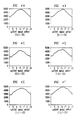
- FIG. 4A-4I are graphs of first order diffraction intensity as a function of focus variations for a latent image of 0.25 ⁇ m lines and spaces in nine different locations in a layer of energy sensitive resist material.
- FIG. 5 is a graph of first order diffraction intensity as a function of focus and dose variations for a latent image of 0.18 ⁇ m lines and spaces in 41 dose fields by 41 focus fields in a layer of energy sensitive resist material.
- FIG. 6 illustrates the relationship between the measured intensity of a series of latent images and the focus used to create those images, wherein the intensity of the latent images is measured using the process of the present invention.
- the present invention is directed to a process for controlling at least one aspect of a lithographic process by inspecting energy sensitive resist materials that have been exposed to patterned radiation.
- an energy sensitive resist material is exposed to radiation to introduce the latent image of an inspection pattern therein.
- the exposed energy-sensitive material is then inspected using a technique designed to selectively detect first order and, optionally, higher order diffraction information from a portion or portions of the energy-sensitive material with the latent image therein.
- the first order and higher order diffraction information are detected selectively because the zero order diffraction information is not detected.
- the zero order diffraction information has an angle of escape from the substrate that is significantly different than the angle of escape of the first and higher order diffraction information.
- the differences in angles of escape between zero order diffraction information and first and higher order diffraction information are significant. Because of these differences, the first and higher order diffraction information is detectable selectively. Selective detection is obtained by selecting an objective with a focal length and a numerical aperture that collects the desired diffraction information without collecting the zero order diffraction information.
- the first order diffraction information is used to either control the lithographic process or to characterize the mask (also referred to as a reticle) of the lithographic exposure tool (e.g. a deep UV lithography tool, a SCALPEL tool) used in the lithographic process.
- the lithographic parameters controlled by the present process include lamp intensity, focus, exposure dose, source coherence, and bake temperature.
- FIG. 1 A typical lithographic process is illustrated schematically in FIG. 1. Exposing radiation 10 is directed toward a layer of energy sensitive resist material 20 formed on a substrate 25. The energy sensitive resist material 20 is then patternwise exposed to radiation. One way to effect the desired patternwise exposure is to interpose a mask 30 between the source of exposing radiation 10 and the energy sensitive resist material 20. The lines 40 in the mask 30 are apertures through which the radiation passes to the energy sensitive resist material 20. Each of the lines 50 in the energy sensitive resist material is a latent feature. The radiation causes a change in the exposed energy sensitive resist material. This change is either a chemical change and/or a structural change in the resist material composition. These changes typically cause the refractive index of the material to change. The chemical difference between the exposed energy sensitive resist material and the unexposed energy sensitive resist material is exploited to develop the pattern 60 in the energy sensitive material.
- the present process is used in conjunction with lithographic processes for device fabrication.
- the materials and conditions used to introduce the latent image of a pattern in an energy sensitive material are those that are typically used in processes for device fabrication.
- One skilled in the art is capable of selecting the appropriate materials and conditions for a particular application. Since the process provides particular advantages when the design rules for the fabricated devices are 0.5 ⁇ m or less, the exposing radiation will typically be ultraviolet radiation, x-ray radiation, or electron beam radiation.
- the energy sensitive resist materials selected are those that are suitably sensitive to radiation in the ultraviolet or x-ray range, or to electron beam radiation.
- a spatially resolved image of the latent feature or features in the energy sensitive material is obtained. This is accomplished by selecting a glancing angle that is suitable for directing the first and higher order diffraction from the image into the objective and directing zero order diffraction from the image away from the objective. Based upon the wavelength of the incident radiation, the order of the diffraction, and the period of the inspection pattern, the angular escape limits of the diffraction of a particular order are determined for a particular glancing angle. The glancing angle that provides the desired order of diffraction to the objective (based on the numerical aperture and the focal length of that objective) is then selected.
- the zero order diffraction from the image is not directed into the objective.
- the image is then illuminated using a beam of radiation that impinges upon the resist at the prescribed glancing angle.
- a glancing angle is the angle at which the probe beam impinges upon the substrate relative to the substrate surface.
- the radiation reflected from the surface is then collected by an objective.
- the objective is coupled to a video camera or like device, which is used to capture data which is then used to ascertain and evaluate the latent image in the energy sensitive resist material.
- a helium cadmium illumination probe ( ⁇ of about 320 nm to about 440 nm) is suitable. Consequently, the process of the present invention is sufficiently robust so that those patterns having a wide range of periods are inspected using a single apparatus.
- the glancing angle and the numerical aperture are selected so that only first order and higher diffraction is collected by the objective.
- first order and higher diffraction is not a reflection or a refraction intensity.
- Diffraction patterns or an intensity distribution due to a sinusoidal phase grating is defined by the following relationship: As defined by the above equation, the displacement or angular dispersion of the qth order from the zero order is qf 0 ⁇ z.
- first order and higher order diffraction patterns are present in radiation that is reflected from periodic structures such as gratings.
- zero order diffraction is not collected by the objective. This is in contrast to the techniques in which the latent image is inspected using radiation that impinges on the energy sensitive resist material at an angle that is normal to the surface of the resist material.
- first order and higher diffraction that is collectable when the radiation impinges normal to the surface is limited by the period of features (i.e. a series of lines and spaces refers to gratings).
- the maximum first order diffraction is reflected from the surface 100 of the energy sensitive material 110 at an angle ⁇ (111) from the probe beam 120 which is normal to the surface.
- ⁇ ⁇ m/d
- ⁇ the wavelength of the incident radiation
- m the order of dispersion
- d the period of the grating under inspection
- the angle of dispersion gets larger as the period gets smaller. Therefore, as the period gets smaller, the numerical aperture required to capture the first order and higher diffraction gets larger.
- the minimum grating period for which latent grating dispersion intensity information is resolvable is about 350 nm.
- the wavelength of the incident radiation is selected to be outside the range of wavelengths that induce a chemical change in the energy sensitive resist material. For example, if the energy sensitive material is sensitive to radiation in the wavelength range of about 190 nm to about 350 nm, then the selected incident radiation is outside this wavelength range.
- the glancing angle is in the range of about 5 degrees to about 60 degrees from the surface of the substrate when the source of the incident radiation is a HeNe laser (wavelength of 632.8 nm).
- the sine of the glancing angle is the wavelength divided by the period of the structure being inspected.
- the period of the features is 300 nm, which corresponds to 0.15 ⁇ m lines and spaces at the HeNe wavelength.
- the period of the features is 782.2 nm which, corresponds to 0.391 ⁇ m lines and spaces at the HeNe wavelength. It is in this manner that the glancing angle prescribes the maximum and minimum feature size that can be inspected for a particular wavelength of incident radiation using the process of the present invention.
- a glancing angle of about 12°, an NA of about 0.85 and a HeNe laser are used to inspect 0.2 ⁇ m lines and spaces. If the source of the incident radiation is changed to a HeCd UV source, then 0.1 ⁇ m lines and spaces can be inspected using the same glancing angle and NA. In another embodiment, a glancing angle of about 20° is used to inspect 0.25 ⁇ m lines and spaces.
- a beam of radiation 200 is incident on the surface 210 of an energy sensitive resist material 220.
- the energy sensitive resist material 220 has the latent image 230 of a pattern of lines and spaces therein.
- the numerical aperture of the objective is illustrated schematically as ring 240.
- the dashed line 250 illustrates the maximum dispersion angle for collection by the objective.
- the wavelength of the incident radiation In order to decrease the dispersion angle without changing the glancing angle or the NA, the wavelength of the incident radiation must be reduced.
- the glancing angle 260 In order for the first order diffraction information 250 to be directed into the objective 240, the glancing angle 260 must be within a certain range. As previously noted the prescribed range will depend upon the wavelength of the probe beam and the numerical aperture and focal length of the objective receiving the first order diffraction information. As is apparent from FIG. 3, the first order diffraction information is directed into the numerical aperture 240 of the objective. The information is then conveyed to a device such as a video camera in order to
- the particular wavelength of the incident radiation is selected based upon the sensitivity of the energy sensitive resist material containing the latent image and the numerical aperture of the objective.
- the wavelength of the incident radiation must no destroy or alter the latent image under inspection. Therefore the wavelength of the incident radiation is selected so that incident radiation will not induce a change in the energy sensitive material that will either destroy or alter the latent image therein.
- the wavelength is also selected to ensure that the first order diffraction intensity is collected by the objective. Since the glancing angle is a function of the wavelength of the incident radiation, if the wavelength is too large, then the glancing angle is also too large. For example, if the energy sensitive material is sensitive to deep ultraviolet radiation (i.e. about 190 nm to about 300 nm) then laser illumination sources such as HeNe and HeCd (which provide incident radiation in the wavelength range of 632.8 nm to about 325 nm) are contemplated as suitable.
- a semiconductor wafer was coated with a layer of an energy sensitive material.
- an ARCH II photoresist obtained from the Olin Microelectronics Group of East Buffalo, Rhode Island
- the thickness of the resulting films was about 630 nm.
- the photoresist films were patternwise exposed to patterned radiation with a wavelength of 248 nm.
- the exposure tool was a GCS XLS deep-ultraviolet excimer laser-based stepper, which was obtained from GCA.
- the radiation was patterned by transmission through a mask having a pattern of 0.25 ⁇ m lines and spaces (0.5 ⁇ m period).
- the mask had multiple arrays of line and space patterns, one in which the lines and spaces were in the horizontal direction and one in which the lines and spaces were in the vertical direction, in the exposure field.
- the mask was used to introduce a number of latent images into a layer of energy sensitive resist material formed on a silicon wafer. After a latent image was introduced, the wafer was stepped to the next position and a subsequent latent image was introduced. The stepper micro-stepped the wafer in a serpentine fashion, thereby introducing a series of latent images in that serpentine pattern in the energy sensitive material..
- a variable of the exposure apparatus or tool e.g. focus, dose, etc.
- the array contains X-Y grating locations as diffraction intensities (Z) at each location. The location at which the image exhibits maximum intensity is the point at which the best focus was obtained.
- the apparatus used to inspect the latent image was a microscope fitted with a micropositioning X-Y stage with controller.
- the latent images were inspected by placing the wafer on which they were formed onto the micropositioning stage.
- Computer control of the micropositioning stage moves the wafer within the capturing range of the microscope objective.
- the objective used to obtain the first order diffraction information reflected from the wafer had a 0.85 NA and a 12 mm long focal distance.
- the objective was optically coupled to a video camera.
- a helium neon laser beam with a wavelength of 632 nm and mounted on the microscope was split into two beams using a beam splitter. Both beams were directed onto the surface of the wafer at a 20° glancing angle. One beam was oriented to illuminate the vertical gratings and the other beam was rotated 90° from the first to illuminate the horizontal gratings.
- An infrared laser auto focusing system was used to keep the image in focus and correct for changes in the distance between the objective and the wafer plane.
- the objective was placed physically in front of a photomultiplier tube.
- the probe beam was directed onto the latent images in the layer of energy sensitive material on the wafer surface.
- Angular dispersion intensity was created by the latent image.
- the objective and the photomultiplier tube were in the optical path of the higher order diffraction (i.e. first and above) from the grating. The objective therefore was used to allow only the intensities of the higher order diffractions to collect in the photomultiplier tube.
- the information collected by the photomultiplier tube was converted from analog to digital representation.
- the first order diffraction information obtained in the above-described manner was used to adjust the focus of the stepper.
- a mask with both horizontal and vertical grating patterns was used to pattern radiation. Multiple latent images of these patterns were introduced into the energy sensitive material. The stepper focus and the position of the energy sensitive material were adjusted for each image.
- First order diffraction information for each latent image was obtained by directing the HeNe laser beam at the latent image in the previously described manner. This information provided a relationship between the focus and the intensity of the light reflected from the surface of the wafer.
- FIGs. 4A-4I Each graph represents a map of the intensity of the series of 25 exposures. The optimum focus in each of FIGs. 4A-4I is indicated by the maximum intensity. By observing the maximum intensity in each of FIGs. 4A-4I, an average optimum focus was readily determined.
- a SCALPEL mask was used to introduce an image of the series of 180 nm lines and spaces in an energy sensitive material.
- An ARCH I Photoresist obtained from the Olin Microelectronics Group of East Buffalo, Rhode Island
- the exposure field size was 250 ⁇ m by 250 ⁇ m.
- the focus In the subsequent exposure in the x-direction, the focus remained fixed and the dose was changed from exposure to exposure (i.e. 7 ⁇ C/cm 2 to 15 ⁇ C/cm 2 in 0.2 ⁇ C/cm 2 increments). The focus remained fixed for all seventy exposures in a given row.
- the stepper then positioned the wafer back at its origin.
- the stepper then moved the wafer along the y-axis of the stepper's range of motion.
- a second row of latent images was then created.
- each latent image was created using a fixed, second focus.
- the dose was varied from exposure to exposure in the second row in the same manner that it was varied from exposure to exposure in the first row.
- the process was repeated to create twenty rows of latent images. Each row had seventy exposures.
- the latent images in a given row were generated using a fixed focus, but the focus was varied (i.e. a focus varied from 0 to 400 ⁇ m in ????? ⁇ m increments) from row to row. Consequently, 1400 exposure fields were generated, wherein each field had a unique dose and focus.
- a three-dimensional dose/focus matrix was created, where the z-axis was the sensitivity or diffraction intensity for a particular value of dose and focus.
- the three-dimensional dose/focus matrix is illustrated in FIG. 5.
- the apparatus used to inspect the latent image for diffraction intensity was the same as the apparatus described in Example 1.
- the maximum Z value illustrated as 300 in FIG. 5 corresponds to the best combination of focus and dose.
- FIG. 6 illustrates the relationship between the focus of each latent image and the image intensity for both the "horizontal" and “vertical” features.
- the image intensity as a function of focus for the vertical features is illustrated as line 310.
- the image intensity as a function of focus for the horizontal features is illustrated as 320.
- the best focus is indicated by the point on the curves 310 and 320 that corresponds to the peak intensity.
Landscapes
- Physics & Mathematics (AREA)
- General Physics & Mathematics (AREA)
- Exposure And Positioning Against Photoresist Photosensitive Materials (AREA)
- Exposure Of Semiconductors, Excluding Electron Or Ion Beam Exposure (AREA)
- Photosensitive Polymer And Photoresist Processing (AREA)
Applications Claiming Priority (2)
| Application Number | Priority Date | Filing Date | Title |
|---|---|---|---|
| US15162898A | 1998-09-11 | 1998-09-11 | |
| US151628 | 1998-09-11 |
Publications (1)
| Publication Number | Publication Date |
|---|---|
| EP0985977A1 true EP0985977A1 (de) | 2000-03-15 |
Family
ID=22539573
Family Applications (1)
| Application Number | Title | Priority Date | Filing Date |
|---|---|---|---|
| EP99306919A Withdrawn EP0985977A1 (de) | 1998-09-11 | 1999-08-31 | Analyse von latenten Bildern bei der Herstellung von integrierten Schaltkreisen |
Country Status (3)
| Country | Link |
|---|---|
| EP (1) | EP0985977A1 (de) |
| JP (1) | JP2000091230A (de) |
| KR (1) | KR20000047481A (de) |
Cited By (6)
| Publication number | Priority date | Publication date | Assignee | Title |
|---|---|---|---|---|
| DE10121178B4 (de) * | 2001-04-30 | 2005-12-01 | Infineon Technologies Ag | Experimentelles Verfahren zur Verifikation von Abbildungsfehlern bei Fotomasken |
| DE10121179B4 (de) * | 2001-04-30 | 2005-12-22 | Infineon Technologies Ag | Experimentelles Verfahren zur Verifikation von Abbildungsfehlern bei optischen Belichtungsgeräten |
| SG125926A1 (en) * | 2002-11-01 | 2006-10-30 | Asml Netherlands Bv | Inspection method and device manufacturing method |
| SG138445A1 (en) * | 2003-02-14 | 2008-01-28 | Asml Netherlands Bv | Device and method for wafer alignment with reduced tilt sensitivity |
| US8184264B2 (en) | 2008-12-01 | 2012-05-22 | Micron Technologies, Inc. | Calibration methods and devices useful in semiconductor photolithography |
| WO2025082683A1 (en) * | 2023-10-17 | 2025-04-24 | Asml Netherlands B.V. | Laser diffraction optical microscopy for ultra-thin pattern wafer |
Families Citing this family (2)
| Publication number | Priority date | Publication date | Assignee | Title |
|---|---|---|---|---|
| JP5434352B2 (ja) * | 2009-08-06 | 2014-03-05 | 株式会社ニコン | 表面検査装置および表面検査方法 |
| JP5434353B2 (ja) * | 2009-08-06 | 2014-03-05 | 株式会社ニコン | 表面検査装置および表面検査方法 |
Citations (3)
| Publication number | Priority date | Publication date | Assignee | Title |
|---|---|---|---|---|
| EP0469765A1 (de) * | 1990-07-31 | 1992-02-05 | AT&T Corp. | Überwachungsmethode von latenten Photolack-Bildern |
| US5556726A (en) * | 1994-05-12 | 1996-09-17 | International Business Machines Corporation | Photolithographic dose determination by diffraction of latent image grating |
| US5673101A (en) * | 1994-06-02 | 1997-09-30 | U.S. Philips Corporation | Method of repetitively imaging a mask pattern on a substrate, and apparatus for performing the method |
-
1999
- 1999-08-31 EP EP99306919A patent/EP0985977A1/de not_active Withdrawn
- 1999-09-09 JP JP11255687A patent/JP2000091230A/ja active Pending
- 1999-09-10 KR KR1019990038548A patent/KR20000047481A/ko not_active Withdrawn
Patent Citations (3)
| Publication number | Priority date | Publication date | Assignee | Title |
|---|---|---|---|---|
| EP0469765A1 (de) * | 1990-07-31 | 1992-02-05 | AT&T Corp. | Überwachungsmethode von latenten Photolack-Bildern |
| US5556726A (en) * | 1994-05-12 | 1996-09-17 | International Business Machines Corporation | Photolithographic dose determination by diffraction of latent image grating |
| US5673101A (en) * | 1994-06-02 | 1997-09-30 | U.S. Philips Corporation | Method of repetitively imaging a mask pattern on a substrate, and apparatus for performing the method |
Non-Patent Citations (3)
| Title |
|---|
| HICKMAN K C ET AL: "USE OF DIFFRACTED LIGHT FROM LATENT IMAGES TO IMPROVE LITHOGRAPHY CONTROL", JOURNAL OF VACUUM SCIENCE AND TECHNOLOGY: PART B, vol. 10, no. 5, 1 September 1992 (1992-09-01), pages 2259 - 2266, XP000322772, ISSN: 0734-211X * |
| SHOAIB ZAIDI ET AL: "METROLOGY SENSORS FOR ADVANCED RESISTS", PROCEEDINGS OF THE SPIE, vol. 2196, 28 February 1994 (1994-02-28), pages 341 - 351, XP000562171 * |
| STURTEVANT J L ET AL: "POST-EXPOSURE BAKE AS A PROCESS-CONTROL PARAMETER FOR CHEMICALLY- PHOTORESIST", PROCEEDINGS OF THE SPIE, vol. 1926, 2 March 1993 (1993-03-02), pages 106 - 114, XP000646475 * |
Cited By (8)
| Publication number | Priority date | Publication date | Assignee | Title |
|---|---|---|---|---|
| DE10121178B4 (de) * | 2001-04-30 | 2005-12-01 | Infineon Technologies Ag | Experimentelles Verfahren zur Verifikation von Abbildungsfehlern bei Fotomasken |
| DE10121179B4 (de) * | 2001-04-30 | 2005-12-22 | Infineon Technologies Ag | Experimentelles Verfahren zur Verifikation von Abbildungsfehlern bei optischen Belichtungsgeräten |
| SG125926A1 (en) * | 2002-11-01 | 2006-10-30 | Asml Netherlands Bv | Inspection method and device manufacturing method |
| US7151594B2 (en) | 2002-11-01 | 2006-12-19 | Asml Netherlands B.V. | Test pattern, inspection method, and device manufacturing method |
| US7312860B2 (en) | 2002-11-01 | 2007-12-25 | Asml Netherlands B.V. | Test pattern, inspection method, and device manufacturing method |
| SG138445A1 (en) * | 2003-02-14 | 2008-01-28 | Asml Netherlands Bv | Device and method for wafer alignment with reduced tilt sensitivity |
| US8184264B2 (en) | 2008-12-01 | 2012-05-22 | Micron Technologies, Inc. | Calibration methods and devices useful in semiconductor photolithography |
| WO2025082683A1 (en) * | 2023-10-17 | 2025-04-24 | Asml Netherlands B.V. | Laser diffraction optical microscopy for ultra-thin pattern wafer |
Also Published As
| Publication number | Publication date |
|---|---|
| JP2000091230A (ja) | 2000-03-31 |
| KR20000047481A (ko) | 2000-07-25 |
Similar Documents
| Publication | Publication Date | Title |
|---|---|---|
| US6429930B1 (en) | Determination of center of focus by diffraction signature analysis | |
| JP4787232B2 (ja) | 測定方法、検査装置、およびリソグラフィ装置 | |
| US6466315B1 (en) | Method and system for reticle inspection by photolithography simulation | |
| JP3972035B2 (ja) | 検査方法とデバイス製造方法 | |
| KR100923543B1 (ko) | 각도-분해 분광 리소그래피 특성화를 위한 방법 및 장치 | |
| EP3394677B1 (de) | Verfahren und strukturierungsvorrichtungen sowie vorrichtungen zur messung der fokusleistung einer lithografievorrichtung, verfahren zur herstellung der vorrichtung | |
| TWI435182B (zh) | 角度分辨散射計及檢查方法 | |
| EP0729072B1 (de) | Verfahren zur Herstellung einer Vorrichtung, wobei eine Nahfeldabbildung von latenten in energieempfindlichen Lackmaterialen erzeugten merkmalen zur Steuerung des Verfahrens verwendet wird | |
| JP3981664B2 (ja) | 検査方法およびデバイス製造方法 | |
| JP2008177567A (ja) | 測定方法、検査装置およびリソグラフィ装置 | |
| JP2008083032A (ja) | 検査方法および装置、リソグラフィ装置、リソグラフィ処理セルおよびデバイス製造方法 | |
| TWI796535B (zh) | 測量圖案化製程之參數的方法、度量衡裝置與目標 | |
| KR20050035153A (ko) | 단면 분석법에 의한 초점 중심의 결정 | |
| KR102668160B1 (ko) | 리소그래피 장치의 포커스 성능을 측정하는 장치들 및 패터닝 디바이스들 및 방법들, 디바이스 제조 방법 | |
| JP2003022968A (ja) | リソグラフィ装置の較正方法、リソグラフィ装置の較正に使用するマスク、リソグラフィ装置、デバイス製造方法、該デバイス製造方法により製造されたデバイス | |
| US5830611A (en) | Use of diffracted light from latent images in photoresist for optimizing image contrast | |
| KR20000047481A (ko) | 디바이스 제조용 리소그래피 공정 | |
| Milner et al. | Latent image exposure monitor using scatterometry | |
| US7016030B2 (en) | Extended surface parallel coating inspection method | |
| US20060215140A1 (en) | Method of measuring the performance of an illumination system | |
| JP3900601B2 (ja) | 露光条件選択方法、及び該方法で使用される検査装置 | |
| TW202248884A (zh) | 用於判定與微影製程相關之隨機度量之方法 | |
| NL2022031A (en) | Methods and patterning devices and apparatuses for measuring focus performance of a lithographic apparatus, device manufacturing method | |
| TW201118366A (en) | Scatterometer method and apparatus, lithographic apparatus, lithographic processing cell and device manufacturing method |
Legal Events
| Date | Code | Title | Description |
|---|---|---|---|
| PUAI | Public reference made under article 153(3) epc to a published international application that has entered the european phase |
Free format text: ORIGINAL CODE: 0009012 |
|
| 17P | Request for examination filed |
Effective date: 19990910 |
|
| AK | Designated contracting states |
Kind code of ref document: A1 Designated state(s): DE FR GB |
|
| AX | Request for extension of the european patent |
Free format text: AL;LT;LV;MK;RO;SI |
|
| AKX | Designation fees paid |
Free format text: DE FR GB |
|
| 17Q | First examination report despatched |
Effective date: 20020212 |
|
| STAA | Information on the status of an ep patent application or granted ep patent |
Free format text: STATUS: THE APPLICATION IS DEEMED TO BE WITHDRAWN |
|
| 18D | Application deemed to be withdrawn |
Effective date: 20020625 |