EP0986084A2 - Elektronenemissionsvorrichtung und Bilderzeugungsgeräts dieselbe beinhaltend - Google Patents
Elektronenemissionsvorrichtung und Bilderzeugungsgeräts dieselbe beinhaltend Download PDFInfo
- Publication number
- EP0986084A2 EP0986084A2 EP99117482A EP99117482A EP0986084A2 EP 0986084 A2 EP0986084 A2 EP 0986084A2 EP 99117482 A EP99117482 A EP 99117482A EP 99117482 A EP99117482 A EP 99117482A EP 0986084 A2 EP0986084 A2 EP 0986084A2
- Authority
- EP
- European Patent Office
- Prior art keywords
- thin
- electron emission
- electron
- insulator layer
- metal electrode
- Prior art date
- Legal status (The legal status is an assumption and is not a legal conclusion. Google has not performed a legal analysis and makes no representation as to the accuracy of the status listed.)
- Withdrawn
Links
Images


Classifications
-
- B—PERFORMING OPERATIONS; TRANSPORTING
- B82—NANOTECHNOLOGY
- B82Y—SPECIFIC USES OR APPLICATIONS OF NANOSTRUCTURES; MEASUREMENT OR ANALYSIS OF NANOSTRUCTURES; MANUFACTURE OR TREATMENT OF NANOSTRUCTURES
- B82Y10/00—Nanotechnology for information processing, storage or transmission, e.g. quantum computing or single electron logic
-
- H—ELECTRICITY
- H01—ELECTRIC ELEMENTS
- H01J—ELECTRIC DISCHARGE TUBES OR DISCHARGE LAMPS
- H01J1/00—Details of electrodes, of magnetic control means, of screens, or of the mounting or spacing thereof, common to two or more basic types of discharge tubes or lamps
- H01J1/02—Main electrodes
- H01J1/30—Cold cathodes, e.g. field-emissive cathode
- H01J1/312—Cold cathodes, e.g. field-emissive cathode having an electric field perpendicular to the surface, e.g. tunnel-effect cathodes of metal-insulator-metal [MIM] type
-
- H—ELECTRICITY
- H01—ELECTRIC ELEMENTS
- H01J—ELECTRIC DISCHARGE TUBES OR DISCHARGE LAMPS
- H01J31/00—Cathode ray tubes; Electron beam tubes
- H01J31/08—Cathode ray tubes; Electron beam tubes having a screen on or from which an image or pattern is formed, picked up, converted, or stored
- H01J31/10—Image or pattern display tubes, i.e. having electrical input and optical output; Flying-spot tubes for scanning purposes
- H01J31/12—Image or pattern display tubes, i.e. having electrical input and optical output; Flying-spot tubes for scanning purposes with luminescent screen
- H01J31/123—Flat display tubes
- H01J31/125—Flat display tubes provided with control means permitting the electron beam to reach selected parts of the screen, e.g. digital selection
- H01J31/127—Flat display tubes provided with control means permitting the electron beam to reach selected parts of the screen, e.g. digital selection using large area or array sources, i.e. essentially a source for each pixel group
-
- H—ELECTRICITY
- H01—ELECTRIC ELEMENTS
- H01J—ELECTRIC DISCHARGE TUBES OR DISCHARGE LAMPS
- H01J9/00—Apparatus or processes specially adapted for the manufacture, installation, removal, maintenance of electric discharge tubes, discharge lamps, or parts thereof; Recovery of material from discharge tubes or lamps
- H01J9/02—Manufacture of electrodes or electrode systems
- H01J9/022—Manufacture of electrodes or electrode systems of cold cathodes
Definitions
- the present invention relates generally to an electron emission device, and more particularly to an electron emission display device which has a plurality of electron emission devices arranged in an image display array, for example, in a matrix form.
- a Field Emission Display is known as a planar emission display device equipped with an array of cold cathode electron emission sources which does not require cathode heating.
- the emission principle of, for example, an FED using Spindt-type cold cathodes of minute protrusions is as follows. Its emission principle is like a Cathode Ray Tube (CRT), although this FED has a cathode array of Spindt-type protrusions which is different from that of CRT.
- CTR Cathode Ray Tube
- This FED has a problem of low production yield because the manufacture of the minute Spindt-type emitter arrays as a cold cathode is complex and involves many processes.
- the electron emission device with the MIM structure comprises an Al underlayer as a base electrode, an Al 2 O 3 insulator layer with about 10 nm thickness, and a Au overlayer, as a top electrode with about 10 nm thickness which are formed in order on the substrate.
- MIM metal-insulator-metal
- the electron emission device with the MIM structure does not yet provide a sufficient amount of emitted electrons.
- an electron emission device with the MIM structure which is manufactured by this anodization method ensures an emission current of about 1 x 10 -5 A/cm 2 and an electron emission efficiency of about 0.1 %.
- the MIM type electron emission device whose insulator layer has a thickness of several tens of nanometers to several micrometers does not have a plane forming status formed uniformly resulting in a problem of bringing an unstable electron emission property of the device.
- a surface conductive type electron emission device is further known.
- This type device is manufactured as follows. First a pair of facing electrodes are formed on a substrate of an insulative material. Subsequently a conductive thin film is bridged between the facing electrodes.
- the conductive thin film bridge is electrified as an electrifying process so as to form a gap or break as an electron emission portion therein. Since such a gap or break is generated by locally destroying, denaturing or modifying the conductive thin film, there are problems in that the structural homogeneity in the electron emission portion is inferior and, the re-productivity in shape of the electron emission portion is very poor.
- the electron emission portion is restricted in shape within a linear line.
- the present invention has been made in view of the above circumstances, and thus an object thereof is to provide an electron emission device having an electron emitting efficiency high enough to stably emit electrons at a low voltage applied thereto, and moreover a display apparatus including a flat panel display device which employs a plurality of such electron emission devices.
- an electron emission device which comprises:
- said island-like regions are electron emission sites.
- said insulator layer is made of dielectric and has a film thickness of 50 nm or greater.
- the thin-film metal electrode is terminated on the insulator layer in each of the island-like regions.
- the insulator layer is terminated on the electron-supply layer in each of the island-like regions.
- each of the island-like regions is a recess formed in a flat surface of the thin-film metal electrode.
- the insulator layer and the thin-film metal are formed by a physical vapor deposition and/or chemical vapor deposition.
- a minute particle is provided in each of the island-like regions.
- an inverse tapered block is provided in each of the island-like regions.
- a method of manufacturing an electron emission device having a plurality of island-like regions where thicknesses of an insulator layer and a thin-film metal electrode gradually decrease comprises the steps of:
- the method further comprises a step of applying a voltage across the electron-supply layer and the thin-film metal electrode for growth of conductive paths after the thin-metal electrode forming step.
- the method further comprises a step of removing the minute particles from the island-like regions after the thin-metal electrode forming step.
- the method further comprises a step of applying a voltage across the electron-supply layer and the thin-film metal electrode for growth of conductive paths after the minute particle removing step.
- a method of manufacturing an electron emission device having a plurality of island-like regions where thicknesses of an insulator layer and a thin-film metal electrode gradually decrease comprises the steps of:
- the method further comprises a step of applying a voltage across the electron-supply layer and the thin-film metal electrode for growth of conductive paths after the thin-metal electrode forming step.
- the method further comprises a lift-off step of removing the inverse tapered blocks from the island-like regions after the thin-metal electrode forming step.
- the method further comprises a step of applying a voltage across the electron-supply layer and the thin-film metal electrode for growth of conductive paths after the lift-off step.
- said block forming step includes steps of forming an inverse tapered block material layer on said substrate, forming a resist mask on said inverse tapered block material layer by photolithography for exposing part of at least said electron-supply layer, and carving said inverse tapered blocks having said overhang portions by dry etching or wet etching.
- the present invention still further provides an electron emission display device which comprises:
- said insulator layer is made of dielectric and has a film thickness of 50 nm or greater.
- the thin-film metal electrode is terminated on the insulator layer in each of the island-like regions.
- the insulator layer is terminated on the electron-supply layer in each of the island-like regions.
- each of the island-like regions is a recess formed in a flat surface of the thin-film metal electrode.
- the insulator layer and the thin-film metal are formed by a physical vapor deposition and/or chemical vapor deposition.
- the display device further comprises plural insulative support members formed on said first substrate and disposed between adjacent ones of said electron emission devices so as to enclose the electron emission devices for partitioning them, wherein the distance from said first substrate to the surfaces of said insulative support members proximate to said vacuum space is substantially equal to the distance from said first substrate to the surface of said thin-film metal electrodes proximate to said vacuum space.
- the display device further comprises a plurality of bus electrodes, each of which is arranged in a stripe form to electrically connect adjacent ones of said thin-film metal electrodes, wherein said ohmic electrodes and said electrodes are stripe-like electrodes and arranged to extend perpendicular to each other.
- said first substrate includes a plurality of first insulative ramparts, each of which disposed between said electron emission devices and protruding into said vacuum space, whereas said second substrate includes a plurality of second ramparts each of which protrudes into said vacuum space to abut to said first ramparts.
- the thicknesses of island-like portions of the insulator layer and the thin-film metal electrode gradually decrease in a direction along which their interface extends, the amount of electrons increases that are emitted from the island-like regions.
- the electron emission device of the invention is a planar or spot-like electron emission diode and can be adapted to high speed devices such as a source of a pixel vacuum tube or bulb, an electron emission source of a scanning or transmission electron microscope, a vacuum-micro electronics device and the like.
- this electron emission device can serve as a minute microwave tube or a diode which emits electromagnetic waves with millimeter or sub-millimeter wavelength, and also can serve as a high speed switching device.
- an ohmic electrode 11 made of aluminum (Al), tungsten (W), titanium nitride (TiN), copper (Cu), chromium (Cr) or the like on a first substrate 10 made of a glass or the like
- the insulator layer 13 is deposited in considerably thicker thicknesses so as to have a thickness of 50 nm or greater.
- These layer are formed through the sputtering method by using a gas of Ar, Kr or Xe or a mixture thereof, or a gas mixture essentially consisting of one of those rare gases with O 2 , N 2 or the like mixed therein, under the sputtering conditions of a gas pressure of 0.1 to 100 mTorr, preferably 0.1 to 20 mTorr and the forming rate of 0.1 to 1000 nm/min, preferably 0.5 to 100 nm/min.
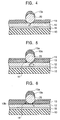
- each island-like region 14 is formed as a recess on the flat surface of the thin-film metal electrode 15.
- the thin-film metal electrode 15 ends at an edge "A" on the insulator layer 13.
- the insulator layer 13 in each island-like region 14 ends at an edge "B" on the electron-supply layer 12.
- the plural island-like regions 14 as recesses are formed in the following manner.
- the electron-supply layer 12 is formed by sputtering on the substrate 10 on which the ohmic electrode 11 is formed, as shown in Figure 2.
- a plurality of spherical minute particles 20 are sprayed on the electron-supply layer 12 as shown in Figure 3 but showing only one minute particle.
- the minute particles need not be spherical to ensure electron emission.
- spherical particles with an isotropic shape such as spacers used for a liquid crystal display panel, ball mills or the like are desirable in consideration of the uniformity of the grain boundary portions of the minute particles, uniform dispersion on a film and no flocculation. A variation in the distribution of particle sizes should be small.
- the available materials for the minute particles are an insulator, semiconductor and metal. When metal minute particles are to be used in which case the device may be short-circuited, the minute particles should be removed after the thin-film metal electrode 15 is formed.
- an insulator 13, 13a is deposited on the electron-supply layer 12 and the minute particles 20, thus forming the insulator layer 13 which is a thin film of the insulator.
- the insulator gas comes around the portion where the electron-supply layer 12 contacts each minute particle 20, thus forming an insulator layer portion whose thickness gradually decreases from the predetermined thickness of the insulator layer 13.
- This insulator layer portion ends at the edge "B" on the electron-supply layer 12 in each island-like region 14.
- metal layers 15, 15a are deposited on the insulator layer 13 and the minute particles 20, thus forming the thin-film metal electrode 15, as shown in Figure 5.
- the metal gas comes around the portion where the electron-supply layer 12 contacts each minute particle 20 from a clearance between the insulator layer 13 and that minute particle 20, thus forming a thin-film metal electrode portion whose thickness gradually decreases from the predetermined thickness of the thin-film metal electrode 15.
- This thin-film metal electrode portion ends at the edge "A" on the insulator layer 13 in each island-like region 14.
- each minute particle 20 and the insulator layer 13 or the thin-film metal electrode 15 and the insulator layer 13 and the thin-film metal electrode 15 continuously and gradually become thinner toward the contact point between that minute particle and the electron-supply layer 12 from that boundary.
- the island-like regions 14 as recesses are formed around the contact surfaces under the minute particles 20 in the insulator layer 13 and the thin-film metal electrode 15.
- the dent recessed island-like regions 14 shown in Figure 1 are formed by removing the minute particles by implementing an ultrasonic cleaning or the like.
- the electron emission device may have the minute particles un-removed.
- the diameter of the minute particles is set to such a size that part of each minute particle comes out of the surface of the thin-film metal electrode on the electron emission side, i.e., each minute particle is not completely buried.
- the emission current gets lower.
- a conductive path growth step may be performed for the substrate 10 carrying electron emission devices each having the island-like region 14 the thin-film metal electrode 15 terminated on the portion of the insulator layer 13 whose thickness gradually decrease, regardless of whether or not the minute particles has been on the device.
- a pertinent voltage is applied across the electron-supply layer 12 and the thin-film metal electrode 15 to flow a given current therebetween in the conductive path growth step.
- the insulator portion between the edge "B" of the insulator layer 13 and the edge "A" of the thin-film metal electrode 15 have a high resistivity, this portion become a current path for an electron emission site. Therefore the electric current first flows at this insulator portion of the electron emission site. Thus Joule's heat occurs, so that the growth of the conductive paths is facilitated in the surface or inside of the insulator portion within the electron emission site.
- the Si portion of the electron-supply layer 12 just on and beneath the electron emission site of the insulator portion obtains a low electric resistance locally and selectively reduced, although the Si material has exhibited a high resistivity at the beginning, resulting in the increase of quantity of current.
- the conductive paths grow concentratedly and uniformly within each island-like region 14.
- the conductive path growth step prevents unwanted insulator breakdown because of the high resistivity of Si at the beginning, and contributes to a stable emission current of the resultant device.
- an auxiliary insulator layer 13b may be formed by sputtering preparately before the minute-particles spraying step so that the minute particles 20 are separated from the electron-supply layer 12 through this auxiliary insulator layer 13b, as shown in Figure 6.
- the separated distance should be in a range of several tens of angstroms to several thousand angstroms. This design can prevent short-circuiting between the electron-supply layer 12 and the thin-film metal electrode 15.
- the island-like regions 14 are not limited to crater-like recesses formed by the minute particles, but may take the shape of groove-shaped recesses 14a as shown in Figure 7 or the shape of cone-like recesses 14b as shown in Figure 9.
- the shape of the island-like regions and a method of forming the island-like regions are optional.
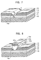
- the groove-shaped recesses 14a and the cone-like recesses 14b in examples illustrated in Figures 7 and 9 are formed in the same procedures as are used to form the island-like regions 14 above mentioned, except that the minute particles are replaced with line- or dot-shaped inverse tapered blocks 21a as shown in Figure 8 or columnar inverse tapered blocks 21b as shown in Figure 10.
- the electron emission device may have the inverse tapered blocks 21a or 21b on the electron-supply layer 12 or the auxiliary insulator layer 13b as shown in Figure 6.
- Each inverse tapered block 21a or 21b is formed of an electrically insulative material like a resist, protrudes in a direction normal to the substrate 10 and has an overhang portion 22a or 22b at its upper portion, which protrudes in a direction parallel to the substrate.
- a lift-off step is performed for removing the inverse tapered blocks 21a, 21b from the island-like regions so as to form the recessed island-like regions.
- the electron emission device has a plurality of island-like regions 14 as recesses formed uniformly on the top surface by removing the minute particles 20 or the inverse tapered blocks 21a or 21b as shown in Figure 1, 7 or 9.
- the electron emission device may have the minute particles 20 or the inverse tapered blocks 21a or 21b left in the centers of the recessed island-like regions 14 as shown in Figures 5 and 6, or Figure 8 or 10.
- a second substrate i.e., front substrate 1 made of glass and the substrate 10 are supported apart from one another in parallel by a spacer and sealed to face each other with a vacuum space 4 interposed therebetween.
- one transparent collector electrode 2 of, for example, an indium tin oxide (so-called ITO), tin oxide (SnO), zinc oxide (ZnO) or the like, is formed.
- ITO indium tin oxide
- SnO tin oxide
- ZnO zinc oxide
- the transparent collector electrodes may be arranged in groups of three in association with red (R), green (G) and blue (B) color signals in order to provide a color display panel, and voltages are applied to those three collector electrodes respectively.
- the transparent collector electrodes are separately coated with fluorescent materials 3R, G, B which are capable of emitting lights of R, G and B corresponding to the three primary colors of light respectively.
- a black stripe masks BM or back metal layer may be provided on the front substrate 1 between the fluorescent material layers 3R, G, B.
- the collector electrode 2 may be formed integrally as a monolithic film for a monochrome display panel.
- the material for the back substrate 10 is not limited to glass, and ceramics such as Al 2 O 3 , Si 3 N 4 and BN etc. may be used instead of glass.
- This electron emission device “S” can be regarded as a diode of which the thin-film metal electrode 15 at its surface is connected to a positive applied voltage Vd and the ohmic electrode 11 is connected to a ground potential as shown in Figure 1.
- Vd for example approximately 90 volt
- Id a diode current
- the insulator layer 13 has a high resistance, most of the applied electric field is applied and concentrated to the insulator layer 13.
- the electrons travel in the insulator layer 13 toward the thin-film metal electrode 15 in each island-like region 14. Some of the electrons that reach near the thin-film metal electrode 15 pass through the island-like region 14, due to the strong electric field, to be emitted out into the vacuum space.
- the electrons "e” (emission current Ie) discharged from the island-like region 14 are soon accelerated by a high voltage Vc for example approximately 5 kilovolt which is applied to an opposing collector electrode 2 (transparent electrode), and are collected with the collector electrode 2.
- Vc high voltage
- a fluorescent substance 3 is coated on the collector electrode 2, corresponding visible light is observed.
- an MIM or MIS type electron emission device whose insulator layer has a thickness of several tens of nanometers to several micrometers cannot emit electrons immediately after the simple production of the device.
- the electron emission device as produced requires a process called “forming” which applies a voltage between the thin-film metal electrode 15 and the ohmic electrode 11 in such a way that the former electrode 15 becomes positive.
- the "forming" process has not been clearly explained yet while there are various opinions about this matter, such as diffusion of an electrode material into the insulator layer, crystallization in the insulator layer, growth of the conductive path called “filament” and stoichiometric deviation in the composition of the insulator.
- the electron emission device of this embodiment there are provided a local portion of the insulator layer 13 which gradually become thinner i.e., the island-like regions 14 whose thicknesses of 13, 15 also gradually decrease, in each of which an electron emission site is formed in such a manner that the edge of the thin-film metal electrode 15 is placed on the insulator layer 13 gradually becoming thinner.
- This electron emission device is capable of emitting electrons sufficiently.
- the conductive path growth step By the conductive path growth step, the conductive minute structure existing in the surface or inside of the insulator layer within the electron emission site grows and increases.
- An effective material for the electron-supply layer 12 of the electron emission device is silicon (Si) and particularly the hydrogenated amorphous silicon (a-Si:H) in which almost of the dangling bonds of a-Si are terminated by hydrogen atoms is effective.
- silicon Si
- a-Si:H hydrogenated amorphous silicon carbide
- C carbon atoms
- a-SiN:H hydrogenated amorphous silicon nitride
- N nitrogen atoms
- silicon doped with boron, aluminium, gallium, phosphorus, indium, arsenic and/or antimony may be used for the electron-supply layer 12.
- an elemental semiconductor or a compound semiconductor of an element of a group IV, a group III-V, a group II-VI or the like such as a germanium (Ge), germanium silicon compound (Ge-Si), silicon carbide (SiC), galliumarsenide (GaAs), indium phosphide (InP), or cadmium selenide (CdSe) or CuInTe 2 can be used for the electron-supply layer 12 of the electron emission device as well.
- metals such as Al, Au, Ag and Cu are effective as the electron supplying material, Sc, Ti, V, Cr, Mn, Fe, Co, Ni, Zn, Ga, Y, Zr, Nb, Mo, Tc, Ru, Rh, Pd, Cd, Ln, Sn, Ta, W, Re, Os, Ir, Pt, Tl, Pb, La, Ce, Pr, Nd, Pm, Sm, Eu, Gd, Tb, Dy, Ho, Er, Tm, Yb, Lu and the like can be used for the electron-supply layer 12 as well.
- Silicon oxide SiO x (wherein subscribed x represents an atomic ratio) is effective as the dielectric material of and, metal oxides or metal nitrides such as LiO x , LiN x , NaO x , KO x , RbO x , CsO x , BeO x , MgO x , MgN x , CaO x , CaN x , SrO x , BaO x , ScO x , YO x , YN x , LaO x , LaN x , CeO x , PrO x , NdO x , SmO x , EuO x , GdO x , TbO x , DyO x , HoO x , ErO x , TmO x , YbO x , LuO x , TiO x , ZrO x ,
- metal complex oxides such LiAlO 2 , Li 2 SiO 3 , Li 2 TiO 3 , Na 2 Al 22 O 34 , NaFeO 2 , Na 4 SiO 4 , K 2 SiO 3 , K 2 TiO 3 , K 2 WO 4 , Rb 2 CrO 4 , Cs 2 CrO 4 , MgAl 2 O 4 , MgFe 2 O 4 , MgTiO 3 , CaTiO 3 , CaWO 4 , CaZrO 3 , SrFe 12 O 19 , SrTiO 3 , SrZrO 3 , BaAl 2 O 4 , BaFe 12 O 19 , BaTiO 3 , Y 3 Al 5 O 12 , Y 3 Fe 5 O 12 , LaFeO 3 , La 3 Fe 5 O 12 , La 2 Ti 2 O 7 , CeSnO 4 , CeTiO 4 , Sm 3 Fe 5 O 12 , EuFeO 3 , Eu 3 Fe 5
- sulfides such as FeS, Al 2 S 3 , MgS, ZnS and the like, fluorides such as LiF, MgF 2 , SmF 3 and the like, chlorides such as HgCl, FeCl 2 , CrCl 3 and the like, bromides such as AgBr, CuBr, MnBr 2 and the like, iodide such as PbI 2 , CuI, FeI 2 and the like and metal oxidized nitrides such as SiAlON and the like can be used as well for the insulator layer 13.
- fluorides such as LiF, MgF 2 , SmF 3 and the like
- chlorides such as HgCl, FeCl 2 , CrCl 3 and the like
- bromides such as AgBr, CuBr, MnBr 2 and the like
- iodide such as PbI 2 , CuI, FeI 2 and the like and metal oxidized nitrides such as Si
- C 2n Fullerene
- metal carbide such as Al 4 C 3 , B 4 C, CaC 2 , Cr 3 C 2 , Mo 2 C, MoC, NbC, SiC, TaC, TiC, VC, W 2 C, WC, ZrC and the like are also effective as the dielectric material of the insulator layer 13.
- Fullerene (C 2n ) consists of carbon atoms.
- the representative C 60 is a spherical surface basket molecule as known a soccer ball molecule. There is also known C 32 to C 960 and the like.
- the subscribed x in O x , N x and the like in the above chemical formulas represent atomic ratios and also herein after.
- the film thickness of the insulator layer 13 other than the island-like region 14 may be 50 nm or greater preferably in ranging from 100 to 1000 nm.
- Metals Pt, Au, W, Ru and Ir are effective as the material for the thin-film metal electrode 15 on the electron emission side.
- a physical vapor deposition (PVD) and/or chemical vapor deposition (CVD) is effective for the fabrication of those layers on the substrate in the method of manufacturing an electron emission device.
- the PVD method includes a vacuum deposition, MBE (Molecular Beam Epitaxy), sputtering, ion beam sputtering, ionization vacuum deposition, laser ablation and the like.
- the CVD method includes a thermal CVD, plasma CVD and MOCVD (metal-organic chemical vapor deposition). Particularly the sputtering is effective.
- Plural electron emission devices according to the invention each comprising an electron-supply layer made of Si to which B (Boron) was added were fabricated as embodiments and their characteristics were specifically examined or checked concretely.
- minute-particles sprayed substrates were as prepared in which minute particles were sprayed on the electron-supply layer of the common substrate.
- the minute particles used in this embodiment were spherical minute particles (hereinafter simply called "spacers") having a diameter of about 1.0 ⁇ m.
- the material for the minute particles was SiO 2 , and the distribution range of the particle sizes was very narrow.
- the minute particles were sprayed using the same known scheme as employed to spray spacers utilizing for a liquid crystal display device. There are two types of spraying, wet spraying and dry spraying, the former having been used for this embodiment.
- the spherical minute particles of spacers were dispersed into ethyl alcohol and were agitated sufficiently so as not to be flocculated. This particles-dispersed solution was spin-coated on the electron-supply layer, after which ethyl alcohol was removed by drying. This allowed the spherical minute particles to be uniformly coated on the electron-supply layer.
- the distribution density of the minute particles adhering onto the electron-supply layer was approximately 140 particles per mm 2 . In this way, a plurality of the minute-particles sprayed substrates were prepared as spacer substrates for the first embodiment.
- a plurality of minute-particles sprayed substrates each having an auxiliary insulator layer were prepared each of which has the same structure as the structure of the first embodiment, except that the auxiliary insulator layer of SiO 2 was formed at a 50 nm thick by sputtering immediately before the minute-particles spraying step in order to prepare a minute-particles sprayed substrate in which the minute particles were set apart from the electron-supply layer through the auxiliary insulator layer.
- plural substrates with spacers provided on the auxiliary insulator layer were prepared as SiO 2 /spacer substrates.
- a plurality of so called block substrates were prepared, each of which has an inverse tapered block formed on the electron-supply layer of the common substrate aforementioned.
- a novolac-based photoresist was used as a resist for the material of the inverse tapered block, and was coated using spin coating. After the resist was coated, a desired resist pattern was formed using a photo-mask through prebaking, exposure, postbaking and developing processes. While the pattern to be formed then can have an arbitrary shape, it should be thick enough not to be completely buried in the insulator layer that would be formed later.
- a linear, inverse tapered block of 5000 nm in thickness and 4000 nm in height, or a columnar, inverse tapered block of 2.0 ⁇ m in diameter and 4000 nm in height was formed of the resist on the electron-supply layer. While the inverse tapered block of the resist (which will sometimes be simply called “resist” hereinafter) that was used in this example had a lateral cross-section of an inverse tapered shape, it could have an arbitrary taper angle and tapering was not essential.
- a plurality of substrates with a resist block provided on the electron-supply layer were prepared as block substrates in the above manner.
- so called device substrates carrying the electron emission devices were prepared on the basis of the substrates corresponding to the first to third embodiments in such a manner that the insulator layer of SiO 2 was formed at 330 nm thick on the electron-supply layer of each of the resultant substrates, by reactive sputtering with oxygen.
- the upper portions of the spherical minute particles and the protruding portion of the inverse tapered block were exposed through the device surface, though SiO 2 was sputtered on the upper surfaces of the minute particles and the inverse tapered block.
- the insulator layer was formed on that region by the sputtered gas that came from around the contact area. Around the contact area, the insulator layer was gradually thinner toward the contact area.
- the electron emission device may be formed without performing a surface treatment on the insulator layer, or the metal electrode film may be formed after subjecting the surface of the insulator layer to sputter etching.
- the sputter etching etches or modifies the boundary portion between the minute particles and the insulator (or the resist and the insulator) so that the electrode material comes around this boundary portion more effectively when the thin film of the metal electrode is formed. This would cause electron emission more effectively.
- the sputter etching however leaves ring-like marks on the device surface that reflect the shapes of the minute particles (or ring-like or linear marks that reflect the resist pattern).
- each thin-film metal electrode was layered at the top surface after the sputter etching step.
- a plurality of device substrates for the electron emission device "S" were prepared as shown in Figure 1, so that the dispersed minute particles are removed from the minute-particles sprayed substrate of the first embodiment. Therefor each device of the fourth embodiment had only recessed island-like regions.
- the substrates of the fourth embodiment were prepared in the same steps as those of the first embodiment, except that the dispersed minute particles and the resist pattern were removed from the minute-particles sprayed substrate of the electron emission device with a resist of the first embodiment by ultrasonic cleaning using water, acetone, ethanol, methanol, isopropyl alcohol or the like.
- a plurality of device substrates for the electron emission device "S" were prepared removing inverse tapered block made of the resist from the block substrate of the third embodiment. Therefore, each device had only recesses and grooves in the island-like region.
- the substrates of the fifth embodiment were prepared in the same steps as those of the third embodiment, except that the resist pattern was removed from the block substrate of the electron emission device with a resist of the third embodiment by ultrasonic cleaning using water, acetone, ethanol, methanol, isopropyl alcohol or the like.
- a plurality of substrates of an electron emission device without recesses and grooves were prepared from the electron-supply layer substrate in the same procedures as those of the aforementioned examples, except that the dispersed minute particles and the resist pattern were not provided.
- transparent substrates were prepared by forming an ITO collector electrode and a layer of a fluorescent material in turn on the inner side of each of the transparent glass substrates 10.
- the individual electron emission devices of the first to fifth embodiments and the comparative example were assembled and produced so as to hold the device substrate and the transparent substrate apart by 5 mm in parallel by spacers in such a way that the thin-film metal electrode and the collector electrode faced each other, with the clearance vacuumed to 10 -7 Torr or 10 -5 Pa.
- the diode current Id and emission current Ie of each device were measured in the condition that the device voltage Vps of 0 to 120 V was applied between the thin-film metal electrode and the ohmic electrode of each produced device.
- the following Table shows the measured results.
- device structure in the head line denotes, from the left side, (ohmic electrode material)/(electron-supply layer material)/(island-like region)/(insulator layer material)/(thin-film metal material) which were laminated in the named order correspondingly to the embodiments above mentioned.
- Embodiment Device structure Vps (CV) Diode curt. Id(A/cm 2 ) Emission curt. Ie(A/cm 2 ) Eff.
- the spacer denotes spherical particles made of an insulator
- the resist denotes inverse tapered blocks made of a novolac based photoresist.
- the electron emission devices having recessed island-like regions of the embodiments exhibit the emission currents.
- the device with the lamination of TiN/Si+B/spacer/SiO 2 /(Pt or Au) according to the first embodiment had the emission current significantly increased from that of the comparative example.
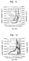
- Figures 11 and 12 show changes in the diode current Id and the emission current Ie of the electron emission device of the first embodiment in which the Pt electrode was formed and that of the comparative example when the device voltage Vps of 0 to 90 V was applied. It is apparent from those figures that the electron emission device having the recessed island-like regions has the emission current Ie increased significantly, higher by two digits than that of the comparative example.
- the maximum emission current of the first embodiment was 6.9 x 10 - 3 A/cm 2 in contrast to 1.2 x 10 -5 A/cm 2 of the comparative example.
- the average electron emission from one recessed island-like region is calculated to be 5.0 x 10 -7 A. It is also clear that the electron emission device that has recessed island-like regions provides a stable emission current Ie and diode current Id which have very slight variations, as compared with those of the comparative example.
- devices with insulator layers whose general thicknesses were 50 nm or thicker but whose thicknesses varied within a range of 50 nm to 1000 nm, were prepared under the above conditions of the first embodiment, and the variable electron emission efficiency, ⁇ Ie/(Ie+Id) x 100 ⁇ (%) , with respect to those thicknesses of the insulator layers was measured as a voltage of 200 V or lower was applied to the devices. The results showed that the devices having the insulator layers with those specified thicknesses demonstrated the electron emission efficiency of 0.1% or greater.
- the electron emission device whose electron-supply layer contains Si alone and no B added also demonstrated the same effects as those examples.
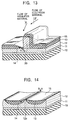
- each island-like region 14 where the thicknesses of the insulator layer 13 and the thin-film metal electrode 15 gradually decrease toward a shielding partition 20a may be formed on one side wall of the associated groove or recess, as shown in Figure 13.
- the grooved or recessed island-like regions 14 shown in Figure 13 can be formed as follows. First, like the linear, tapered block 21a shown in Figure 8, the shielding partition 20a is formed of a resist on the substrate 10 on which the ohmic electrode 11 and the electron-supply layer 12 are formed in order. Then, the insulator layer 13 is formed by sputtering or the like.
- the surface of the electron-supply layer 12 on the substrate 10 is inclined with respect to the direction of the flow of the sputtered insulator material, so that the insulator layer 13 will have a portion where a smaller amount of the insulator material is deposited on one side of the shielding partition 20a or where the thickness of the insulator layer gradually decreases toward the shielding partition 20a.
- the surface of the insulator layer 13 on the substrate 10 is inclined with respect to the direction of the flow of the sputtered material for the thin-film metal electrode, so that the thin-film metal electrode will have a portion where a smaller amount of the material of the thin-film metal electrode is deposited on one side of the shielding partition 20a or where the thickness of the thin-film metal electrode gradually decreases toward the shielding partition 20a.
- each island-like region 14 can have a structure where the thin-film metal electrode 15 ends at the edge "A" on the insulator layer 13.
- the insulator layer 13 in the island-like region 14 ends at the edge "B" on the electron-supply layer 12.
- the shielding partition 20a and the deposition thereon may be removed by etching, thereby exposing the electron-supply layer 12.
- the island-like regions are formed as recesses in the above-described examples, the island-like regions may be designed as flat or convex portions in such a fashion that the thicknesses of the insulator layer and the thin-film metal electrode gradually decrease.
- flat or convex island-like regions 14 may be formed in such a way that the thicknesses of the insulator layer 13 and the thin-film metal electrode 15 gradually decrease toward the top of a mountain portion 12a of the electron-supply layer 12, as shown in Figure 14.
- Those flat or convex island-like regions 14 can be formed by photolithography and etching, etc.
- the mountain portion 12a of the electron-supply layer 12 may be continuous as a mountain chain or cordillera or sierra, and alternatively may be formed as a series of independent recesses or protrusions.
- the thin-film metal electrode 15 in each island-like region 14 ends at the edge "A" on the insulator layer 13 while the insulator layer 13 ends at the edge "B" on the electron-supply layer 12.
- the top of the mountain portion 12a of the electron-supply layer 12 may be covered with the insulator layer 13 in such a way that the electron-supply layer 12 is completely covered.
- Figure 15 illustrates an embodiment of an electron emission display device comprising ramparts or ribs formed therein and a plurality of electron emission devices arranged in a matrix form as an image display array.
- the illustrated electron emission display device comprises a front transparent substrate 1 made of glass or the like and a back substrate 10 carrying the electron emission devices and supporting the front substrate.
- Rear ramparts or ribs RRs formed on the back substrate 10 abut to front ramparts or ribs FRs formed on the front substrate 1 at the top surfaces thereof so that both the substrates are placed apart from and parallel to each other with a vacuum space 4 interposed therebetween.
- a plurality of ohmic electrodes 11 extending in parallel with each other are formed on the inner surface of the back substrate 10 proximately to the vacuum space 4.
- the ohmic electrodes 11 are grouped into sets of three corresponding to R (red), G (green), B (blue) color signals to provide a color display panel, and are applied with predetermined signals, respectively.
- a plurality of electron emission devices "S" are formed and arranged in a matrix form.
- a plurality of bus electrodes 16 extending perpendicular to the ohmic electrodes and in parallel with each other are routed to electrically connect the thin-film metal electrodes.
- An intersection of an ohmic electrode 11 and a bus electrode 16 corresponds to an electron emission device "S". Therefore, a passive matrix scheme or an active matrix scheme may be applied as a driving scheme for the display apparatus of the present invention.
- each electron emission device “S” comprises an electron-supply layer 12, an insulator layer 13 and a thin-film metal electrode 15 formed in this order on the ohmic electrode 11.
- the insulator layer 13 and a thin-film metal electrode 15 have plural island-like regions (but not shown) in which the thicknesses of island-like portions of the insulator layer and the thin-film metal electrode gradually decrease in a direction that their interface extends as shown in at least one of Figures 1, 5, 6 to 10, 13 and 14.
- the thin-film metal electrode 15 faces the vacuum space 4.
- an insulative support member 17 is formed to surround each of the electron emission devices "S" and to define a plurality of electron emitting regions.
- the insulative support member 17 supports the bus electrodes 16, and prevents line failures. More specifically, as illustrated in Figure 16, the insulative support member 17 or a material having a large electric resistance is previously formed in peripheral portions except for the electron emission devices in a thickness similar to a final thickness of the electron emission devices when formed in subsequent steps.
- the rear ribs RRs associated with the back substrate 10 is formed on the insulative support member 17 so as to protrude into the vacuum space 4 from the back substrate 10.
- the ribs RRs are positioned at predetermined intervals. While in Figure 15, the ribs RRs are formed between respective electron emission devices "S", the ribs RRs may be formed at larger intervals, for example, every two or three electron emission devices "S”. Also, while in Figure 15, the ribs RRs are continuously formed in a direction substantially perpendicular to the ohmic electrodes 11, the ribs RRs may be intermittently formed so as to leave upper areas including portions abutting to the front ramparts FRs associated with the front substrate 1, but not illustrated.
- each of the ribs RRs has its top surface area larger than the bottom surface area which is in contact with the back substrate 10.
- each of the ribs RR is preferably formed to have an overhung portion on its top which protrudes in a direction substantially parallel with the back substrate 10.
- the bus electrodes 16 disposed on the thin-film metal electrodes 15 of the back substrate 10 are formed in a simple linear shape
- the bus electrodes 16 are preferably formed, instead of the linear shape, so as to have a width between the thin-film metal electrodes 15 of the electron emission devices larger than that on the thin-film metal electrodes.
- the bus electrodes 16 are preferably formed to be wider between the electron emission devices than on the devices. In this way, the resistance of the bus electrodes can be reduced.
- the material for the ohmic electrodes 11 is Au, Pt, Al, W or the like which is generally used for the wires in an IC, and alternatively the ohmic electrodes may be formed as a three layer structure composed of chromium, nickel and chromium layers. Moreover, an alloy of Al-Nd, Al-Mo, or Ti-N may be used for the ohmic electrode material.
- the ohmic electrodes 11 has a uniform thickness for supplying substantially the same current to the individual devices.
- an auxiliary insulator layer comprised of an insulator such as SiO 2 , SiN x , Al 2 O 3 or AlN may be provided between the back substrate 10 and the ohmic electrode 11, but not shown in Figure 15. The auxiliary insulator layer serves to prevent an adverse influence of the back substrate 10 on the device (such as elution of an impurity such as an alkaline component or a roughened substrate surface).
- the material for the thin-film metal electrode 15 has a lower work function ⁇ and is thinner.
- the material for the thin-film metal electrode 15 should be a metal of the group I or group II in the periodic table; for example, Cs, Rb, Li, Sr, Mg, Ba, Ca and the like are effective and alloys of those elements may be used as well.
- the material for the thin-film metal electrode 15 should be chemically stable with a high conductivity; for example, single substances of Au, Pt, Lu, Ag, Cu and Ir or an alloy thereof or a multi-layer thereof are desirable. It is effective to coat or dope a metal with a low work function as described above on or in those metals.
- the material for the bus electrodes 16 can be Au, Pt, Al or the like which is generally used for the wiring of an integrated circuit IC, and should have a thickness enough to supply substantially the same potential to the individual devices, adequately of 0.1 to 50 ⁇ m. If the electrical resistance of material of the thin-film metal electrode is allowable for the bus electrodes, such electrode material may be used for the bus electrodes.
- transparent collector electrodes 2 made of ITO to which a high voltage is applied are integrally formed on the inner surface (surface opposing to the back substrate 10) of the optically transparent front substrate 1 made of transparent glass and serving as a display surface.
- a black stripe mask or back metal layer is provided on the front substrate 1, such a conductive layer may be serve as a collector electrode instead of the ITO transparent collector electrode.
- a plurality of front ribs (second insulative rib) FRs are formed in parallel with the ohmic electrodes 11.
- fluorescent material layers 3R, 3G, 3B made of fluorescent materials corresponding to R, G, B are formed, respectively, in opposition to the vacuum space 4.
- the front ribs (second insulative rib) FRs are provided at boundaries of the respective fluorescent materials to maintain a constant distance (for example, 1 mm) between the back substrate and the front substrate.
- front ribs (second insulative rib) FRs are disposed on the front substrate 1 in a direction orthogonal to the rear ribs (first insulative rib) RRs disposed on the back substrate 10, it is ensured that the front substrate are definitely colored by the fluorescent materials in R, G, B corresponding to the three primary colors of light.
- the electron emission display device has an image display array composed of a plurality of light emitting pixels which are arranged in a matrix form and each of which includes red (R), green (G) and blue (B) light emitting elements.
- a monochrome display panel may be formed by replacing all the RGB light emitting elements with monochrome light emitting elements.
- Figure 17 shows one electron emission light-emitting device 30 of another embodiment according to the present invention, which is constructed in a similar manner of the above mentioned embodiment by forming an ohmic electrode 11 on a back glass substrate 10, forming an electron-supply layer 12 made of a semiconductor material on the electrode 11, spraying a plurality of minute particles 20 onto the electron-supply layer 12, and depositing an insulator layer 13 on the layer 12 and forming a thin-film metal electrode 15 on the layer 13 to form plural island-like regions 14.
- the line- or wall-shaped inverse tapered blocks 21a as shown in Figure 8 or the columnar inverse tapered blocks 21b as shown in Figure 10 may be formed as mentioned above.
- the electron emission light-emitting device comprises a fluorescent material layer 3 formed on the plural island-like regions 14 and the thin-film metal electrode 15 of the electron emission device "S".
- the fluorescent layer 3 directly accepts the electrons from the plural island-like regions 14 of the electron emission device, thereby emitting light.
- Figure 18 shows another electron emission light-emitting device 30 according to the present invention, which is the same except the minute particles 20 of the above mentioned embodiment are removed.
- the electron emission light-emitting device also involves a derivative comprising the electron emission device shown in Figure 14 and a fluorescent material layer 3 formed on the plural flat or convex island-like regions 14.
- the preparing method of fluorescent material layer 3 is a spin-coating in that the thin-film metal electrode 15 is coated with a fluorescent material capable of emitting a desired color light in a fluid form.
- the preparing method of fluorescent material layer 3 is not limited.
- a light-permeable substrate 1 made of glass may be provided as a front substrate with the electron emission light-emitting device to protect the devices formed on the back substrate.
- On the inner surface of the front substrate at lest one light-permeable collector electrode may be formed.
- the transparent collector electrode traps and collects the electrons passing through the fluorescent material layer.
- Both the from and back substrates are supported and sealed to face each other with an adhesive material surrounded by a spacer in a manner that the electron emission light-emitting devices are interposed therebetween.
- the fluorescent material layer is formed on the thin-film metal electrode of the electron emission device, no extra electric power is required for accelerating electrons, so that the simple driving circuit may be used in the display device. Further since there is no vacuum space between the fluorescent material layer and the thin-film metal electrode, a super thin flat panel display device is obtained by utilizing the electron emission light-emitting device of the invention and such a panel display device has a good view from outside since there is no necessity of extra spacer for a vacuum space.
Landscapes
- Engineering & Computer Science (AREA)
- Chemical & Material Sciences (AREA)
- Nanotechnology (AREA)
- Physics & Mathematics (AREA)
- Mathematical Physics (AREA)
- Theoretical Computer Science (AREA)
- Crystallography & Structural Chemistry (AREA)
- Manufacturing & Machinery (AREA)
- Cold Cathode And The Manufacture (AREA)
- Cathode-Ray Tubes And Fluorescent Screens For Display (AREA)
- Electrodes For Cathode-Ray Tubes (AREA)
Applications Claiming Priority (2)
| Application Number | Priority Date | Filing Date | Title |
|---|---|---|---|
| JP25808798 | 1998-09-11 | ||
| JP25808798 | 1998-09-11 |
Publications (2)
| Publication Number | Publication Date |
|---|---|
| EP0986084A2 true EP0986084A2 (de) | 2000-03-15 |
| EP0986084A3 EP0986084A3 (de) | 2004-01-21 |
Family
ID=17315344
Family Applications (1)
| Application Number | Title | Priority Date | Filing Date |
|---|---|---|---|
| EP99117482A Withdrawn EP0986084A3 (de) | 1998-09-11 | 1999-09-10 | Elektronenemissionsvorrichtung und Bilderzeugungsgeräts dieselbe beinhaltend |
Country Status (3)
| Country | Link |
|---|---|
| US (1) | US6285123B1 (de) |
| EP (1) | EP0986084A3 (de) |
| CN (1) | CN1204585C (de) |
Cited By (14)
| Publication number | Priority date | Publication date | Assignee | Title |
|---|---|---|---|---|
| EP1117118A1 (de) * | 2000-01-13 | 2001-07-18 | Pioneer Corporation | Elektronen emittierende Vorrichtung, Verfahren zu deren Herstellung und diese Vorrichtung verwendendes Anzeigegerät |
| EP1117117A1 (de) * | 2000-01-14 | 2001-07-18 | Pioneer Corporation | Bildaufnahmegerät mit Elektronen emittierenden Vorrichtungen |
| EP1160819A3 (de) * | 2000-05-30 | 2002-01-23 | Canon Kabushiki Kaisha | Elektronen emittierende Vorrichtung, Elektronenquelle und Bilderzeugungsgerät |
| WO2003049132A1 (en) * | 2001-12-06 | 2003-06-12 | Pioneer Corporation | Electron emitting device and method of manufacturing the same and display apparatus using the same |
| EP1180780A3 (de) * | 2000-08-11 | 2004-10-20 | Matsushita Electric Industrial Co., Ltd. | Elektronenbauelement und Übergangstransistor |
| US6848962B2 (en) | 2000-09-01 | 2005-02-01 | Canon Kabushiki Kaisha | Electron-emitting device, electron source, image-forming apparatus, and method for producing electron-emitting device and electron-emitting apparatus |
| US6853126B2 (en) | 2000-09-22 | 2005-02-08 | Canon Kabushiki Kaisha | Electron-emitting device, electron source, image forming apparatus, and electron-emitting apparatus |
| US6858990B2 (en) | 2001-09-07 | 2005-02-22 | Canon Kabushiki Kaisha | Electron-emitting device, electron source, image forming apparatus, and method of manufacturing electron-emitting device and electron source |
| EP1383152A3 (de) * | 2002-07-17 | 2005-04-13 | Hewlett-Packard Development Company, L.P. | Emitter mit dielektrischer Schicht mit implantierten leitenden Zentren |
| US6948995B2 (en) | 2001-09-10 | 2005-09-27 | Canon Kabushiki Kaisha | Manufacture method for electron-emitting device, electron source, light-emitting apparatus, and image forming apparatus |
| US7012362B2 (en) | 2000-09-01 | 2006-03-14 | Canon Kabushiki Kaisha | Electron-emitting devices, electron sources, and image-forming apparatus |
| US7034444B2 (en) | 2000-09-01 | 2006-04-25 | Canon Kabushiki Kaisha | Electron-emitting device, electron source and image-forming apparatus, and method for manufacturing electron emitting device |
| US7074105B2 (en) | 2001-03-27 | 2006-07-11 | Canon Kabushiki Kaisha | Catalyst used to form carbon fiber, method of making the same and electron emitting device, electron source, image forming apparatus, secondary battery and body for storing hydrogen |
| US7459844B2 (en) | 2000-09-01 | 2008-12-02 | Canon Kabushiki Kaisha | Electron-emitting device, electron-emitting apparatus, image display apparatus, and light-emitting apparatus |
Families Citing this family (44)
| Publication number | Priority date | Publication date | Assignee | Title |
|---|---|---|---|---|
| JP2000057935A (ja) * | 1998-08-10 | 2000-02-25 | Pioneer Electron Corp | 電子放出発光素子及びこれを用いた表示装置 |
| TW497277B (en) * | 2000-03-10 | 2002-08-01 | Toshiba Corp | Semiconductor light emitting device and method for manufacturing the same |
| JP3969981B2 (ja) * | 2000-09-22 | 2007-09-05 | キヤノン株式会社 | 電子源の駆動方法、駆動回路、電子源および画像形成装置 |
| US6611308B2 (en) * | 2000-11-30 | 2003-08-26 | Hannstar Display Corp. | Cone protrusion in multi-domain vertically aligned liquid crystal display |
| KR100769158B1 (ko) * | 2000-12-04 | 2007-10-23 | 엘지.필립스 엘시디 주식회사 | 면 발광용 플랫램프 및 이를 구비한 액정표시장치 |
| EP1265263A4 (de) * | 2000-12-22 | 2006-11-08 | Ngk Insulators Ltd | Elektronenemissionselement und dieses verwen-dende feldemissionsanzeige |
| US6936972B2 (en) * | 2000-12-22 | 2005-08-30 | Ngk Insulators, Ltd. | Electron-emitting element and field emission display using the same |
| US7476925B2 (en) | 2001-08-30 | 2009-01-13 | Micron Technology, Inc. | Atomic layer deposition of metal oxide and/or low asymmetrical tunnel barrier interploy insulators |
| US6946800B2 (en) * | 2002-02-26 | 2005-09-20 | Ngk Insulators, Ltd. | Electron emitter, method of driving electron emitter, display and method of driving display |
| US7160577B2 (en) | 2002-05-02 | 2007-01-09 | Micron Technology, Inc. | Methods for atomic-layer deposition of aluminum oxides in integrated circuits |
| US7589029B2 (en) | 2002-05-02 | 2009-09-15 | Micron Technology, Inc. | Atomic layer deposition and conversion |
| US6897620B1 (en) | 2002-06-24 | 2005-05-24 | Ngk Insulators, Ltd. | Electron emitter, drive circuit of electron emitter and method of driving electron emitter |
| US7067970B2 (en) * | 2002-09-30 | 2006-06-27 | Ngk Insulators, Ltd. | Light emitting device |
| JP2004146364A (ja) * | 2002-09-30 | 2004-05-20 | Ngk Insulators Ltd | 発光素子及びそれを具えるフィールドエミッションディスプレイ |
| JP3822551B2 (ja) * | 2002-09-30 | 2006-09-20 | 日本碍子株式会社 | 発光素子及びそれを具えるフィールドエミッションディスプレイ |
| JP2004172087A (ja) * | 2002-11-05 | 2004-06-17 | Ngk Insulators Ltd | ディスプレイ |
| JP2004228065A (ja) * | 2002-11-29 | 2004-08-12 | Ngk Insulators Ltd | 電子パルス放出装置 |
| US7187114B2 (en) * | 2002-11-29 | 2007-03-06 | Ngk Insulators, Ltd. | Electron emitter comprising emitter section made of dielectric material |
| US7129642B2 (en) * | 2002-11-29 | 2006-10-31 | Ngk Insulators, Ltd. | Electron emitting method of electron emitter |
| JP3867065B2 (ja) * | 2002-11-29 | 2007-01-10 | 日本碍子株式会社 | 電子放出素子及び発光素子 |
| US6975074B2 (en) * | 2002-11-29 | 2005-12-13 | Ngk Insulators, Ltd. | Electron emitter comprising emitter section made of dielectric material |
| US7164228B2 (en) * | 2002-12-27 | 2007-01-16 | Seiko Epson Corporation | Display panel and electronic apparatus with the same |
| US7192892B2 (en) | 2003-03-04 | 2007-03-20 | Micron Technology, Inc. | Atomic layer deposited dielectric layers |
| KR100669688B1 (ko) * | 2003-03-12 | 2007-01-18 | 삼성에스디아이 주식회사 | 박막트랜지스터 및 이를 구비한 평판표시소자 |
| JP4038485B2 (ja) * | 2003-03-12 | 2008-01-23 | 三星エスディアイ株式会社 | 薄膜トランジスタを備えた平板表示素子 |
| US7379037B2 (en) * | 2003-03-26 | 2008-05-27 | Ngk Insulators, Ltd. | Display apparatus, method of driving display apparatus, electron emitter, method of driving electron emitter, apparatus for driving electron emitter, electron emission apparatus, and method of driving electron emission apparatus |
| US7176609B2 (en) * | 2003-10-03 | 2007-02-13 | Ngk Insulators, Ltd. | High emission low voltage electron emitter |
| JP2005070349A (ja) * | 2003-08-22 | 2005-03-17 | Ngk Insulators Ltd | ディスプレイ及びその駆動方法 |
| US7474060B2 (en) * | 2003-08-22 | 2009-01-06 | Ngk Insulators, Ltd. | Light source |
| US20050116603A1 (en) * | 2003-10-03 | 2005-06-02 | Ngk Insulators, Ltd. | Electron emitter |
| JP2005116232A (ja) * | 2003-10-03 | 2005-04-28 | Ngk Insulators Ltd | 電子放出素子及びその製造方法 |
| US7336026B2 (en) * | 2003-10-03 | 2008-02-26 | Ngk Insulators, Ltd. | High efficiency dielectric electron emitter |
| US7719201B2 (en) * | 2003-10-03 | 2010-05-18 | Ngk Insulators, Ltd. | Microdevice, microdevice array, amplifying circuit, memory device, analog switch, and current control unit |
| JP2005183361A (ja) * | 2003-10-03 | 2005-07-07 | Ngk Insulators Ltd | 電子放出素子、電子放出装置、ディスプレイ及び光源 |
| KR20050096478A (ko) * | 2004-03-30 | 2005-10-06 | 삼성에스디아이 주식회사 | 전자 방출 표시 장치 및 그 제조 방법 |
| US7687409B2 (en) | 2005-03-29 | 2010-03-30 | Micron Technology, Inc. | Atomic layer deposited titanium silicon oxide films |
| US7662729B2 (en) | 2005-04-28 | 2010-02-16 | Micron Technology, Inc. | Atomic layer deposition of a ruthenium layer to a lanthanide oxide dielectric layer |
| US7572695B2 (en) | 2005-05-27 | 2009-08-11 | Micron Technology, Inc. | Hafnium titanium oxide films |
| US7927948B2 (en) | 2005-07-20 | 2011-04-19 | Micron Technology, Inc. | Devices with nanocrystals and methods of formation |
| WO2007044542A2 (en) * | 2005-10-07 | 2007-04-19 | Lee, Michael, J. | Method of reducing edge height at the overlap of a layer deposited on a stepped substrate |
| CN1851941A (zh) * | 2006-04-30 | 2006-10-25 | 普光科技(广州)有限公司 | 一种制造氮化镓发光二极管芯片的工艺方法 |
| USD578536S1 (en) * | 2007-08-27 | 2008-10-14 | Podium Photonics (Guangzhou) Ltd. | Chip |
| KR20120030528A (ko) * | 2009-07-07 | 2012-03-28 | 술처 멧코 아게 | 철계 스프레이 물질, 스프레이 물질의 제조 방법, 열적 스프레이 층, 및 분무 방법 |
| JP4990380B2 (ja) * | 2010-04-14 | 2012-08-01 | シャープ株式会社 | 電子放出素子及びその製造方法 |
Family Cites Families (2)
| Publication number | Priority date | Publication date | Assignee | Title |
|---|---|---|---|---|
| US3184659A (en) * | 1962-08-13 | 1965-05-18 | Gen Telephone & Elect | Tunnel cathode having a metal grid structure |
| DE2012192A1 (de) * | 1970-03-14 | 1971-10-07 | Philips Nv | Elektrische Entladungsrohre mit einer Kathode bestehend aus einer zwischen zwei leitenden Schichten hegenden Isolierschicht, und Verfahren zur Herstellung einer fur eine derartige Entladungsrohre bestimmte Kathode |
-
1999
- 1999-09-10 US US09/393,806 patent/US6285123B1/en not_active Expired - Lifetime
- 1999-09-10 EP EP99117482A patent/EP0986084A3/de not_active Withdrawn
- 1999-09-13 CN CNB991193768A patent/CN1204585C/zh not_active Expired - Fee Related
Cited By (25)
| Publication number | Priority date | Publication date | Assignee | Title |
|---|---|---|---|---|
| EP1117118A1 (de) * | 2000-01-13 | 2001-07-18 | Pioneer Corporation | Elektronen emittierende Vorrichtung, Verfahren zu deren Herstellung und diese Vorrichtung verwendendes Anzeigegerät |
| EP1117117A1 (de) * | 2000-01-14 | 2001-07-18 | Pioneer Corporation | Bildaufnahmegerät mit Elektronen emittierenden Vorrichtungen |
| US6744063B2 (en) | 2000-01-14 | 2004-06-01 | Pioneer Corporation | Image pickup device including electron-emitting devices |
| US6933664B2 (en) | 2000-05-30 | 2005-08-23 | Canon Kabushiki Kaisha | Electron emitting device, electron source, and image forming apparatus |
| EP1160819A3 (de) * | 2000-05-30 | 2002-01-23 | Canon Kabushiki Kaisha | Elektronen emittierende Vorrichtung, Elektronenquelle und Bilderzeugungsgerät |
| US6624589B2 (en) | 2000-05-30 | 2003-09-23 | Canon Kabushiki Kaisha | Electron emitting device, electron source, and image forming apparatus |
| EP1180780A3 (de) * | 2000-08-11 | 2004-10-20 | Matsushita Electric Industrial Co., Ltd. | Elektronenbauelement und Übergangstransistor |
| US7276842B2 (en) | 2000-09-01 | 2007-10-02 | Canon Kabushiki Kaisha | Electron-emitting device, electron source and image-forming apparatus, and method for manufacturing electron emitting device |
| US7034444B2 (en) | 2000-09-01 | 2006-04-25 | Canon Kabushiki Kaisha | Electron-emitting device, electron source and image-forming apparatus, and method for manufacturing electron emitting device |
| US7459844B2 (en) | 2000-09-01 | 2008-12-02 | Canon Kabushiki Kaisha | Electron-emitting device, electron-emitting apparatus, image display apparatus, and light-emitting apparatus |
| US7591701B2 (en) | 2000-09-01 | 2009-09-22 | Canon Kabushiki Kaisha | Electron-emitting device, electron source and image-forming apparatus, and method for manufacturing electron emitting device |
| US6848962B2 (en) | 2000-09-01 | 2005-02-01 | Canon Kabushiki Kaisha | Electron-emitting device, electron source, image-forming apparatus, and method for producing electron-emitting device and electron-emitting apparatus |
| US7198966B2 (en) | 2000-09-01 | 2007-04-03 | Canon Kabushiki Kaisha | Electron-emitting device, electron source, image-forming apparatus, and method for producing electron-emitting device and electron-emitting apparatus |
| US7012362B2 (en) | 2000-09-01 | 2006-03-14 | Canon Kabushiki Kaisha | Electron-emitting devices, electron sources, and image-forming apparatus |
| US7582001B2 (en) | 2000-09-01 | 2009-09-01 | Canon Kabushiki Kaisha | Method for producing electron-emitting device and electron-emitting apparatus |
| US7611394B2 (en) | 2000-09-01 | 2009-11-03 | Canon Kabushiki Kaisha | Method of manufacturing electron-emitting element using catalyst to grow carbon fibers between opposite electrodes |
| US6853126B2 (en) | 2000-09-22 | 2005-02-08 | Canon Kabushiki Kaisha | Electron-emitting device, electron source, image forming apparatus, and electron-emitting apparatus |
| US7074105B2 (en) | 2001-03-27 | 2006-07-11 | Canon Kabushiki Kaisha | Catalyst used to form carbon fiber, method of making the same and electron emitting device, electron source, image forming apparatus, secondary battery and body for storing hydrogen |
| US7819718B2 (en) | 2001-03-27 | 2010-10-26 | Canon Kabushiki Kaisha | Electronic device having catalyst used to form carbon fiber according to Raman spectrum characteristics |
| US7399215B2 (en) | 2001-09-07 | 2008-07-15 | Canon Kabushiki Kaisha | Method of manufacturing electron-emitting device and electron source |
| US6858990B2 (en) | 2001-09-07 | 2005-02-22 | Canon Kabushiki Kaisha | Electron-emitting device, electron source, image forming apparatus, and method of manufacturing electron-emitting device and electron source |
| US6948995B2 (en) | 2001-09-10 | 2005-09-27 | Canon Kabushiki Kaisha | Manufacture method for electron-emitting device, electron source, light-emitting apparatus, and image forming apparatus |
| WO2003049132A1 (en) * | 2001-12-06 | 2003-06-12 | Pioneer Corporation | Electron emitting device and method of manufacturing the same and display apparatus using the same |
| US7170223B2 (en) | 2002-07-17 | 2007-01-30 | Hewlett-Packard Development Company, L.P. | Emitter with dielectric layer having implanted conducting centers |
| EP1383152A3 (de) * | 2002-07-17 | 2005-04-13 | Hewlett-Packard Development Company, L.P. | Emitter mit dielektrischer Schicht mit implantierten leitenden Zentren |
Also Published As
| Publication number | Publication date |
|---|---|
| EP0986084A3 (de) | 2004-01-21 |
| CN1204585C (zh) | 2005-06-01 |
| US6285123B1 (en) | 2001-09-04 |
| CN1264151A (zh) | 2000-08-23 |
Similar Documents
| Publication | Publication Date | Title |
|---|---|---|
| US6285123B1 (en) | Electron emission device with specific island-like regions | |
| JP3874396B2 (ja) | 電子放出素子及びその製造方法並びに電子放出素子を用いた表示装置 | |
| EP0911854B1 (de) | Elektronenemissionsvorrichtung und Anzeigevorrichtung unter Verwendung derselben | |
| US5962959A (en) | Electron emission device and display device for emitting electrons in response to an applied electric field using the electron emission device | |
| US6023124A (en) | Electron emission device and display device using the same | |
| US6066922A (en) | Electron emission device and display device using the same | |
| EP0977236B1 (de) | Elektronenemissionsvorrichtung und eine Anzeigevorrichtung, welche diese Vorrichtung verwendet. | |
| US6388376B1 (en) | Electron emission device with electron supply layer having reduced resistance | |
| US6400070B1 (en) | Electron emission device and display device using the same | |
| JP4253416B2 (ja) | 電子放出素子を用いた撮像素子 | |
| EP0865062B1 (de) | Herstellungsverfahren einer Elektronenemissionsvorrichtung und Anzeigevorrichtung | |
| US6316873B1 (en) | Electron emission device and display device using the same | |
| US6259198B1 (en) | Flat panel display apparatus with an array of electron emitting devices | |
| US20040251841A1 (en) | Electron emitting device and method of manufacturing the same and display apparatus using the same | |
| US6472803B1 (en) | Electron emission light-emitting device and display apparatus using the same | |
| EP0896356B1 (de) | Elektronenemissionsvorrichtung und Anzeigevorrichtung unter Verwendung derselben | |
| JP3461145B2 (ja) | 電子放出素子及びこれを用いた表示装置 | |
| JP2004335489A (ja) | 電子放出素子の製造方法 |
Legal Events
| Date | Code | Title | Description |
|---|---|---|---|
| PUAI | Public reference made under article 153(3) epc to a published international application that has entered the european phase |
Free format text: ORIGINAL CODE: 0009012 |
|
| AK | Designated contracting states |
Kind code of ref document: A2 Designated state(s): AT BE CH CY DE DK ES FI FR GB GR IE IT LI LU MC NL PT SE |
|
| AX | Request for extension of the european patent |
Free format text: AL;LT;LV;MK;RO;SI |
|
| PUAL | Search report despatched |
Free format text: ORIGINAL CODE: 0009013 |
|
| AK | Designated contracting states |
Kind code of ref document: A3 Designated state(s): AT BE CH CY DE DK ES FI FR GB GR IE IT LI LU MC NL PT SE |
|
| AX | Request for extension of the european patent |
Extension state: AL LT LV MK RO SI |
|
| RIC1 | Information provided on ipc code assigned before grant |
Ipc: 7H 01J 9/02 B Ipc: 7H 01J 1/312 A |
|
| 17P | Request for examination filed |
Effective date: 20040322 |
|
| AKX | Designation fees paid |
Designated state(s): DE FR GB |
|
| 17Q | First examination report despatched |
Effective date: 20070907 |
|
| STAA | Information on the status of an ep patent application or granted ep patent |
Free format text: STATUS: THE APPLICATION IS DEEMED TO BE WITHDRAWN |
|
| 18D | Application deemed to be withdrawn |
Effective date: 20080118 |