EP0987624B1 - Verfahren und System zum Zwischenspeichern von Befehlen in einem Prozessor - Google Patents
Verfahren und System zum Zwischenspeichern von Befehlen in einem Prozessor Download PDFInfo
- Publication number
- EP0987624B1 EP0987624B1 EP99201629A EP99201629A EP0987624B1 EP 0987624 B1 EP0987624 B1 EP 0987624B1 EP 99201629 A EP99201629 A EP 99201629A EP 99201629 A EP99201629 A EP 99201629A EP 0987624 B1 EP0987624 B1 EP 0987624B1
- Authority
- EP
- European Patent Office
- Prior art keywords
- instruction
- counter
- count
- decode stage
- pipeline
- Prior art date
- Legal status (The legal status is an assumption and is not a legal conclusion. Google has not performed a legal analysis and makes no representation as to the accuracy of the status listed.)
- Expired - Lifetime
Links
Images

Classifications
-
- G—PHYSICS
- G06—COMPUTING OR CALCULATING; COUNTING
- G06F—ELECTRIC DIGITAL DATA PROCESSING
- G06F9/00—Arrangements for program control, e.g. control units
- G06F9/06—Arrangements for program control, e.g. control units using stored programs, i.e. using an internal store of processing equipment to receive or retain programs
- G06F9/30—Arrangements for executing machine instructions, e.g. instruction decode
- G06F9/38—Concurrent instruction execution, e.g. pipeline or look ahead
- G06F9/3802—Instruction prefetching
- G06F9/3814—Implementation provisions of instruction buffers, e.g. prefetch buffer; banks
-
- G—PHYSICS
- G06—COMPUTING OR CALCULATING; COUNTING
- G06F—ELECTRIC DIGITAL DATA PROCESSING
- G06F9/00—Arrangements for program control, e.g. control units
- G06F9/06—Arrangements for program control, e.g. control units using stored programs, i.e. using an internal store of processing equipment to receive or retain programs
- G06F9/30—Arrangements for executing machine instructions, e.g. instruction decode
- G06F9/38—Concurrent instruction execution, e.g. pipeline or look ahead
- G06F9/3802—Instruction prefetching
-
- G—PHYSICS
- G06—COMPUTING OR CALCULATING; COUNTING
- G06F—ELECTRIC DIGITAL DATA PROCESSING
- G06F9/00—Arrangements for program control, e.g. control units
- G06F9/06—Arrangements for program control, e.g. control units using stored programs, i.e. using an internal store of processing equipment to receive or retain programs
- G06F9/30—Arrangements for executing machine instructions, e.g. instruction decode
- G06F9/38—Concurrent instruction execution, e.g. pipeline or look ahead
- G06F9/3867—Concurrent instruction execution, e.g. pipeline or look ahead using instruction pipelines
Definitions
- This invention relates generally to processors and more particularly to a method and system for buffering instructions in a processor.
- processors utilize a pipeline within the processor for greater efficiency.
- a task is subdivided into a number of sequential subtasks.
- the division of a task into sequential subtasks allows fetching, decoding, and execution of a number of program instructions at any given time. Therefore, at any particular time, several instructions may be processed in various stages at the pipeline.
- Many such processors include a pipeline having a decode stage.
- an instruction obtained from program memory is decoded so that the instruction may be executed.
- After an instruction is decoded it is not necessary to store the instruction within the processor. However, until the instruction is decoded, the instruction obtained from program memory must be stored. In order to store the instruction until it has been decoded, many processors utilize an instruction buffer.
- an instruction buffer includes enough registers to store a number of instructions equal to the number of stages up to and including the decode stage. For example, if a pipeline has a prefetch, a fetch, and a decode stage as its first three stages, the associated instruction buffer would have three registers for storing three instructions. This number of registers in an instruction buffer has been conventionally used because it allows retention of instructions that are being obtained when it is determined that the decode stage is stalled.
- United States Patent No. 5, 669, 011 describes a microprocessor that partially decodes instructions retrieved from main memory before placing them into the microprocessor's integrated instruction cache.
- Each storage location in the instruction cache includes two slots for decoded instructions.
- One slot controls one of the microprocessor's integer pipelines and a port to the microprocessor's data cache while the second slot controls the second integer pipeline or one of the microprocessor's floating point units.
- the instructions retrieved from main memory are decoded and placed into the two slots of the instruction cache entry according to their functions.
- auxiliary information is placed in the cache entry along with the instruction to control parallel execution as well as emulation of complex instructions.
- a bit in each instruction cache entry indicates whether the instructions in the two slots are independent, so that they can be executed in parallel, or dependent, so that they must be executed sequentially. Using a single bit for this purpose allows two dependent instructions to be stored in the slots of the single cache entry.
- the present invention provides a method for buffering instructions in a processor and a processor pipeline as set out in the appended claims.
- Embodiments of the invention provide numerous technical advantages. For example, a limited instruction buffer may be used rather than a conventional larger instruction buffer for buffering instructions fetched from a program memory.
- the smaller size of the limited instruction buffer reduces silicon area, allowing for smaller devices or the use of such silicon area in other areas of the processor.
- FIGURES 1 through 4 of the drawings like numerals being used for like and corresponding parts of the various drawings.
- FIGURE 1 is a block diagram of a processor according to the teachings of the present invention.
- a computer system 10 includes a processor 12 and a memory system 14.
- Processor 12 is operable to access memory system 14.
- Memory system 14 may include both a program memory 16 and a data memory 18.
- Processor 12 includes a pipeline 20.
- Pipeline 20 includes a prefetch stage 24, a fetch stage 26, a decode stage 28, a read stage 30, an execute stage 32, and a store stage 34.
- Processor 12 may also include additional processing elements 21.
- Prefetch stage 24 determines an address of a memory location in program memory 16 from which to read an instruction.
- Fetch stage 26 reads the instruction at the program memory location determined by prefetch stage 24.
- Fetch stage 24 includes a limited instruction buffer 50 for buffering instructions fetched from program memory 16.
- Limited instruction buffer 50 is illustrated in FIGURE 4 .
- limited instruction buffer 50 includes a first register 52, and a second register 54.
- limited instruction buffer 50 includes the same number of registers as the number of stages in pipeline 20 that precede decode stage 28, and no more which in this example is two.
- Decode stage 28 decodes the instruction obtained from program memory 16.
- Read stage 30 reads from data memory 18 any data necessary for execution of the instruction decoded by decode stage 28.
- Read stage 30 may be replaced with more than one stage.
- read stage 30 may be replaced by a separate stage that performs a computation necessary to determine from which location in data memory 18 data will be read, and a separate stage that performs the function of reading such data.
- Execute stage 32 performs the function of executing the instruction decoded by decode stage 28.
- Store stage 34 performs the function of writing any data that may be required to be written after execution of instruction, such as a result.
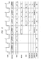
- FIGURE 2 is a timing diagram illustrating the location of instructions obtained from program memory 16 with respect to the various stages of pipeline 20 for an example in which pipeline 20 does not stall.
- processor 12 continuously fetches instructions from locations in program memory 16 having sequential addresses for execution. If for some reason processor 12 stalls, processor 12 continues to fetch instructions from program memory 16. For example, processor 12 may stall while waiting to receive data from data memory 18.
- limited instruction buffer 50 allows accumulation of two instructions while waiting for processing to resume. The operation of prefetch stage 24, fetch stage 26, and decode stage 28 in conjunction with limited instruction buffer 50 is described below with reference to FIGURE 2 for an example in which no stall occurs.
- an address for a memory location corresponding to a first instruction I 1 is calculated.
- an address for a second instruction I 2 is calculated, and fetching of instruction I 1 is initiated.
- an address for a memory location corresponding to a third instruction I 3 is calculated, fetching of instruction I 1 is completed, fetching of I 2 is initiated, and decoding of instruction I 1 is initiated and completed because processor 12 is not stalled.
- register 52 of limited instruction buffer 50 stores instruction I 1 .
- Limited instruction buffer 50 includes a pointer 56 that points to the register in limited instruction buffer 50 that stores the current instruction to be decoded. Instruction pointer 56 is depicted in FIGURE 4 as pointing to register 52.
- pointer 56 points to register 52.
- an address for a fourth instruction I 4 is calculated, fetching of instruction I 2 is completed, fetching of instruction I 3 is initiated, and decoding of instruction I 2 is initiated and completed.
- register 52 continues to store instruction I 1 because instruction I 1 has not been overwritten by another instruction
- register 54 stores instruction I 2
- pointer 56 points to register 54.
- an address for a fifth instruction I 5 is calculated, fetching of instruction I 3 is completed, fetching of instruction I 4 is initiated, and decoding of instruction I 3 is initiated and completed.
- instruction I 3 is stored in register 52 and pointer 56 of limited instruction buffer 50 points to register 52.
- an address for a sixth instruction I 6 is calculated, fetching of instruction I 4 is completed, fetching of instruction I 5 is initiated, decoding of instruction I 4 is initiated and completed, and any data associated with instruction I 3 is read.
- instruction I 4 is stored in register 54 and pointer 56 of limited instruction buffer 50 points to register 54.
- limited instruction buffer 50 stores an instruction in one of its two registers 52, 54 as the instruction is being decoded. Because processor 12 does not stall in the above-described sequence, limited instruction buffer 50 is sufficient to allow continued fetching of additional sequential instructions without reissuing any fetches. Operation of processor 12 during intermittent periods of stalling is described in conjunction with FIGURE 3 .
- FIGURE 3 is a timing diagram illustrating the location of instructions obtained from program memory 16 with respect to various stages of pipeline 20 for an example in which intermittent stalling of pipeline 20 occurs. Operation of prefetch stage 24, fetch stage 26, decode stage 28, and limited instruction buffer 50 is described for the example in which intermittent stalling occurs in pipeline 20.
- an address for a first instruction I 1 is calculated. Stalling of processor 12 does not occur during the first clock cycle, as denoted by the last row of FIGURE 3 .
- an address for a second instruction I 2 is calculated, and fetching of instruction I 1 is initiated.
- stalling of decode stage 28 refers to actual stalling of decode stage 28 or stalling of another stage in pipeline 20 that prevents decode stage 28 from decoding a next instruction. For example, such a stall may occur due to stalling of read stage 30 during a memory read operation.
- instruction I 1 is stored in register 52 and pointer 56 points to register 52.
- decode stage 28 is no longer stalled. Therefore, an address for a fourth instruction I 4 is calculated, fetching of instruction I 3 is completed, and decoding of instruction I 2 is initiated and completed.
- instruction I 3 is stored in register 52
- instruction I 2 is stored in register 54
- pointer 56 points to register 54.
Landscapes
- Engineering & Computer Science (AREA)
- Software Systems (AREA)
- Theoretical Computer Science (AREA)
- Physics & Mathematics (AREA)
- General Engineering & Computer Science (AREA)
- General Physics & Mathematics (AREA)
- Advance Control (AREA)
Claims (9)
- Verfahren zur Zwischenspeicherung von Befehlen in einem Prozessor (12) mit einer Pipeline (20), welche eine Mehrzahl sequenzieller Stufen gefolgt von einer Dekodierungsstufe (28) umfasst, wobei die Pipeline (20) auch einen limitierten Befehlszwischenspeicher (50) mit einer Mehrzahl von Registern (52, 54) umfasst, wobei die Anzahl der Register der Anzahl der Stufen der Pipeline (20) entspricht, welche der Dekodierungsstufe (28) vorangehen, wobei das Verfahren die Schritte umfasst:Speichern eines Zählerstands in einem Programmzähler (58), welcher eine Adresse einer Speicherstelle bezeichnet, welche einen Befehl zum Empfang durch den limitierten Befehlszwischenspeicher (50) speichert;Ermitteln des Betriebszustands der Dekodierungsstufe (28);Setzen des Zählerstands des Zählers (58) in Antwort auf die Ermittlung eines blockierten Zustands der Dekodierungsstufe (28) auf einen Zählerstand, welcher der Adresse der Speicherstelle (16) entspricht, von der ein vorhergehender Befehl abgerufen wurde;Wiederausgabe des vorhergehenden Abrufs des Befehls in einem Speicher (16), bis die Dekodierstufe (28) nicht mehr blockiert ist; undSchreiben des abgerufenen Befehls in ein Register (52, 54) des limitierten Befehlszwischenspeichers (50), nachdem die Dekodierstufe (28) nicht mehr blockiert ist.
- Verfahren nach Anspruch 1, wobei der Schritt des Ermittelns des Betriebszustands der Dekodierstufe (28) eine Bestimmung umfasst, ob der Befehlszwischenspeicher (50) voll ist.
- Verfahren nach Anspruch 2, wobei der Schritt der Wiederausgabe des vorhergegangenen Abrufs eine Wiederhausgabe des vorhergehenden Abrufs eines Befehls, welcher in einem Speicher (16) gespeichert ist, nur dann umfasst, wenn der Befehlszwischenspeicher (50) voll ist.
- Verfahren nach Anspruch 1, wobei der Schritt der Wiederausgabe des vorhergangenen Abrufs einen Abruf eines Befehls umfasst, welcher in einer Speicherstelle (15) gespeichert ist, welche eine Adresse hat, die durch den Zählerstand des Zählers (58) bezeichnet ist.
- Verfahren nach Anspruch 1, wobei der Schritt des Setzens des Zählers ein Anpassen des im Programmzähler (58) gespeicherten Zählerstands umfasst.
- Verfahren nach Anspruch 1, wobei der Schritt des Setzens des Zählers (58) ein Unverändert-Lassen des im Programmzähler gespeicherten Zählerstands (58) umfasst.
- Prozessor Pipeline (20), umfassend:eine Mehrzahl von sequentiellen Stufen (24, 26) gefolgt von einer Dekodierungsstufe (28);einen limitierten Befehlsspeicher (50), welcher betrieben werden kann, um gleichzeitig Befehle zu speichern;ein Zählersystem (58, 60, 62, 64), welches einen Zähler (58) zum Speichern eines Zählerstands beinhaltet, welcher eine Adresse einer Speicherstelle bezeichnet, welche einen Befehl zum Empfang durch den limitierten Befehlsspeicher (50) speichert;wobei die Mehrzahl von sequentiellen Stufen (24, 25) eine Abrufeinheit (26) umfasst, welche betrieben werden kann, um einen Befehl von der durch den Zählerstand bezeichneten Stelle abzurufen;dadurch gekennzeichnet, dassder limitierte Befehlsspeicher (50) betrieben werden kann, um gleichzeitig eine Anzahl von Befehlen zu speichern, die der Anzahl der sequentiellen Stufen (24, 25) der Pipeline (50) vor der Dekodierungsstufe (28) entspricht und nicht mehr;wobei das Zählersystem (58, 60, 62, 64) angeordnet ist, um den Zählerstand des Zählers (58) basierend auf dem Betriebszustand der Dekodierungsstufe (28) zu steuern, wobei bei Ermittlung eines blockierten Zustands der Dekodierungsstufe (28) der Zählerstand des Programmzählers (58) auf einen Zählerstand gesetzt wird, welcher der Adresse der Speicherstelle (16) entspricht, von welcher ein vorhergehender Befehl abgerufen wurde, und bei Ermittlung eines nicht-blockierten Zustands der Dekodierungsstufe (28) der Wert des gegenwärtigen Zählerstands um eins erhöht wird; undMittel zum Schreiben des abgerufenen Befehls in ein Register (52, 54) des limitierten Befehlszwischenspeichers (50), nachdem die Dekodierungsstufe (28) nicht mehr blockiert ist.
- Prozessorpipeline nach Anspruch 7, wobei das Zählersystem (58, 60, 62, 64) ferner einen Multiplexer (60) umfasst, welcher betreibbar ist, um ein Steuersignal (64) zu empfangen, welches hinweisend auf den Betriebszustand der Dekodierungsstufe (28) ist.
- Prozessorpipeline nach Anspruch 8, wobei der Multiplexer (60) betreibbar ist, um den Zählerstand des Zählers (58) und einen erhöhten Zählerstand des Zählers (58) zu empfangen, und ferner betreibbar ist, um ein Ausgangssignal (62) zu erzeugen, welches hinweisend auf entweder den Zählstand des Zählers (58) oder den erhöhten Zählstand des Zählers (58) ist, wobei das Ausgangssignal (62) auf dem Steuersignal (64) basiert, welches hinweisend auf den Betriebszustand der Dekodierungsstufe (28) ist.
Applications Claiming Priority (2)
| Application Number | Priority Date | Filing Date | Title |
|---|---|---|---|
| US09/153,370 US6275924B1 (en) | 1998-09-15 | 1998-09-15 | System for buffering instructions in a processor by reissuing instruction fetches during decoder stall time |
| US153370 | 1998-09-15 |
Publications (3)
| Publication Number | Publication Date |
|---|---|
| EP0987624A2 EP0987624A2 (de) | 2000-03-22 |
| EP0987624A3 EP0987624A3 (de) | 2001-04-25 |
| EP0987624B1 true EP0987624B1 (de) | 2010-08-18 |
Family
ID=22546929
Family Applications (1)
| Application Number | Title | Priority Date | Filing Date |
|---|---|---|---|
| EP99201629A Expired - Lifetime EP0987624B1 (de) | 1998-09-15 | 1999-05-20 | Verfahren und System zum Zwischenspeichern von Befehlen in einem Prozessor |
Country Status (3)
| Country | Link |
|---|---|
| US (1) | US6275924B1 (de) |
| EP (1) | EP0987624B1 (de) |
| DE (1) | DE69942683D1 (de) |
Families Citing this family (8)
| Publication number | Priority date | Publication date | Assignee | Title |
|---|---|---|---|---|
| US7454596B2 (en) * | 2006-06-29 | 2008-11-18 | Intel Corporation | Method and apparatus for partitioned pipelined fetching of multiple execution threads |
| US20080126743A1 (en) * | 2006-07-18 | 2008-05-29 | Via Technologies, Inc. | Reducing Stalls in a Processor Pipeline |
| CN100527075C (zh) * | 2006-07-18 | 2009-08-12 | 威盛电子股份有限公司 | 可减少管线延迟的处理器、管线与指令处理方法 |
| JP5431003B2 (ja) * | 2009-04-03 | 2014-03-05 | スパンション エルエルシー | リコンフィギュラブル回路及びリコンフィギュラブル回路システム |
| US9529594B2 (en) | 2010-11-30 | 2016-12-27 | Oracle International Corporation | Miss buffer for a multi-threaded processor |
| GB2563384B (en) * | 2017-06-07 | 2019-12-25 | Advanced Risc Mach Ltd | Programmable instruction buffering |
| DE102019126666B4 (de) | 2019-10-02 | 2022-06-09 | Honerkamp Industrievertriebs GmbH | Vorrichtung zum Schutz vor einem Wassereinbruch sowie eine Tür oder ein Fenster mit einer solchen Vorrichtung |
| US20230315466A1 (en) * | 2022-04-02 | 2023-10-05 | Eliyah Kilada | Stalling an instruction fetch operation impacted by a hazard without stalling another instruction fetch operation not impacted by the hazard |
Family Cites Families (12)
| Publication number | Priority date | Publication date | Assignee | Title |
|---|---|---|---|---|
| JPS52120640A (en) * | 1976-04-02 | 1977-10-11 | Toshiba Corp | Micro program control system |
| JPS5466048A (en) * | 1977-11-07 | 1979-05-28 | Hitachi Ltd | Information processor |
| JPS5927935B2 (ja) * | 1980-02-29 | 1984-07-09 | 株式会社日立製作所 | 情報処理装置 |
| US4709324A (en) * | 1985-11-27 | 1987-11-24 | Motorola, Inc. | Data processor control unit having an interrupt service using instruction prefetch redirection |
| JPS62152043A (ja) * | 1985-12-26 | 1987-07-07 | Nec Corp | 命令コ−ドアクセス制御方式 |
| US5212777A (en) * | 1989-11-17 | 1993-05-18 | Texas Instruments Incorporated | Multi-processor reconfigurable in single instruction multiple data (SIMD) and multiple instruction multiple data (MIMD) modes and method of operation |
| DE69030648T2 (de) * | 1990-01-02 | 1997-11-13 | Motorola Inc | Verfahren zum sequentiellen Vorabruf von 1-Wort-, 2-Wort oder 3-Wort-Befehlen |
| DE69130588T2 (de) | 1990-05-29 | 1999-05-27 | National Semiconductor Corp., Santa Clara, Calif. | Cache-Speicher von partiell decodierten Befehlen und Verfahren hierfür |
| EP0612013A1 (de) * | 1993-01-21 | 1994-08-24 | Advanced Micro Devices, Inc. | Kombination von Vorausholungspuffer und Befehlscachespeicher |
| US5619663A (en) * | 1994-09-16 | 1997-04-08 | Philips Electronics North America Corp. | Computer instruction prefetch system |
| US5680564A (en) * | 1995-05-26 | 1997-10-21 | National Semiconductor Corporation | Pipelined processor with two tier prefetch buffer structure and method with bypass |
| US5737562A (en) * | 1995-10-06 | 1998-04-07 | Lsi Logic Corporation | CPU pipeline having queuing stage to facilitate branch instructions |
-
1998
- 1998-09-15 US US09/153,370 patent/US6275924B1/en not_active Expired - Lifetime
-
1999
- 1999-05-20 DE DE69942683T patent/DE69942683D1/de not_active Expired - Lifetime
- 1999-05-20 EP EP99201629A patent/EP0987624B1/de not_active Expired - Lifetime
Also Published As
| Publication number | Publication date |
|---|---|
| EP0987624A2 (de) | 2000-03-22 |
| US6275924B1 (en) | 2001-08-14 |
| EP0987624A3 (de) | 2001-04-25 |
| DE69942683D1 (de) | 2010-09-30 |
Similar Documents
| Publication | Publication Date | Title |
|---|---|---|
| US5235686A (en) | Computer system having mixed macrocode and microcode | |
| US5680564A (en) | Pipelined processor with two tier prefetch buffer structure and method with bypass | |
| US5404552A (en) | Pipeline risc processing unit with improved efficiency when handling data dependency | |
| US8171266B2 (en) | Look-ahead load pre-fetch in a processor | |
| JPH1124929A (ja) | 演算処理装置およびその方法 | |
| US6209086B1 (en) | Method and apparatus for fast response time interrupt control in a pipelined data processor | |
| KR20020090107A (ko) | 데이터 처리 장치 내의 루프 버퍼를 이용한 루프 명령처리 장치 | |
| EP2220556B1 (de) | Verfahren und system zur beschleunigung von prozedurrückkehrsequenzen | |
| US6654871B1 (en) | Device and a method for performing stack operations in a processing system | |
| US20250217156A1 (en) | Pipeline protection for cpus with save and restore of intermediate results | |
| US6275903B1 (en) | Stack cache miss handling | |
| JP2742374B2 (ja) | スーパースカラ・プロセッサ・システムにおける命令ディスパッチ効率を向上させる方法およびシステム | |
| EP0987624B1 (de) | Verfahren und System zum Zwischenspeichern von Befehlen in einem Prozessor | |
| US20050102659A1 (en) | Methods and apparatus for setting up hardware loops in a deeply pipelined processor | |
| US5835746A (en) | Method and apparatus for fetching and issuing dual-word or multiple instructions in a data processing system | |
| US6237086B1 (en) | 1 Method to prevent pipeline stalls in superscalar stack based computing systems | |
| EP0496407A2 (de) | Parallelfliessband-Befehlsverarbeitungssystem für sehr lange Befehlswörter | |
| EP0279953B1 (de) | Computersystem mit Durchführung von vermischten Makro- und Mikrocodebefehlen | |
| US6983358B2 (en) | Method and apparatus for maintaining status coherency between queue-separated functional units | |
| JPH06266556A (ja) | データ処理装置 | |
| US6170050B1 (en) | Length decoder for variable length data | |
| EP2278453B1 (de) | Prozessorsystem mit Coprozessor | |
| WO2020214624A1 (en) | Variable latency instructions | |
| KR100632317B1 (ko) | 프로세서에서 명령어들을 버퍼링하기 위한 방법 및 그 시스템 | |
| US20040128476A1 (en) | Scheme to simplify instruction buffer logic supporting multiple strands |
Legal Events
| Date | Code | Title | Description |
|---|---|---|---|
| PUAI | Public reference made under article 153(3) epc to a published international application that has entered the european phase |
Free format text: ORIGINAL CODE: 0009012 |
|
| AK | Designated contracting states |
Kind code of ref document: A2 Designated state(s): DE FR GB IT NL |
|
| AX | Request for extension of the european patent |
Free format text: AL;LT;LV;MK;RO;SI |
|
| PUAL | Search report despatched |
Free format text: ORIGINAL CODE: 0009013 |
|
| AK | Designated contracting states |
Kind code of ref document: A3 Designated state(s): AT BE CH CY DE DK ES FI FR GB GR IE IT LI LU MC NL PT SE |
|
| AX | Request for extension of the european patent |
Free format text: AL;LT;LV;MK;RO;SI |
|
| 17P | Request for examination filed |
Effective date: 20011025 |
|
| AKX | Designation fees paid |
Free format text: DE FR GB IT NL |
|
| 17Q | First examination report despatched |
Effective date: 20071019 |
|
| GRAP | Despatch of communication of intention to grant a patent |
Free format text: ORIGINAL CODE: EPIDOSNIGR1 |
|
| GRAS | Grant fee paid |
Free format text: ORIGINAL CODE: EPIDOSNIGR3 |
|
| GRAA | (expected) grant |
Free format text: ORIGINAL CODE: 0009210 |
|
| AK | Designated contracting states |
Kind code of ref document: B1 Designated state(s): DE FR GB IT NL |
|
| REG | Reference to a national code |
Ref country code: GB Ref legal event code: FG4D |
|
| REF | Corresponds to: |
Ref document number: 69942683 Country of ref document: DE Date of ref document: 20100930 Kind code of ref document: P |
|
| REG | Reference to a national code |
Ref country code: NL Ref legal event code: VDEP Effective date: 20100818 |
|
| PG25 | Lapsed in a contracting state [announced via postgrant information from national office to epo] |
Ref country code: NL Free format text: LAPSE BECAUSE OF FAILURE TO SUBMIT A TRANSLATION OF THE DESCRIPTION OR TO PAY THE FEE WITHIN THE PRESCRIBED TIME-LIMIT Effective date: 20100818 |
|
| PG25 | Lapsed in a contracting state [announced via postgrant information from national office to epo] |
Ref country code: IT Free format text: LAPSE BECAUSE OF FAILURE TO SUBMIT A TRANSLATION OF THE DESCRIPTION OR TO PAY THE FEE WITHIN THE PRESCRIBED TIME-LIMIT Effective date: 20100818 |
|
| PLBE | No opposition filed within time limit |
Free format text: ORIGINAL CODE: 0009261 |
|
| STAA | Information on the status of an ep patent application or granted ep patent |
Free format text: STATUS: NO OPPOSITION FILED WITHIN TIME LIMIT |
|
| 26N | No opposition filed |
Effective date: 20110519 |
|
| REG | Reference to a national code |
Ref country code: DE Ref legal event code: R097 Ref document number: 69942683 Country of ref document: DE Effective date: 20110519 |
|
| PGFP | Annual fee paid to national office [announced via postgrant information from national office to epo] |
Ref country code: GB Payment date: 20140425 Year of fee payment: 16 |
|
| PGFP | Annual fee paid to national office [announced via postgrant information from national office to epo] |
Ref country code: DE Payment date: 20140602 Year of fee payment: 16 Ref country code: FR Payment date: 20140424 Year of fee payment: 16 |
|
| REG | Reference to a national code |
Ref country code: DE Ref legal event code: R119 Ref document number: 69942683 Country of ref document: DE |
|
| GBPC | Gb: european patent ceased through non-payment of renewal fee |
Effective date: 20150520 |
|
| REG | Reference to a national code |
Ref country code: FR Ref legal event code: ST Effective date: 20160129 |
|
| PG25 | Lapsed in a contracting state [announced via postgrant information from national office to epo] |
Ref country code: DE Free format text: LAPSE BECAUSE OF NON-PAYMENT OF DUE FEES Effective date: 20151201 Ref country code: GB Free format text: LAPSE BECAUSE OF NON-PAYMENT OF DUE FEES Effective date: 20150520 |
|
| PG25 | Lapsed in a contracting state [announced via postgrant information from national office to epo] |
Ref country code: FR Free format text: LAPSE BECAUSE OF NON-PAYMENT OF DUE FEES Effective date: 20150601 |