EP0987634A1 - Schnittstellenabtastungselement und kommunikationsvorrichtung die dieses verwendet - Google Patents
Schnittstellenabtastungselement und kommunikationsvorrichtung die dieses verwendet Download PDFInfo
- Publication number
- EP0987634A1 EP0987634A1 EP98923083A EP98923083A EP0987634A1 EP 0987634 A1 EP0987634 A1 EP 0987634A1 EP 98923083 A EP98923083 A EP 98923083A EP 98923083 A EP98923083 A EP 98923083A EP 0987634 A1 EP0987634 A1 EP 0987634A1
- Authority
- EP
- European Patent Office
- Prior art keywords
- terminal
- data
- input
- boundary scan
- boundary
- Prior art date
- Legal status (The legal status is an assumption and is not a legal conclusion. Google has not performed a legal analysis and makes no representation as to the accuracy of the status listed.)
- Granted
Links
Images


Classifications
-
- G—PHYSICS
- G06—COMPUTING OR CALCULATING; COUNTING
- G06F—ELECTRIC DIGITAL DATA PROCESSING
- G06F11/00—Error detection; Error correction; Monitoring
- G06F11/22—Detection or location of defective computer hardware by testing during standby operation or during idle time, e.g. start-up testing
-
- G—PHYSICS
- G01—MEASURING; TESTING
- G01R—MEASURING ELECTRIC VARIABLES; MEASURING MAGNETIC VARIABLES
- G01R31/00—Arrangements for testing electric properties; Arrangements for locating electric faults; Arrangements for electrical testing characterised by what is being tested not provided for elsewhere
- G01R31/28—Testing of electronic circuits, e.g. by signal tracer
- G01R31/317—Testing of digital circuits
- G01R31/3181—Functional testing
- G01R31/3185—Reconfiguring for testing, e.g. LSSD, partitioning
- G01R31/318533—Reconfiguring for testing, e.g. LSSD, partitioning using scanning techniques, e.g. LSSD, Boundary Scan, JTAG
- G01R31/318536—Scan chain arrangements, e.g. connections, test bus, analog signals
-
- G—PHYSICS
- G01—MEASURING; TESTING
- G01R—MEASURING ELECTRIC VARIABLES; MEASURING MAGNETIC VARIABLES
- G01R31/00—Arrangements for testing electric properties; Arrangements for locating electric faults; Arrangements for electrical testing characterised by what is being tested not provided for elsewhere
- G01R31/28—Testing of electronic circuits, e.g. by signal tracer
- G01R31/317—Testing of digital circuits
- G01R31/3181—Functional testing
- G01R31/3185—Reconfiguring for testing, e.g. LSSD, partitioning
- G01R31/318533—Reconfiguring for testing, e.g. LSSD, partitioning using scanning techniques, e.g. LSSD, Boundary Scan, JTAG
- G01R31/318572—Input/Output interfaces
-
- G—PHYSICS
- G01—MEASURING; TESTING
- G01R—MEASURING ELECTRIC VARIABLES; MEASURING MAGNETIC VARIABLES
- G01R31/00—Arrangements for testing electric properties; Arrangements for locating electric faults; Arrangements for electrical testing characterised by what is being tested not provided for elsewhere
- G01R31/28—Testing of electronic circuits, e.g. by signal tracer
- G01R31/2801—Testing of printed circuits, backplanes, motherboards, hybrid circuits or carriers for multichip packages [MCP]
- G01R31/281—Specific types of tests or tests for a specific type of fault, e.g. thermal mapping, shorts testing
- G01R31/2815—Functional tests, e.g. boundary scans, using the normal I/O contacts
-
- Y—GENERAL TAGGING OF NEW TECHNOLOGICAL DEVELOPMENTS; GENERAL TAGGING OF CROSS-SECTIONAL TECHNOLOGIES SPANNING OVER SEVERAL SECTIONS OF THE IPC; TECHNICAL SUBJECTS COVERED BY FORMER USPC CROSS-REFERENCE ART COLLECTIONS [XRACs] AND DIGESTS
- Y02—TECHNOLOGIES OR APPLICATIONS FOR MITIGATION OR ADAPTATION AGAINST CLIMATE CHANGE
- Y02P—CLIMATE CHANGE MITIGATION TECHNOLOGIES IN THE PRODUCTION OR PROCESSING OF GOODS
- Y02P70/00—Climate change mitigation technologies in the production process for final industrial or consumer products
- Y02P70/50—Manufacturing or production processes characterised by the final manufactured product
Definitions
- the boundary scan testing method can be implemented for semiconductor integrated circuits ( IC chips ) in which the boundary scan elements are integrated.
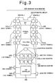
- the boundary scan element is composed, for example, of a plurality of boundary cells 214, each of which is individually provided between an input/output terminal of an internal logic circuit 211 for allowing an integrated circuit 210 to achieve its inherent function and an input terminal 212 of the integrated circuit 210 as well as between the input/output terminal of the internal logic circuit 211 and an output terminal 213 of the integrated circuit 210; a TAP controller (TAP circuit) 219 for controlling input/output of data to/from each boundary cell 214; a TDI terminal 220 for receiving test data; a TDO terminal 221 for transmitting the test data; a TCK terminal 122 to which a clock signal is inputted; and a TMS terminal 223 for receiving a mode signal to switch an operation mode of the TAP controller 219.
- TAP controller TAP circuit
- the boundary scan element may optionally be provided with any of a bypass register 215; an ID CODE register 216; an instruction register 217; and a TRS terminal 22 for receiving a reset signal.
- the bypass register 215 serves to transfer communication data without allowing the communication data to pass through the boundary cells
- the ID CODE register 216 serves to discriminate sources of the communication data by outputting individually assigned ID CODEs.
- the instruction register 217 serves to decode specified data selected among the communication data so as to perform a transition of the operation mode independently of a TMS signal. It should be noted that the bypass register 215, the ID CODE register 216 and the instruction register 217 are called a boundary scan register (118).
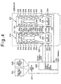
- the boundary scan elements incorporated in the plurality of integrated circuits 210 are connected in series. Specifically, the TDO terminal 221 of the first integrated circuit 210 shown in the left in Fig. 4 and the TDI terminal 220 of the second integrated circuit 210 shown in the right in Fig. 4 are connected. Moreover, an output terminal 229 of a boundary scan controller board 228 provided in a host computer unit 227 is connected to the TDI terminal 220 of the first integrated circuit 210, and an input terminal 230 of the boundary scan controller board 228 is connected to the TDO terminal 221 of the second integrated circuit 210.
- the test procedures are as follows.
- each output terminal 213 is inputted, via each printed pattern 233 constituting a system bus and the like, to corresponding one of the input terminals 212 of the second integrated circuit 210. Moreover, the data is taken into each boundary cell 214 provided for corresponding one of the input terminals 212.
- Each of the boundary scan elements 243a to 243c functions in synchronization with clock signals transmitted from the TCK terminal 241d of the communication controller unit 241, and an operation mode of each TAP controller is switched by a TMS signal transmitted from the TMS terminal 241c of the communication controller unit 241.
- the communication controller unit 57 has a hardware circuit, a microprocessor circuit and the like, and transmits a necessary signal from a TMS terminal 57e or 57f and the TCK terminal 57g or 57h to the TMS terminal 108 and TCK terminal 109 of the boundary scan elements 100a to 100d via a TMS communication line 70 and a TCK communication line 71, based on instruction contents outputted from the host computer unit 6.
- the communication controller unit 57 thus drives the boundary scan elements 100a to 100d.
- the communication controller unit 57 and the clockwise and counterclockwise combinations are connected so that the transfer direction of the communication data in the clockwise combination of the boundary scan elements 100a to 100d is inverse to the transfer direction of the communication data in the counterclockwise combination.
Landscapes
- Engineering & Computer Science (AREA)
- General Engineering & Computer Science (AREA)
- Physics & Mathematics (AREA)
- General Physics & Mathematics (AREA)
- Theoretical Computer Science (AREA)
- Quality & Reliability (AREA)
- Computer Hardware Design (AREA)
- Tests Of Electronic Circuits (AREA)
- Control Of Indicators Other Than Cathode Ray Tubes (AREA)
- Test And Diagnosis Of Digital Computers (AREA)
- Absorbent Articles And Supports Therefor (AREA)
- Orthopedics, Nursing, And Contraception (AREA)
- Semiconductor Integrated Circuits (AREA)
- Communication Control (AREA)
Applications Claiming Priority (3)
| Application Number | Priority Date | Filing Date | Title |
|---|---|---|---|
| JP14380497 | 1997-06-02 | ||
| JP14380497 | 1997-06-02 | ||
| PCT/JP1998/002432 WO1998055927A1 (fr) | 1997-06-02 | 1998-06-02 | Element de test peripherique et equipement de communication utilisant ledit element |
Publications (3)
| Publication Number | Publication Date |
|---|---|
| EP0987634A1 true EP0987634A1 (de) | 2000-03-22 |
| EP0987634A4 EP0987634A4 (de) | 2002-10-09 |
| EP0987634B1 EP0987634B1 (de) | 2006-08-09 |
Family
ID=15347376
Family Applications (3)
| Application Number | Title | Priority Date | Filing Date |
|---|---|---|---|
| EP98921883A Expired - Lifetime EP0987632B1 (de) | 1997-06-02 | 1998-05-29 | Schnittstellenabtastungselement und kommunikationsvorrichtung die dieses verwendet |
| EP98923061A Expired - Lifetime EP0987633B8 (de) | 1997-06-02 | 1998-06-01 | Kommunikationssystem |
| EP98923083A Expired - Lifetime EP0987634B1 (de) | 1997-06-02 | 1998-06-02 | Schnittstellenabtastungselement und kommunikationsvorrichtung die dieses verwendet |
Family Applications Before (2)
| Application Number | Title | Priority Date | Filing Date |
|---|---|---|---|
| EP98921883A Expired - Lifetime EP0987632B1 (de) | 1997-06-02 | 1998-05-29 | Schnittstellenabtastungselement und kommunikationsvorrichtung die dieses verwendet |
| EP98923061A Expired - Lifetime EP0987633B8 (de) | 1997-06-02 | 1998-06-01 | Kommunikationssystem |
Country Status (7)
| Country | Link |
|---|---|
| US (3) | US6658614B1 (de) |
| EP (3) | EP0987632B1 (de) |
| JP (3) | JP4012577B2 (de) |
| KR (3) | KR100454989B1 (de) |
| CA (4) | CA2291681C (de) |
| DE (3) | DE69832605T2 (de) |
| WO (3) | WO1998055926A1 (de) |
Families Citing this family (24)
| Publication number | Priority date | Publication date | Assignee | Title |
|---|---|---|---|---|
| JP3401523B2 (ja) * | 1999-01-11 | 2003-04-28 | デュアキシズ株式会社 | 通信素子及びこれを用いた通信装置 |
| US7058862B2 (en) * | 2000-05-26 | 2006-06-06 | Texas Instruments Incorporated | Selecting different 1149.1 TAP domains from update-IR state |
| US7003707B2 (en) | 2000-04-28 | 2006-02-21 | Texas Instruments Incorporated | IC tap/scan test port access with tap lock circuitry |
| US20010037479A1 (en) * | 2000-04-28 | 2001-11-01 | Whetsel Lee D. | Selectable dual mode test access port method and apparatus |
| US6934898B1 (en) * | 2001-11-30 | 2005-08-23 | Koninklijke Philips Electronics N.V. | Test circuit topology reconfiguration and utilization techniques |
| US20050201340A1 (en) * | 2002-05-13 | 2005-09-15 | Xudong Wang | Distributed TDMA for wireless mesh network |
| US7941149B2 (en) | 2002-05-13 | 2011-05-10 | Misonimo Chi Acquistion L.L.C. | Multi-hop ultra wide band wireless network communication |
| US7957356B2 (en) | 2002-05-13 | 2011-06-07 | Misomino Chi Acquisitions L.L.C. | Scalable media access control for multi-hop high bandwidth communications |
| US7835372B2 (en) * | 2002-05-13 | 2010-11-16 | Weilin Wang | System and method for transparent wireless bridging of communication channel segments |
| US20040229566A1 (en) * | 2003-05-13 | 2004-11-18 | Weilin Wang | Systems and methods for congestion control in a wireless mesh network |
| US7069483B2 (en) * | 2002-05-13 | 2006-06-27 | Kiyon, Inc. | System and method for identifying nodes in a wireless mesh network |
| US7852796B2 (en) * | 2002-05-13 | 2010-12-14 | Xudong Wang | Distributed multichannel wireless communication |
| US8780770B2 (en) | 2002-05-13 | 2014-07-15 | Misonimo Chi Acquisition L.L.C. | Systems and methods for voice and video communication over a wireless network |
| US20050201346A1 (en) * | 2003-05-13 | 2005-09-15 | Weilin Wang | Systems and methods for broadband data communication in a wireless mesh network |
| WO2004068156A1 (en) * | 2003-01-28 | 2004-08-12 | Koninklijke Philips Electronics N.V. | Boundary scan circuit with integrated sensor for sensing physical operating parameters |
| US8175613B2 (en) * | 2006-08-04 | 2012-05-08 | Misonimo Chi Acquisitions L.L.C. | Systems and methods for determining location of devices within a wireless network |
| US8040857B2 (en) * | 2006-12-07 | 2011-10-18 | Misonimo Chi Acquisitions L.L.C. | System and method for timeslot and channel allocation |
| GB0712373D0 (en) * | 2007-06-26 | 2007-08-01 | Astrium Ltd | Embedded test system and method |
| US20100031077A1 (en) * | 2008-07-29 | 2010-02-04 | Swoboda Gary L | Alternate Signaling Mechanism Using Clock and Data |
| US8331163B2 (en) * | 2010-09-07 | 2012-12-11 | Infineon Technologies Ag | Latch based memory device |
| US8880968B2 (en) * | 2011-04-26 | 2014-11-04 | Texas Instruments Incorporated | Interposer having functional leads, TAP, trigger unit, and monitor circuitry |
| US9208571B2 (en) | 2011-06-06 | 2015-12-08 | Microsoft Technology Licensing, Llc | Object digitization |
| CN110659037B (zh) * | 2019-09-25 | 2021-03-09 | 苏州浪潮智能科技有限公司 | 一种基于jtag的烧录装置 |
| JP7518408B2 (ja) | 2022-08-23 | 2024-07-18 | 東芝情報システム株式会社 | 半導体テスト装置及び半導体テスト方法 |
Family Cites Families (23)
| Publication number | Priority date | Publication date | Assignee | Title |
|---|---|---|---|---|
| JPH0690260B2 (ja) | 1986-05-30 | 1994-11-14 | 三菱電機株式会社 | 論理回路試験装置 |
| JPS6468843A (en) | 1987-09-10 | 1989-03-14 | Matsushita Electric Industrial Co Ltd | Test mode setting circuit |
| JPH01229982A (ja) * | 1988-03-10 | 1989-09-13 | Fujitsu Ltd | スキャン試験方式 |
| US4989209A (en) | 1989-03-24 | 1991-01-29 | Motorola, Inc. | Method and apparatus for testing high pin count integrated circuits |
| US5130988A (en) * | 1990-09-17 | 1992-07-14 | Northern Telecom Limited | Software verification by fault insertion |
| US5132635A (en) * | 1991-03-05 | 1992-07-21 | Ast Research, Inc. | Serial testing of removable circuit boards on a backplane bus |
| JPH04281691A (ja) | 1991-03-11 | 1992-10-07 | Sony Corp | デジタル信号処理回路の自己診断装置 |
| US5325368A (en) * | 1991-11-27 | 1994-06-28 | Ncr Corporation | JTAG component description via nonvolatile memory |
| US5377198A (en) * | 1991-11-27 | 1994-12-27 | Ncr Corporation (Nka At&T Global Information Solutions Company | JTAG instruction error detection |
| US5400345A (en) * | 1992-03-06 | 1995-03-21 | Pitney Bowes Inc. | Communications system to boundary-scan logic interface |
| JPH05273311A (ja) * | 1992-03-24 | 1993-10-22 | Nec Corp | 論理集積回路 |
| US5617420A (en) | 1992-06-17 | 1997-04-01 | Texas Instrument Incorporated | Hierarchical connection method, apparatus, and protocol |
| JP2960261B2 (ja) | 1992-07-04 | 1999-10-06 | 三洋化成工業株式会社 | 汚泥脱水剤 |
| US5450415A (en) * | 1992-11-25 | 1995-09-12 | Matsushita Electric Industrial Co., Ltd. | Boundary scan cell circuit and boundary scan test circuit |
| US5333139A (en) * | 1992-12-30 | 1994-07-26 | Intel Corporation | Method of determining the number of individual integrated circuit computer chips or the like in a boundary scan test chain and the length of the chain |
| AU6250794A (en) * | 1993-02-25 | 1994-09-14 | Reticular Systems, Inc. | Real-time rule based processing system |
| JPH06300821A (ja) | 1993-04-14 | 1994-10-28 | Nec Corp | コントローラ内蔵のlsi |
| US5544309A (en) * | 1993-04-22 | 1996-08-06 | International Business Machines Corporation | Data processing system with modified planar for boundary scan diagnostics |
| US5535222A (en) * | 1993-12-23 | 1996-07-09 | At&T Corp. | Method and apparatus for controlling a plurality of systems via a boundary-scan port during testing |
| JPH08233904A (ja) | 1995-02-27 | 1996-09-13 | Nec Eng Ltd | バウンダリスキャン回路 |
| US5487074A (en) * | 1995-03-20 | 1996-01-23 | Cray Research, Inc. | Boundary scan testing using clocked signal |
| JPH0915299A (ja) | 1995-06-27 | 1997-01-17 | Nec Eng Ltd | バウンダリスキャン回路およびこれを用いた集積 回路 |
| US5862152A (en) * | 1995-11-13 | 1999-01-19 | Motorola, Inc. | Hierarchically managed boundary-scan testable module and method |
-
1998
- 1998-05-29 US US09/424,454 patent/US6658614B1/en not_active Expired - Fee Related
- 1998-05-29 CA CA002291681A patent/CA2291681C/en not_active Expired - Fee Related
- 1998-05-29 KR KR10-1999-7011187A patent/KR100454989B1/ko not_active Expired - Fee Related
- 1998-05-29 WO PCT/JP1998/002383 patent/WO1998055926A1/ja not_active Ceased
- 1998-05-29 CA CA002485309A patent/CA2485309A1/en not_active Abandoned
- 1998-05-29 EP EP98921883A patent/EP0987632B1/de not_active Expired - Lifetime
- 1998-05-29 DE DE69832605T patent/DE69832605T2/de not_active Expired - Fee Related
- 1998-05-29 JP JP50204099A patent/JP4012577B2/ja not_active Expired - Fee Related
- 1998-06-01 DE DE69833320T patent/DE69833320T2/de not_active Expired - Fee Related
- 1998-06-01 KR KR1019997010996A patent/KR100316000B1/ko not_active Expired - Fee Related
- 1998-06-01 JP JP50411699A patent/JP3984300B2/ja not_active Expired - Lifetime
- 1998-06-01 WO PCT/JP1998/002404 patent/WO1998058317A1/ja not_active Ceased
- 1998-06-01 EP EP98923061A patent/EP0987633B8/de not_active Expired - Lifetime
- 1998-06-01 CA CA002292771A patent/CA2292771C/en not_active Expired - Fee Related
- 1998-06-01 US US09/424,453 patent/US6671840B1/en not_active Expired - Fee Related
- 1998-06-02 KR KR1019997011188A patent/KR100315999B1/ko not_active Expired - Fee Related
- 1998-06-02 CA CA002291682A patent/CA2291682C/en not_active Expired - Fee Related
- 1998-06-02 EP EP98923083A patent/EP0987634B1/de not_active Expired - Lifetime
- 1998-06-02 WO PCT/JP1998/002432 patent/WO1998055927A1/ja not_active Ceased
- 1998-06-02 JP JP50205099A patent/JP3936747B2/ja not_active Expired - Fee Related
- 1998-06-02 US US09/424,455 patent/US6701475B1/en not_active Expired - Fee Related
- 1998-06-02 DE DE69835517T patent/DE69835517T2/de not_active Expired - Fee Related
Also Published As
Similar Documents
| Publication | Publication Date | Title |
|---|---|---|
| EP0987634B1 (de) | Schnittstellenabtastungselement und kommunikationsvorrichtung die dieses verwendet | |
| JPWO1998055927A1 (ja) | バウンダリスキャン素子及びこれを用いた通信装置 | |
| JPWO1998055926A1 (ja) | バウンダリスキャン素子及びこれを用いた通信装置 | |
| EP0444845A1 (de) | Halbleitervorrichtung mit integrierter Halbleiterschaltung und Betriebsverfahren dafür | |
| EP0470803A2 (de) | Durch Ereignis befähigte Prüfarchitektur | |
| US20040068675A1 (en) | Circuit board having boundary scan self-testing function | |
| US9810739B2 (en) | Electronic system, system diagnostic circuit and operation method thereof | |
| EP0849678A2 (de) | System und Verfahren zur Prüfung elektronischer Geräte | |
| US7174492B1 (en) | AC coupled line testing using boundary scan test methodology | |
| KR100316001B1 (ko) | 통신장치 | |
| EP1136832A2 (de) | Prüfsystem und Prüfverfahren zur überwachten Einbrennung von Mikrocomputer | |
| US6813737B1 (en) | Short circuited capacitor detection in AC coupled links using boundary scan test methodology | |
| KR100697264B1 (ko) | 딜레이 체인 회로를 이용한 반도체 장치의 테스트 회로 및그의 테스트 방법 | |
| JPWO1998055925A1 (ja) | 通信装置 | |
| JPWO1998058317A1 (ja) | 通信装置 | |
| JP2003315423A (ja) | 半導体集積回路 | |
| KR20050063998A (ko) | 멀티 프로세서 시스템에서의 전원 제어 장치 및 그를이용한 프로세서 테스트 장치 |
Legal Events
| Date | Code | Title | Description |
|---|---|---|---|
| PUAI | Public reference made under article 153(3) epc to a published international application that has entered the european phase |
Free format text: ORIGINAL CODE: 0009012 |
|
| 17P | Request for examination filed |
Effective date: 19991214 |
|
| AK | Designated contracting states |
Kind code of ref document: A1 Designated state(s): DE FR GB IT |
|
| D17D | Deferred search report published (deleted) | ||
| A4 | Supplementary search report drawn up and despatched |
Effective date: 20020827 |
|
| AK | Designated contracting states |
Kind code of ref document: A4 Designated state(s): DE FR GB IT |
|
| RIC1 | Information provided on ipc code assigned before grant |
Free format text: 7G 06F 11/22 A, 7G 01R 31/28 B, 7G 01R 31/3185 B |
|
| 17Q | First examination report despatched |
Effective date: 20030512 |
|
| GRAP | Despatch of communication of intention to grant a patent |
Free format text: ORIGINAL CODE: EPIDOSNIGR1 |
|
| RAP1 | Party data changed (applicant data changed or rights of an application transferred) |
Owner name: NAGOYA, MITSUGU Owner name: KOKEN CO., LTD. |
|
| GRAS | Grant fee paid |
Free format text: ORIGINAL CODE: EPIDOSNIGR3 |
|
| RAP1 | Party data changed (applicant data changed or rights of an application transferred) |
Owner name: NAGOYA, MITSUGU Owner name: KOKEN CO., LTD. |
|
| RAP1 | Party data changed (applicant data changed or rights of an application transferred) |
Owner name: DUAXES CORPORATION |
|
| GRAA | (expected) grant |
Free format text: ORIGINAL CODE: 0009210 |
|
| AK | Designated contracting states |
Kind code of ref document: B1 Designated state(s): DE FR GB IT |
|
| PG25 | Lapsed in a contracting state [announced via postgrant information from national office to epo] |
Ref country code: IT Free format text: LAPSE BECAUSE OF FAILURE TO SUBMIT A TRANSLATION OF THE DESCRIPTION OR TO PAY THE FEE WITHIN THE PRESCRIBED TIME-LIMIT;WARNING: LAPSES OF ITALIAN PATENTS WITH EFFECTIVE DATE BEFORE 2007 MAY HAVE OCCURRED AT ANY TIME BEFORE 2007. THE CORRECT EFFECTIVE DATE MAY BE DIFFERENT FROM THE ONE RECORDED. Effective date: 20060809 |
|
| REG | Reference to a national code |
Ref country code: GB Ref legal event code: FG4D |
|
| REF | Corresponds to: |
Ref document number: 69835517 Country of ref document: DE Date of ref document: 20060921 Kind code of ref document: P |
|
| ET | Fr: translation filed | ||
| PLBE | No opposition filed within time limit |
Free format text: ORIGINAL CODE: 0009261 |
|
| STAA | Information on the status of an ep patent application or granted ep patent |
Free format text: STATUS: NO OPPOSITION FILED WITHIN TIME LIMIT |
|
| 26N | No opposition filed |
Effective date: 20070510 |
|
| PGFP | Annual fee paid to national office [announced via postgrant information from national office to epo] |
Ref country code: IT Payment date: 20080626 Year of fee payment: 11 |
|
| PGFP | Annual fee paid to national office [announced via postgrant information from national office to epo] |
Ref country code: DE Payment date: 20080612 Year of fee payment: 11 |
|
| PGFP | Annual fee paid to national office [announced via postgrant information from national office to epo] |
Ref country code: FR Payment date: 20080606 Year of fee payment: 11 |
|
| PGFP | Annual fee paid to national office [announced via postgrant information from national office to epo] |
Ref country code: GB Payment date: 20080603 Year of fee payment: 11 |
|
| GBPC | Gb: european patent ceased through non-payment of renewal fee |
Effective date: 20090602 |
|
| REG | Reference to a national code |
Ref country code: FR Ref legal event code: ST Effective date: 20100226 |
|
| PG25 | Lapsed in a contracting state [announced via postgrant information from national office to epo] |
Ref country code: FR Free format text: LAPSE BECAUSE OF NON-PAYMENT OF DUE FEES Effective date: 20090630 |
|
| PG25 | Lapsed in a contracting state [announced via postgrant information from national office to epo] |
Ref country code: GB Free format text: LAPSE BECAUSE OF NON-PAYMENT OF DUE FEES Effective date: 20090602 |
|
| PG25 | Lapsed in a contracting state [announced via postgrant information from national office to epo] |
Ref country code: DE Free format text: LAPSE BECAUSE OF NON-PAYMENT OF DUE FEES Effective date: 20100101 |
|
| PG25 | Lapsed in a contracting state [announced via postgrant information from national office to epo] |
Ref country code: IT Free format text: LAPSE BECAUSE OF NON-PAYMENT OF DUE FEES Effective date: 20090602 |