EP0987774A2 - Electrode avec injection des trous améliorée - Google Patents
Electrode avec injection des trous améliorée Download PDFInfo
- Publication number
- EP0987774A2 EP0987774A2 EP99104907A EP99104907A EP0987774A2 EP 0987774 A2 EP0987774 A2 EP 0987774A2 EP 99104907 A EP99104907 A EP 99104907A EP 99104907 A EP99104907 A EP 99104907A EP 0987774 A2 EP0987774 A2 EP 0987774A2
- Authority
- EP
- European Patent Office
- Prior art keywords
- layer
- ito
- tin oxide
- oled
- indium tin
- Prior art date
- Legal status (The legal status is an assumption and is not a legal conclusion. Google has not performed a legal analysis and makes no representation as to the accuracy of the status listed.)
- Withdrawn
Links
Images




Classifications
-
- H—ELECTRICITY
- H10—SEMICONDUCTOR DEVICES; ELECTRIC SOLID-STATE DEVICES NOT OTHERWISE PROVIDED FOR
- H10K—ORGANIC ELECTRIC SOLID-STATE DEVICES
- H10K59/00—Integrated devices, or assemblies of multiple devices, comprising at least one organic light-emitting element covered by group H10K50/00
- H10K59/30—Devices specially adapted for multicolour light emission
- H10K59/32—Stacked devices having two or more layers, each emitting at different wavelengths
-
- H—ELECTRICITY
- H10—SEMICONDUCTOR DEVICES; ELECTRIC SOLID-STATE DEVICES NOT OTHERWISE PROVIDED FOR
- H10K—ORGANIC ELECTRIC SOLID-STATE DEVICES
- H10K59/00—Integrated devices, or assemblies of multiple devices, comprising at least one organic light-emitting element covered by group H10K50/00
- H10K59/80—Constructional details
- H10K59/805—Electrodes
- H10K59/8051—Anodes
-
- H—ELECTRICITY
- H10—SEMICONDUCTOR DEVICES; ELECTRIC SOLID-STATE DEVICES NOT OTHERWISE PROVIDED FOR
- H10K—ORGANIC ELECTRIC SOLID-STATE DEVICES
- H10K85/00—Organic materials used in the body or electrodes of devices covered by this subclass
- H10K85/30—Coordination compounds
- H10K85/321—Metal complexes comprising a group IIIA element, e.g. Tris (8-hydroxyquinoline) gallium [Gaq3]
- H10K85/324—Metal complexes comprising a group IIIA element, e.g. Tris (8-hydroxyquinoline) gallium [Gaq3] comprising aluminium, e.g. Alq3
-
- H—ELECTRICITY
- H10—SEMICONDUCTOR DEVICES; ELECTRIC SOLID-STATE DEVICES NOT OTHERWISE PROVIDED FOR
- H10K—ORGANIC ELECTRIC SOLID-STATE DEVICES
- H10K85/00—Organic materials used in the body or electrodes of devices covered by this subclass
- H10K85/60—Organic compounds having low molecular weight
- H10K85/631—Amine compounds having at least two aryl rest on at least one amine-nitrogen atom, e.g. triphenylamine
Definitions
- the present invention relates to organic light emitting devices (OLEDs), and more particularly to an improved electrode for use in such devices.
- OLEDs are comprised of one or more organic layers in which one of the layers is comprised of an organic material that can be made to electroluminesce, by applying a voltage across the device.
- Certain OLEDs have been shown to have sufficient brightness, range of color and operating lifetimes for use as a practical alternative technology to LCD-based full color flat-panel displays. S.R. Forrest, P.E. Burrows and M.E. Thompson, Laser Focus World, Feb. 1995.
- Figure 1 shows a double heterostructure OLED 100.
- An anode 110, a hole transporting layer (HTL) 120, an emissive layer (EL) 130, an electron transporting layer (ETL) 140, and a cathode 150 are stacked in that order.
- HTL hole transporting layer
- EL emissive layer
- ETL electron transporting layer
- cathode 150 When a voltage is applied between anode 110 and cathode 150, current flows from anode 110, across HTL 120, to EL 130, primarily by conduction of holes traveling from anode 110 to EL 130.
- Holes are injected into EL 130 by HTL 120, and electrons are injected into EL 130 by ETL 140.
- the electrons and holes combine to form excitons in EL 130, which then decay preferentially by a photo
- FIG. 2 shows a single heterostructure OLED 200.
- An anode 210, a hole transporting layer (HTL) 220, an emissive layer (EL) 230, and a cathode 240 are stacked in that order.
- a single heterostructure OLED functions in a manner similar to a double heterostructure OLED, except that the EL also functions as a transport layer.
- EL 230 also functions as an ETL.
- HTL 220 injects holes into EL 230. The electrons and holes combine to form excitons in EL 230, which then decay preferentially by a photoemissive mechanism to emit light.
- Figure 3 shows a single layer OLED 300.
- An anode 310, an emissive layer (EL) 320, and a cathode 330 are stacked in that order.
- a single layer OLED functions in a manner similar to a double or single heterostructure OLED, except that the EL also functions as an HTL and an ETL.
- a voltage is applied between anode 310 and cathode 330, current flows across EL 320, primarily by the conduction of electrons injected by cathode 330 and holes injected by anode 310.
- the electrons and holes combine to form excitons in EL 320, which then decay preferentially by a photoemissive mechanism to emit light.
- Transparent OLEDs TOLEDs
- SOLEDs stacked OLEDs
- the TOLED had greater than 71% transparency when turned off and emitted light from both top and bottom device surfaces with high efficiency (approaching 1% quantum efficiency) when the device was turned on. Because they are transparent, TOLEDs can be stacked, and the light emitted by each TOLED in the stack can pass through the other TOLEDs.
- U.S. Patent No. 5,703,436, Forrest et al. discloses a SOLED having independently addressable stacked red, green, and blue OLEDs.
- Such a stack represents a significant step towards a high-resolution R-G-B pixel.
- An electrode having an Mg-Ag layer and an ITO layer was used between the OLEDs in the stack, where the Mg-Ag layer served as an electron injecting layer for one of the OLEDs contacting the electrode, and the ITO layer served as a hole injecting electrode for the other OLED.
- Each layer in the SOLED was independently addressable and emitted its own characteristic color, red, green, or blue. This colored emission could be transmitted through other OLEDs in the stack and the glass substrate, thus allowing the device to emit any color that could be produced by varying the relative output of the red, green, and blue color-emitting layers.
- U.S. Patent No. 5,707,745, Forrest et al. which is incorporated herein by reference, disclosed an integrated SOLED having red, green and blue OLEDs in a stack, each independently controllable, such that the color and intensity of the SOLED can be independently varied.
- Such a SOLED provides a pixel suitable for use in a color display that has a compact pixel size relative to pixels that rely on three OLEDs side-by-side to achieve independently controllable red, green and blue emission.
- This compact pixel size enables high resolution, full color integrated pixels.
- relatively low cost fabrication techniques as compared with prior art methods, may be utilized for making such devices.
- ITO indium tin oxide
- U.S. Patent Nos. 5,707,745 and 5,703,436 to Forrest et al. which are incorporated by reference.
- ITO is a preferred electrode material because electrodes made of ITO may be made to transmit a large fraction of light in the visible spectrum, and to correspondingly absorb and/or reflect only a small fraction of light in the visible spectrum. As a result, a large fraction of the light emitted by an OLED having ITO electrodes reaches the viewer. Also, undesirable microcavity effects caused by reflective electrodes may be minimized by using ITO electrodes.
- Substrates pre-coated with ITO can be purchased, for example, from Donnelly Applied Films Corp., located in Boulder, Colorado. ITO can be deposited by a variety of methods, such as sputtering, thermal evaporation, chemical vapor deposition and spray pyrolysis. Moreover, ITO electrodes can be deposited on top of organic thin films without significantly damaging the thin film. For example, ITO can be deposited onto an organic thin film using a room temperature, low power, RF magnetron sputtering process, without significantly damaging to the organic thin film, as disclosed in U.S. Patent Application 08/928,800 (filed September 12, 1997), which is incorporated by reference.
- An ITO layer may also be incorporated into an electrode that comprises multiple layers, as disclosed in Burrows et al., Color-tunable organic light emitting devices , Appl. Phys. Lett. 69 (20), 2959 (1996).
- an electrode may comprise a very thin (about 100 ⁇ ) layer of metal(s) covered with a transparent conducting oxide thin film, such as ITO.
- the present invention provides a method of fabricating an organic light emitting device.
- a layer of indium tin oxide is deposited. While the layer of indium tin oxide is being deposited, a controlled amount of additional oxygen is incorporated into a surface of the layer of indium tin oxide. An organic layer is then deposited onto the surface.
- the present invention further provides an organic light emitting device having an anode, a cathode, and an organic layer.
- the anode has a surface into which additional oxygen was incorporated during fabrication.
- the organic layer is disposed between the anode and the cathode, and is in direct contact with the surface.
- the present invention achieves a low operating voltage, high quantum efficiency SOLED by incorporating additional oxygen during fabrication into a surface of an ITO anode that contacts an organic layer.
- the "surface" of an electrode refers to a portion of the electrode, where the oxygen content of the portion has an effect on the injection of charge carriers into an adjacent organic layer. This "surface” may extend into the electrode. For example, the surface may extend to a depth of 60 ⁇ or more away from the adjacent organic layer.
- additional oxygen refers to an amount oxygen in excess of the amount in the bulk ITO, i.e. , ITO not at the "surface" of the electrode.
- the organic layer into which holes are injected from the anode may be a hole transporting layer of a single or double heterostructure OLED, an emissive layer of a single heterostructure or single layer OLED, or another type of organic layer, such as a hole injection enhancement layer.
- SOLEDs having anodes fabricated in accordance with the present invention exhibit performance superior to that of previously demonstrated SOLEDs.
- the high drive voltages and inefficient light emission are caused in part by poor hole injection from the ITO anode into the organic layers.
- incorporating additional oxygen into the surface of the ITO anode the injection of holes into the organic layers is improved.
- the additional oxygen shifts the Fermi level of the ITO, resulting in better alignment between the Fermi level of the ITO and the Highest Occupied Molecular Orbital (HOMO) level of the organic material subsequently deposited onto the ITO, for many organic materials used to fabricate OLEDs.
- HOMO Highest Occupied Molecular Orbital
- the energy barrier for holes jumping from the ITO into an adjacent organic layer is lowered, and hole injection from the ITO into the organic layer is improved.
- incorporating additional oxygen into ITO lowers the conductivity, due to a decrease in the concentration holes associated with oxygen vacancies, as disclosed by Fan et al., X-ray photoemission spectroscopy studies of Sn- doped indium-oxide films , J. App. Phys. 48 (8), 3524 (1977), which is incorporated by reference.
- a decrease in conductivity may increase drive voltage and decrease efficiency.
- the oxygen content throughout an ITO electrode affects conductivity, while the oxygen content at the surface affects hole injection properties. As a result, it is preferable to incorporate the oxygen into the surface of the electrode, which results in enhanced hole injection, but not into the rest of the electrode, to minimize any decrease in conductivity.
- the oxygen content of an ITO anode is controlled using a modified sputtering process.
- oxygen gas is introduced into the sputtering gas at controlled times and in a controlled amount
- a 600 ⁇ ITO electrode could be sputter deposited using an Ar flow of 150 sccm with no oxygen gas during the deposition of the first 540 ⁇ , with 0.1 sccm oxygen gas during the next 50 ⁇ , and with 0.2 sccm oxygen gas during the last 10 ⁇ .
- the amount and distribution of oxygen in the ITO can be controlled with a great deal of precision, because the additional oxygen is incorporated into the surface of the ITO anode while the anode is being deposited.
- the organic layer into which holes are to be injected may then be deposited onto that surface of the anode, preferably without exposure to atmosphere.
- the depth of the ITO surface and the oxygen distribution within that surface may be varied from the specific examples disclosed. For example, such variations may depend upon the specific organic materials used and the various size parameters of the device.
- the oxygen content of an ITO electrode is controlled by using oxygen-rich targets during a portion of the step of depositing a layer of indium tin oxide.
- target refers to a source of material used for depositing the ITO electrode.
- an ITO electrode may be deposited from one or more targets of indium oxide (In 2 O 3 ), tin oxide (SnO, Sn 2 O 3 , and/or SnO 2 ), ITO, and combinations thereof
- the oxygen content of a target may be controlled by selecting the oxidation state of the tin oxide in the target, as well as the concentration of oxygen vacancies in the oxides.
- Targets having a higher oxygen content are "oxygen-rich" relative to targets having a lower oxygen content.
- the oxygen content of the electrode may be controlled.
- the ITO electrode may be deposited by co-deposition from an oxygen-rich target and an oxygen-poor target, where the percentage of the co-deposition from the oxygen-rich target is increased during a portion of the deposition.
- the amount and distribution of oxygen in the ITO can be controlled with a great deal of precision, because the additional oxygen is incorporated into the surface of the ITO anode while the anode is being deposited.
- the organic layer into which holes are to be injected may then be deposited, preferably without exposure to atmosphere.
- the present invention may also be used in conjunction with other methods of depositing ITO, such as chemical vapor deposition and spray pyrolysis, for example.
- the present invention allows additional oxygen to be incorporated into the ITO anodes of an OLED in a controlled manner.
- the amount and distribution of oxygen in the ITO anode can be controlled.
- the present invention does not require prolonged exposure to air, which may be impractical in a commercial manufacturing environment where long process steps add to the cost of device fabrication.
- Incorporating additional oxygen into an ITO electrode during fabrication is superior to exposing the ITO to oxygen plasma after fabrication, because incorporation during fabrication allows the amount and distribution of oxygen to be controlled with more precision.
- incorporating additional oxygen during the fabrication of an ITO electrode involves modifying manufacturing step already present, as opposed to adding an additional step, such as exposure to oxygen plasma or air. Avoiding such an additional step may facilitate manufacture and decrease cost.
- an additional step such as exposure to oxygen plasma may damage any organic layers underlying the ITO electrode, while incorporating additional oxygen during an existing manufacturing step is unlikely to cause such damage.
- the present invention is particularly well adapted to the fabrication of SOLEDs, where layers of ITO and layers of organic materials are deposited in alternating fashion, often in rapid succession, because additional oxygen can be quickly incorporated into the ITO without extra process steps and without exposing the SOLED to atmosphere.
- OLEDs fabricated in accordance with the present invention may be used in a wide variety of consumer products, including computers, televisions, telecommunications products with a display component, vehicles, billboards, signs, large area wall, theatre, stadium screens, xerography, heads-up displays for windshields and helmet visors, and video games.
- An ITO thin film was deposited to a total thickness of 600 ⁇ onto a pre-cleaned glass substrate.
- the deposition was by sputtering, using an RF magnetron sputter system. Access to the sputtering chamber was provided by a load-lock. The load lock was evacuated with a turbo pump, and the sputtering chamber was pumped to a base pressure of 5x10 -8 Torr prior to sputtering.
- a magnetron sputtering gun manufactured by AJA International, was powered by an RF power supply manufactured by Advanced Energy in conjunction with an auto-tunable impedance matching network.
- the sputtering target was a 2-inch diameter plate of a hot-pressed sintered mixture of 10% by weight SnO 2 and 90 % by weight In 2 O 3 , 99.99% pure.
- the sputter gas was 6-9's pure (99.9999%) Ar, introduced into the sputtering chamber at a flow rate of 150 sccm via a mass flow controller.
- the pressure inside the sputtering chamber was controlled dining deposition by a throttle valve along with the cryo pump.
- the plasma was started at a pressure of 20 mTorr, and the growth pressure was 5 m Torr.
- the substrates were positioned about 15 cm above the target, which was shuttered, and were held in place by a water-cooled non-rotating substrate holder.
- O 2 was added to the sputter gas, first at a flow rate of 0.1 sccm, and then at 0.2 sccm during the final 10 ⁇ .
- the amount of O 2 was controlled by a mass flow controller.
- Sample A was stored in dry nitrogen for 10 hours before an OLED was fabricated, and was exposed to atmosphere only very briefly during transfer to and from the dry nitrogen environment.
- ITO thin film was deposited to a thickness of 600 ⁇ onto a pre-cleaned glass substrate, using the procedure of Example 1. However, oxygen was not added to the sputter gas.
- Sample B was stored in dry nitrogen for 10 hours before an OLED was fabricated, and was exposed to atmosphere only very briefly during transfer to and from the dry nitrogen environment.
- ITO thin film was deposited to a thickness of 600 ⁇ onto a pre-cleaned glass substrate, using the procedure of Example 1. However, oxygen was not added to the sputter gas.. After the ITO was deposited, Sample C was exposed to air for 10 hours before an OLED was fabricated.
- a substrate pre-coated with an ITO thin film was commercially obtained from Donnelly Applied Films Corp., located in Boulder, Colorado.
- the ITO thin film had a nominal thickness of 1600 ⁇ .
- the ITO on Sample D was exposed to air for an indeterminate amount of time before an OLED was fabricated.
- a single heterostructure OLED was then simultaneously grown on top of each of Samples A, B, C and D, according to the following procedure:
- Table 1 shows that the ITO electrode having additional oxygen incorporated during deposition (Sample A) performs better than the ITO electrode deposited without additional oxygen (Sample B), and had a performance comparable to the commercially obtained ITO film (Sample D). Table 1 also shows that exposing the electrode deposited without additional oxygen (Sample B) to air for 10 hours (Sample C) improves the performance of the electrode, but not as much as incorporating additional oxygen during the sputter process (Sample A). Incorporating additional oxygen into the ITO, either during deposition or by exposure to oxygen after deposition, results in an improved electrode that leads to a device having a lower drive voltage (Samples A, C and D v. Sample B). However, incorporating additional oxygen into the electrode during deposition results in a superior drive voltage as compared to a similar electrode exposed to air, and requires less time (Sample A v. Sample C).
- a two-color stacked OLED 400 was fabricated, having an improved ITO electrode similar to that of Sample A from Example 1.
- the top OLED 404 having two semitransparent electrodes and exhibits a reduced operating voltage and high efficiency for the top element along with negligible color distortion and viewing angle dependence of the emission spectrum.
- Figure 4 shows the stacked OLED 400 of Example 2.
- a top OLED 404 is stacked on top of a bottom OLED 402.
- OLEDs 402 and 404 were both transparent OLEDs (TOLEDs).
- the SOLED of Example 2 was fabricated as follows:
- a discrete green-emitting OLED similar to bottom OLED 402 was fabricated at the same time as bottom OLED 402, according to steps 1-3.
- a discrete red-emitting OLED similar to top OLED 404 was fabricated at the same time as top OLED 404, according to steps 1, 4 and 5.
- the anode of this discrete red-emitting OLED was similar to ITO layer 410, not layer 430b.
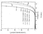
- FIG. 5 shows forward biased current density vs. voltage ( J-V ) characteristics.
- Plots 510, 520, 530 and 540 show the characteristics of bottom OLED 402 (green in stack), top OLED 404 (red in stack), the discrete green-emitting OLED (green control), and the discrete red-emitting OLED (red control), respectively.
- Top OLED 404 exhibits a drive voltage of about 12 V. This drive voltage is significantly lower than the drive voltages between 15 V and 25 V reported for similar OLEDs by Burrows et al., Color-tunable organic light emitting devices , Appl. Phys. Lett. 69 (20), 2959 (1996), which is incorporated by reference.
- the drive voltage for top OLED 404 is only 1 V higher than that of the discrete red-emitting OLED.
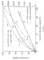
- Figure 6 shows luminescence vs. current density ( L-J ) characteristics.
- Plots 610, 620, 630 and 640 show the characteristics for bottom OLED 402 (green in stack), top OLED 404 (red in stack), the discrete green-emitting OLED (green control), and the discrete red-emitting OLED (red control), respectively.
- the luminance is based on a measurement of the light emitted from the bottom of glass layer 405, i.e ., the side opposite the OLEDs.
- the quantum efficiencies calculated from these measurements are 1% for bottom OLED 402, 0.4% for top OLED 404, in comparison with 0.8% for the discrete green-emitting OLED, and 0.7% for the discrete red-emitting OLED.
- the ratio of luminescence emitted from the top of SOLED 400 to luminescence emitted from the bottom of SOLED 400 was measured as 1:0.067 for OLED 404 and 1:0.51 for OLED 402. Hence, the total external quantum efficiency of top OLED 404 is 1.1%, and that of bottom OLED 402 is 0.6%.
- the red OLEDs i.e. , top OLED 404 and the discrete red-emitting OLED, exhibit a decrease in efficiency at high current densities relative to the green OLEDs, i.e. , bottom OLED 402 and the discrete green-emitting OLED, as shown in Figure 6 by a lower slope in the plots of luminescence v. current density for the red OLEDs at higher current densities. This decrease in efficiency is likely due to slow ( ⁇ 30 ⁇ s) phosphorescent decay, leading to saturation of the PtOEP sites in the emissive region.
- Top OLED 404 exhibits a luminance of 35 cd/m 2 , and a current density of 24 mA/cm 2 at a drive voltage of 12 V. These numbers are sufficient to meet video display standards.
- a microcavity effect may cause the wavelength of light emitted to vary depending on the viewing angle. Emission spectra were measured for OLED 402, OLED 404, the discrete red-emitting OLED, and the discrete green-emitting OLED.
- Figure 7 shows emission spectra of light emitted from OLED 402 and OLED 404.
- Plot 710 green top normal
- Plots 720 green substrate normal
- 730 green substrate 60° off normal
- Plots 720 green substrate normal
- Plots 720 and 730 are plots of spectra emitted from OLED 402 trough the bottom of SOLED 400, in directions normal to the plane of SOLED 400 and 60° off-normal, respectively.
- Plot 740 (red top normal) is a plot of a spectrum emitted from OLED 404 trough the top of SOLED 400 in a direction normal to the plane of SOLED 400.
- Plots 750 red substrate normal
- 760 red substrate 60° off normal
- Plots 720 and 730 are very similar, as are plots 750 and 760, demonstrating that the angular dependencies of the bottom emission spectra are negligible for both OLED 402 and OLED 404.
- SOLEDs similar to SOLED 400 are suitable for applications such as large screen televisions, where the perceived color preferable remains relatively constant as the viewing angle is changed.
- Plot 740 is very similar to plot 750, indicating that top and bottom emission of OLED 404 are about the same. However, plot 710 is shifted about 50 nm. relative to plot 720, indicating that there are some microcavity effects present in SOLED 400.
- Measurements (not shown) corresponding to the measurements shown in Figure 7 were taken for the discrete red-emitting and green-emitting OLEDs.
- the measured emission spectra of each discrete OLED remained relatively constant, regardless of whether the spectra were measured from the top or bottom of the device, and regardless of viewing angle. This lack of change in the emission spectra indicate that any microcavity effects in the discrete OLEDs are weak.
- Curves 715, 725, 735, 745, 755 and 765 are fits to plots 710, 720, 730, 740, 750 and 760, respectively, according to a model of cavity effects disclosed by U.S. Patent Application 08/858,994, filed May 20, 1997, which is incorporated herein by reference.
- This fitting model uses several parameters, including the refractive indices of the organic and electrode layers of SOLED 400, i.e ., layers 410, 415, 420, 425, 430, 435, 440, 445 and 450. Hole injection enhancement layers 415 and 435 were disregarded for purposes of the fitting. Table 2 shows dispersion parameters for the materials used in the fitting.
- the thicknesses of the organic layers were calibrated to an accuracy of 2% during fabrication, and were treated as well defined parameters during the fitting.
- the exciton distributions in the emissive regions were assumed to decay exponentially with distance from the ⁇ -NPD/luminescent layer interface with a characteristic diffusion length of 100 ⁇ .
- the actual thickness of electrode layers 430a 430b, 450a and 450b are somewhat uncertain, because Mg:Ag layers, such as layers 430a and 450a may be oxidized to some extent by the subsequent deposition of an ITO layer, such as layers 430b and 450b. This oxidation can change the thickness as well as the optical properties of layers 430a, 430b, 450a and 450b.
- Curves 715, 725, 735, 745, 755, and 765 were obtained by assuming a thickness of 200 ⁇ for Mg:Ag layers 430a and 450a and a thickness of 780 ⁇ for ITO layers 430b and 450b.
- the discrepancy between the red emission spectra and corresponding fits in the IR spectral region is attributed to the dispersion in hole injection enhancement layer 415, which was not included in the calculation.
- Figure 8 shows two-color tuning spectra, obtained by measuring the emission from the bottom of SOLED 400 in a direction normal to the plane of SOLED 400 while applying different combinations of voltages V G across OLED 402 and V R across OLED 404.
- CIE Commission Internationale de L'Éclairage
- SOLED 400 can be further improved by reducing the thickness of Mg:Ag layers 430a and 450a. Such a reduction in thickness is expected to reduce internal reflections, microcavity effects, and the dependence of perceived color on viewing angle, while increasing transparency.
Landscapes
- Electroluminescent Light Sources (AREA)
- Chemical Vapour Deposition (AREA)
- Other Surface Treatments For Metallic Materials (AREA)
- Chemically Coating (AREA)
- Physical Vapour Deposition (AREA)
Applications Claiming Priority (2)
| Application Number | Priority Date | Filing Date | Title |
|---|---|---|---|
| US15421698A | 1998-09-16 | 1998-09-16 | |
| US154216 | 1998-09-16 |
Publications (1)
| Publication Number | Publication Date |
|---|---|
| EP0987774A2 true EP0987774A2 (fr) | 2000-03-22 |
Family
ID=22550479
Family Applications (1)
| Application Number | Title | Priority Date | Filing Date |
|---|---|---|---|
| EP99104907A Withdrawn EP0987774A2 (fr) | 1998-09-16 | 1999-03-12 | Electrode avec injection des trous améliorée |
Country Status (2)
| Country | Link |
|---|---|
| EP (1) | EP0987774A2 (fr) |
| JP (1) | JP2000091084A (fr) |
Cited By (20)
| Publication number | Priority date | Publication date | Assignee | Title |
|---|---|---|---|---|
| EP1531503A1 (fr) * | 2003-11-12 | 2005-05-18 | Lg Electronics Inc. | Dispositif electroluminescent organique et methode de sa fabrication |
| EP1256989B1 (fr) * | 2001-05-10 | 2007-11-14 | Eastman Kodak Company | Diode organique électroluminescente avec rapport de contraste élevé |
| US7309531B2 (en) | 2001-11-22 | 2007-12-18 | Nippon Soda Co., Ltd. | El device |
| US7514861B2 (en) | 2005-11-24 | 2009-04-07 | Chunghwa Picture Tubes, Ltd. | Organic electro-luminescent device |
| CN100514703C (zh) * | 2005-11-29 | 2009-07-15 | 中华映管股份有限公司 | 有机电致发光元件 |
| CN100517795C (zh) * | 2004-04-21 | 2009-07-22 | 友达光电股份有限公司 | 有机发光二极管及包含其的显示面板与通讯装置 |
| US7888594B2 (en) | 2007-11-20 | 2011-02-15 | Guardian Industries Corp. | Photovoltaic device including front electrode having titanium oxide inclusive layer with high refractive index |
| US7915808B2 (en) | 2000-06-05 | 2011-03-29 | Semiconductor Energy Laboratory Co., Ltd. | Light emitting device including EL elements for emitting lights of different colors |
| CN102024912A (zh) * | 2010-09-30 | 2011-04-20 | 友达光电股份有限公司 | 电致发光装置的发光单元及其制造方法 |
| US7964788B2 (en) | 2006-11-02 | 2011-06-21 | Guardian Industries Corp. | Front electrode for use in photovoltaic device and method of making same |
| US8012317B2 (en) | 2006-11-02 | 2011-09-06 | Guardian Industries Corp. | Front electrode including transparent conductive coating on patterned glass substrate for use in photovoltaic device and method of making same |
| US8022291B2 (en) | 2008-10-15 | 2011-09-20 | Guardian Industries Corp. | Method of making front electrode of photovoltaic device having etched surface and corresponding photovoltaic device |
| US8049418B2 (en) | 2000-08-28 | 2011-11-01 | Semiconductor Energy Laboratory Co., Ltd. | Light emitting device comprising triplet compound in electroluminescent layer |
| US8076571B2 (en) * | 2006-11-02 | 2011-12-13 | Guardian Industries Corp. | Front electrode for use in photovoltaic device and method of making same |
| US8203073B2 (en) | 2006-11-02 | 2012-06-19 | Guardian Industries Corp. | Front electrode for use in photovoltaic device and method of making same |
| US8334452B2 (en) | 2007-01-08 | 2012-12-18 | Guardian Industries Corp. | Zinc oxide based front electrode doped with yttrium for use in photovoltaic device or the like |
| US8390188B2 (en) | 2010-09-20 | 2013-03-05 | Au Optronics Corporation | Light emitting unit of electroluminescence device capable of increasing aperture rate manufacturing method thereof |
| US8502066B2 (en) | 2009-11-05 | 2013-08-06 | Guardian Industries Corp. | High haze transparent contact including insertion layer for solar cells, and/or method of making the same |
| US9209326B2 (en) * | 2008-02-04 | 2015-12-08 | Lg Electronics Inc. | Solar cell having multiple transparent conductive layers and manufacturing method thereof |
| CN106684072A (zh) * | 2017-03-02 | 2017-05-17 | 江苏集萃有机光电技术研究所有限公司 | 一种oled装置 |
Families Citing this family (8)
| Publication number | Priority date | Publication date | Assignee | Title |
|---|---|---|---|---|
| JP2002151269A (ja) * | 2000-08-28 | 2002-05-24 | Semiconductor Energy Lab Co Ltd | 発光装置 |
| US6737177B2 (en) * | 2001-11-08 | 2004-05-18 | Xerox Corporation | Red organic light emitting devices |
| JP2003282276A (ja) * | 2002-03-26 | 2003-10-03 | Morio Taniguchi | 光源装置 |
| JP2003347063A (ja) * | 2002-05-23 | 2003-12-05 | Toshiba Corp | 有機エレクトロルミネッセンス表示素子およびその製造方法 |
| WO2003101158A1 (fr) * | 2002-05-29 | 2003-12-04 | Asahi Glass Company, Limited | Substrat comprenant un film conducteur transparent et dispositif electroluminescent organique |
| WO2004108857A1 (fr) * | 2003-06-02 | 2004-12-16 | Fuji Photo Film Co., Ltd. | Dispositifs electroluminescents organiques et composes de complexes metalliques |
| CN100565968C (zh) * | 2005-06-03 | 2009-12-02 | 皇家飞利浦电子股份有限公司 | 有机电致发光光源 |
| JP2007234259A (ja) * | 2006-02-27 | 2007-09-13 | Hitachi Displays Ltd | 有機el表示装置 |
-
1999
- 1999-03-08 JP JP11060091A patent/JP2000091084A/ja active Pending
- 1999-03-12 EP EP99104907A patent/EP0987774A2/fr not_active Withdrawn
Cited By (33)
| Publication number | Priority date | Publication date | Assignee | Title |
|---|---|---|---|---|
| US8304985B2 (en) | 2000-06-05 | 2012-11-06 | Semiconductor Energy Laboratory Co., Ltd. | Light emitting device having singlet and triplet compounds with different emission colors |
| US10777615B2 (en) | 2000-06-05 | 2020-09-15 | Semiconductor Energy Laboratory Co., Ltd. | Light-emitting device |
| US10446615B2 (en) | 2000-06-05 | 2019-10-15 | Semiconductor Energy Laboratory Co., Ltd. | Light-emitting device |
| US10192934B2 (en) | 2000-06-05 | 2019-01-29 | Semiconductor Energy Laboratory Co., Ltd. | Light-emitting device having light emission by a singlet exciton and a triplet exciton |
| US9917141B2 (en) | 2000-06-05 | 2018-03-13 | Semiconductor Energy Laboratory Co., Ltd. | Light-emitting device having singlet and triplet compounds |
| US9564472B2 (en) | 2000-06-05 | 2017-02-07 | Semiconductor Energy Laboratory Co., Ltd. | Light-emitting device |
| US9362343B2 (en) | 2000-06-05 | 2016-06-07 | Semiconductor Energy Laboratory Co., Ltd. | Iridium-containing active-matrix EL display module |
| US7915808B2 (en) | 2000-06-05 | 2011-03-29 | Semiconductor Energy Laboratory Co., Ltd. | Light emitting device including EL elements for emitting lights of different colors |
| US8907559B2 (en) | 2000-06-05 | 2014-12-09 | Semiconductor Energy Laboratory Co., Ltd. | Semiconductor device having display portion with plural pixels |
| US8674599B2 (en) | 2000-06-05 | 2014-03-18 | Semiconductor Energy Laboratory Co., Ltd. | Light emitting device having fluorescence and phosphoresence compound |
| US8975813B2 (en) | 2000-08-28 | 2015-03-10 | Semiconductor Energy Laboratory Co., Ltd. | Light emitting device |
| US8415876B2 (en) | 2000-08-28 | 2013-04-09 | Semiconductor Energy Laboratory Co., Ltd. | Light emitting device and display comprising light emitting device |
| US8049418B2 (en) | 2000-08-28 | 2011-11-01 | Semiconductor Energy Laboratory Co., Ltd. | Light emitting device comprising triplet compound in electroluminescent layer |
| EP1256989B1 (fr) * | 2001-05-10 | 2007-11-14 | Eastman Kodak Company | Diode organique électroluminescente avec rapport de contraste élevé |
| US7309531B2 (en) | 2001-11-22 | 2007-12-18 | Nippon Soda Co., Ltd. | El device |
| EP1531503A1 (fr) * | 2003-11-12 | 2005-05-18 | Lg Electronics Inc. | Dispositif electroluminescent organique et methode de sa fabrication |
| CN100517795C (zh) * | 2004-04-21 | 2009-07-22 | 友达光电股份有限公司 | 有机发光二极管及包含其的显示面板与通讯装置 |
| US7514861B2 (en) | 2005-11-24 | 2009-04-07 | Chunghwa Picture Tubes, Ltd. | Organic electro-luminescent device |
| CN100514703C (zh) * | 2005-11-29 | 2009-07-15 | 中华映管股份有限公司 | 有机电致发光元件 |
| US7964788B2 (en) | 2006-11-02 | 2011-06-21 | Guardian Industries Corp. | Front electrode for use in photovoltaic device and method of making same |
| US8012317B2 (en) | 2006-11-02 | 2011-09-06 | Guardian Industries Corp. | Front electrode including transparent conductive coating on patterned glass substrate for use in photovoltaic device and method of making same |
| US8076571B2 (en) * | 2006-11-02 | 2011-12-13 | Guardian Industries Corp. | Front electrode for use in photovoltaic device and method of making same |
| US8203073B2 (en) | 2006-11-02 | 2012-06-19 | Guardian Industries Corp. | Front electrode for use in photovoltaic device and method of making same |
| US8936842B2 (en) | 2007-01-08 | 2015-01-20 | Guardian Industris Corp. | Low-E coating having zinc aluminum oxide based layer doped with yttrium |
| US8334452B2 (en) | 2007-01-08 | 2012-12-18 | Guardian Industries Corp. | Zinc oxide based front electrode doped with yttrium for use in photovoltaic device or the like |
| US7888594B2 (en) | 2007-11-20 | 2011-02-15 | Guardian Industries Corp. | Photovoltaic device including front electrode having titanium oxide inclusive layer with high refractive index |
| US9209326B2 (en) * | 2008-02-04 | 2015-12-08 | Lg Electronics Inc. | Solar cell having multiple transparent conductive layers and manufacturing method thereof |
| US8022291B2 (en) | 2008-10-15 | 2011-09-20 | Guardian Industries Corp. | Method of making front electrode of photovoltaic device having etched surface and corresponding photovoltaic device |
| US8502066B2 (en) | 2009-11-05 | 2013-08-06 | Guardian Industries Corp. | High haze transparent contact including insertion layer for solar cells, and/or method of making the same |
| US8390188B2 (en) | 2010-09-20 | 2013-03-05 | Au Optronics Corporation | Light emitting unit of electroluminescence device capable of increasing aperture rate manufacturing method thereof |
| CN102024912B (zh) * | 2010-09-30 | 2012-10-24 | 友达光电股份有限公司 | 电致发光装置的发光单元及其制造方法 |
| CN102024912A (zh) * | 2010-09-30 | 2011-04-20 | 友达光电股份有限公司 | 电致发光装置的发光单元及其制造方法 |
| CN106684072A (zh) * | 2017-03-02 | 2017-05-17 | 江苏集萃有机光电技术研究所有限公司 | 一种oled装置 |
Also Published As
| Publication number | Publication date |
|---|---|
| JP2000091084A (ja) | 2000-03-31 |
Similar Documents
| Publication | Publication Date | Title |
|---|---|---|
| Gu et al. | A metal-free, full-color stacked organic light-emitting device | |
| Gu et al. | High-efficiency, low-drive-voltage, semitransparent stacked organic light-emitting device | |
| US6551725B2 (en) | Inorganic buffer structure for organic light-emitting diode devices | |
| US6188176B1 (en) | Organic electroluminescent device and preparation method with ITO electrode (111) orientation | |
| US5981306A (en) | Method for depositing indium tin oxide layers in organic light emitting devices | |
| US5922396A (en) | Electron transporting and light emitting layers based on organic free radicals | |
| JP4142782B2 (ja) | 有機el素子 | |
| JP2000091084A (ja) | ホ―ル注入性改良電極 | |
| US7141924B2 (en) | Multi-layer cathode in organic light-emitting devices | |
| JP3428152B2 (ja) | 有機el素子の製造方法 | |
| JP2006059818A (ja) | 有機装置のための透明コンタクト | |
| JPH08102360A (ja) | 有機無機複合薄膜型電界発光素子 | |
| US20030129447A1 (en) | Sputtered cathode having a heavy alkaline metal halide-in an organic light-emitting device structure | |
| US20050073245A1 (en) | White electrophosphorescence from semiconducting polymer blends | |
| JP4543446B2 (ja) | 有機el素子 | |
| KR100338251B1 (ko) | 유기발광전계소자 | |
| JP2000252074A (ja) | 有機el素子 | |
| US6597109B1 (en) | Organic EL device and method for production thereof | |
| JP4247016B2 (ja) | 有機el表示装置 | |
| US20030224204A1 (en) | Sputtered cathode for an organic light-emitting device having an alkali metal compound in the device structure | |
| CN100469201C (zh) | 显示装置及其制造方法 | |
| US6917158B2 (en) | High-qualty aluminum-doped zinc oxide layer as transparent conductive electrode for organic light-emitting devices | |
| US7687990B2 (en) | OLED device with short reduction | |
| JP2000012226A (ja) | 有機電界発光素子 | |
| JP2000012225A (ja) | 有機電界発光素子 |
Legal Events
| Date | Code | Title | Description |
|---|---|---|---|
| PUAI | Public reference made under article 153(3) epc to a published international application that has entered the european phase |
Free format text: ORIGINAL CODE: 0009012 |
|
| AK | Designated contracting states |
Kind code of ref document: A2 Designated state(s): AT BE CH CY DE DK ES FI FR GB GR IE IT LI LU MC NL PT SE |
|
| AX | Request for extension of the european patent |
Free format text: AL;LT;LV;MK;RO;SI |
|
| STAA | Information on the status of an ep patent application or granted ep patent |
Free format text: STATUS: THE APPLICATION HAS BEEN WITHDRAWN |
|
| 18W | Application withdrawn |
Withdrawal date: 20020516 |