EP0988699B1 - Betriebsmittelteilung in einem digitalen filter - Google Patents
Betriebsmittelteilung in einem digitalen filter Download PDFInfo
- Publication number
- EP0988699B1 EP0988699B1 EP99902725A EP99902725A EP0988699B1 EP 0988699 B1 EP0988699 B1 EP 0988699B1 EP 99902725 A EP99902725 A EP 99902725A EP 99902725 A EP99902725 A EP 99902725A EP 0988699 B1 EP0988699 B1 EP 0988699B1
- Authority
- EP
- European Patent Office
- Prior art keywords
- data
- output
- coefficient
- registers
- values
- Prior art date
- Legal status (The legal status is an assumption and is not a legal conclusion. Google has not performed a legal analysis and makes no representation as to the accuracy of the status listed.)
- Expired - Lifetime
Links
- 238000005070 sampling Methods 0.000 claims description 26
- 238000000034 method Methods 0.000 claims description 19
- 230000008569 process Effects 0.000 claims description 10
- 230000004087 circulation Effects 0.000 description 20
- 230000003044 adaptive effect Effects 0.000 description 9
- 230000004044 response Effects 0.000 description 8
- 230000006978 adaptation Effects 0.000 description 4
- 238000010586 diagram Methods 0.000 description 3
- 230000009467 reduction Effects 0.000 description 3
- 230000005540 biological transmission Effects 0.000 description 2
- 238000012986 modification Methods 0.000 description 2
- 230000004048 modification Effects 0.000 description 2
- 238000009825 accumulation Methods 0.000 description 1
- 230000002411 adverse Effects 0.000 description 1
- 238000004364 calculation method Methods 0.000 description 1
- 230000003247 decreasing effect Effects 0.000 description 1
- 230000007812 deficiency Effects 0.000 description 1
- 230000001419 dependent effect Effects 0.000 description 1
- 230000000694 effects Effects 0.000 description 1
- 238000001914 filtration Methods 0.000 description 1
Images


Classifications
-
- H—ELECTRICITY
- H03—ELECTRONIC CIRCUITRY
- H03H—IMPEDANCE NETWORKS, e.g. RESONANT CIRCUITS; RESONATORS
- H03H17/00—Networks using digital techniques
- H03H17/02—Frequency selective networks
- H03H17/0294—Variable filters; Programmable filters
-
- H—ELECTRICITY
- H03—ELECTRONIC CIRCUITRY
- H03H—IMPEDANCE NETWORKS, e.g. RESONANT CIRCUITS; RESONATORS
- H03H17/00—Networks using digital techniques
- H03H17/02—Frequency selective networks
- H03H17/0223—Computation saving measures; Accelerating measures
- H03H17/0225—Measures concerning the multipliers
-
- H—ELECTRICITY
- H03—ELECTRONIC CIRCUITRY
- H03H—IMPEDANCE NETWORKS, e.g. RESONANT CIRCUITS; RESONATORS
- H03H17/00—Networks using digital techniques
- H03H17/02—Frequency selective networks
- H03H17/0283—Filters characterised by the filter structure
- H03H17/0292—Time multiplexed filters; Time sharing filters
-
- H—ELECTRICITY
- H03—ELECTRONIC CIRCUITRY
- H03H—IMPEDANCE NETWORKS, e.g. RESONANT CIRCUITS; RESONATORS
- H03H2218/00—Indexing scheme relating to details of digital filters
- H03H2218/08—Resource sharing
- H03H2218/085—Multipliers
Definitions
- the present invention is directed to resource sharing in a digital filter.
- the invention is directed to a digital filter comprised of cells which process plural data values and filter coefficients using the same circuitry.
- FIR filters such as finite impulse response (hereinafter "FIR") filters
- Each filter cell includes a data register for storing a sampled data value and a coefficient register which stores a coefficient for that particular cell.
- FIR finite impulse response
- Each filter cell includes a data register for storing a sampled data value and a coefficient register which stores a coefficient for that particular cell.
- the same sampled data value is input sequentially to each filter cell, and is multiplied by a coefficient for that cell.
- the results of these multiplications are then output and combined in order to generate the filter's output.
- filter outputs require a different number of filter cells. For example, only two filter cells may be required to simulate the effects of a simple lowpass filter. Additional filter cells, however, may be required to perform more complex filtering. In this regard, generally speaking, as the complexity of the filter's function increases, the number of cells in the filter increases, thereby leading to an increase in the filter's size. This can be problematic, particularly in cases where a large number of filter cells are required, but where there is a limited amount of available space.
- two multiplexers are used to control which data values and which coefficients are transmitted to the multiplication circuit.
- These multiplexers introduce a propagation delay into the filter cell which reduces the maximum clock frequency at which the filter can operate.
- the multiplexers take up additional space, thereby reducing the space savings achieved by the reduction in the number of multiplication circuits.
- an adaptive digital filter includes adaptation circuitry in each tap cell, which is designed to update each tap cell's coefficients based on a variety of factors, such as channel characteristics, etc., that could affect data transmission.
- the adaptation circuitry enhances the filter's functionality, the adaptation circuitry also increases the size of the filter.
- US-A-5479363 discloses a programmable digital signal processor using switchable unit-delays for hardware allocation.
- a switchable unit-delay has been developed for implementation of programmable digital finite impulse response filters and correlators.
- a p-tap consisting of this switchable unit-delay and a two-non-zero-digit partial product generator and adder have been implemented.
- the combination of several p-taps, made possible by the switchable unit-delay allows for implementation of coefficients with more than two non-zero digits.
- the switchable unit-delay not only allows the programing of the number of taps and the specific tap-coefficient values, it provides the capability for programing the allocation of hardware resources to each filter tap.
- GB-A-2161345 discloses an adaptive filter with a tapped delay line that has a two-dimensional storage array arranged in rows and columns to store weighting factors for individual contributions. All weighting factors in parallel are read out and written into the array bit-serially during coefficient-update processing, and are serially read out and written into the array bit-parallel during tap contribution multiplications and accumulation.
- the filter is implemented as a large scale integrated circuit and finds applications, for example, in echo cancellation and decision feedback equalization.
- the present invention addresses the foregoing need by providing a way in which to share circuitry for coefficient adaptation and multiplication within a single filter cell of a digital filter.
- a plurality of coefficient registers in the filter cell circulate values corresponding to the coefficients, while one or more data registers in the filter cell circulate a data value such that the data value is output each time a different one of the coefficients is output.
- a circuit, such as a multiplication circuit, within the cell then processes output data values and coefficients.
- the present invention is a digital filter as defined in claim 1.
- a preferred embodiment of the invention is defined by claim 2.
- This feature of the invention facilitates input of data into the system so that the resources of the filter cell may be shared by additional data values.
- a particularly preferred embodiment of the invention is defined by claim 6.
- the present invention provides a method of generating processed data in a digital filter cell as defined by claim 11.
- This method reduces the amount of circuitry required in a filter cell by including, in a single filter cell, both circuitry for adapting filter coefficients and circuitry used to process those coefficients.
- this method it is possible to reduce the number of filter cells required in the filter, thereby also reducing the overall size of the filter.
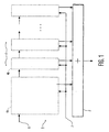
- FIG. 1 shows an adaptive FIR filter having filter cells which implement resource sharing in accordance with the present invention.
- digital filter 1 includes adder circuit 2 and a plurality of filter cells 4 (4a, 4b,.). Any number of these filter cells 4 may be included in digital filter 1, depending upon the desired functionality of the filter.
- Digital filter 1 operates by sampling data from a signal at a predetermined sampling rate, and sequentially shifting the sampled data, labeled 6 in Figure 1, into each of filter cells 4 in accordance with a sampling clock signal. For example, sampled data 6 is shifted into filter cell 4a in response to a first sampling clock pulse. Next, when additional data is sampled at a next sampling clock pulse, that additional data is shifted into filter cell 4a, and the data already in filter cell 4a is shifted into filter cell 4b, and so on.
- Each of filter cells 4 processes the sampled data within a single period of the sampling clock signal. This processing may take into account external input 7, which is shown in Figure 1 and of which examples are described in detail below. After sampled data has been processed by a filter cell, resulting processed data is output to adder circuit 2. Adder circuit 2 combines the output data from each of filter cells 4 in order to generate the output of filter 1.
- FIG. 2 shows the internal circuitry of filter cell 4a shown in Figure 1. Since filter cells 4 are identical in structure, for the sake of brevity, only filter cell 4a will be described herein.
- filter cell 4a includes input register 9, multiplexer 10, data registers 11, processing circuit 12, which is preferably a multiplier circuit, coefficient registers 14 (14a, 14b, 14c, 14d), and logic stages 15, 16, 17 and 18.
- processing circuit 12 which is preferably a multiplier circuit
- coefficient registers 14 14a, 14b, 14c, 14d
- the arrangement shown in Figure 2 enables data values shifted into filter cell 4a to share both processing circuit 12 and coefficients output by coefficient registers 14, as is clear from the following description.
- input register 9 is arranged in series with multiplexer 10 and data registers 11 (11a, 11b, 11c). Both input register 9 and data registers 11 can comprise conventional shift registers, which shift data in response to a clock signal. In this regard, as described in more detail below, input register 9 shifts data in response to the sampling clock signal noted above. In contrast, data registers 11 shift data in response to a circulation clock signal, which has a frequency that is a multiple of the frequency of the sampling clock signal. This arrangement provides for multiple shifting of each of data registers 11 for every single shift of input register 9.
- Data register 11a outputs a data value to processing circuit 12 at each circulation clock pulse. As shown in Figure 2, that same data value is fed back to multiplexer 10 via feedback path 20. Multiplexer 10 also receives selection signal 21 and an output from input register 9. Selection signal 21 causes multiplexer 10 to shift data from register 9 during sampling clock pulses, and causes multiplexer 10 to shift data from feedback path 20 during circulation clock pulses. By virtue of this arrangement, during circulation clock pulses, data values circulate within data registers 11. However, at each sampling clock pulse, an additional data value from input register 9 is shifted into data registers 11, where the additional data value is circulated.
- data registers 11 circulate a first set of data values for a predetermined time, and, following the predetermined time, data registers 11 circulate a second set of data values (which includes the additional data value) for the predetermined time, and so on.
- data registers 11 are designed to circulate the same number of data values. Accordingly, each time an additional data value is input into data registers 11, one of the data values already within data registers 11 is removed. Specifically, the data value in feedback path 20 (i.e., the data value which was last output to processing circuit 12) is removed, since that data value is not input back into data registers 11. Since only one data value is removed per sampling clock period, data registers 11 generally circulate a data value for a plurality of sampling clock periods before that data value is removed. The exception to this general rule is the case in which a single data value is circulated in a single data register. In this case, the data value only needs to be circulated for one sampling clock period for reasons which will become clear below. An example of a filter cell having only one data register is provided in the second embodiment below.
- Coefficient registers 14 are arranged to circulate a plurality of coefficient values that correspond to a plurality of coefficients, so that each of the plurality of coefficient values is output once during a predetermined period. More specifically, coefficient values are shifted among coefficient registers 14 such that, at a predetermined period, which preferably corresponds to a period of the circulation clock signal, coefficient register 14a outputs a coefficient to processing circuit 12.
- processing circuit 12 receives a data value from data register 11a and a coefficient from coefficient register 14a.
- processing circuit 12 processes (e.g., multiplies) these two values to generate an output for the filter cell.
- processing circuit 12 can comprise any type of circuit depending, of course, upon the type of filter cell in which the invention is implemented and the type of coefficients being shared.
- coefficient registers 14 circulate coefficient values by feeding a coefficient output to processing circuit 12 back along feedback path 22.
- This arrangement permits the same coefficients to circulate among coefficient registers 14, thereby making it possible for those coefficients to be shared by data values in data registers 11. That is, as described above, data registers 11 circulate a data value for a plurality of sampling clock periods before that data value is removed. As a result, the same data value is output several times to processing circuit 12 over several sampling clock signal periods. Each time that the same data value is output to processing circuit 12, a different coefficient value is output thereto from coefficient register 14a. As a result, each data value is processed with each coefficient. This process is illustrated below with respect to Figures 2 and 3.
- filter cell 4a is an adaptive filter cell, meaning that coefficients therein may be updated periodically to correct unwanted changes in the data values caused, e.g., by changes in the transmission channel or the like.
- these updates are made via logic stages 15 to 18, where external inputs 25 to 28 can comprise filter error (i.e., a difference between expected and actual filter outputs) or the like.
- coefficient computation is "broken up" into separate pipe-line stages, each of which is performed between appropriate coefficient registers.
- coefficient values in coefficient registers 14b, 14c and 14d do not necessarily comprise actual coefficients, hence the "prime” indications on C2, C3 and C4. Rather, the coefficient values in these coefficient registers may represent intermediate values of the computation of the actual coefficients. This feature of the invention is advantageous, since it allows coefficient circulating and updating to be performed simultaneously, thereby further reducing the amount of hardware required to implement filter cell 4a.
- logic stages 15 to 18 update the coefficients using the well-known LMS algorithm.
- the invention is not limited to updating the coefficients using this algorithm, and that any such algorithm may be used.
- Figure 3 shows a timing table which is used to explain the operation of digital filter cell 4a from times T0 to T13 for data values of 1 to 8 and coefficient values of 1 to 4. More specifically, as shown in Figure 3, at time T0, coefficients values of 1, 2, 3 and 4 are in coefficient registers 14a, 14b, 14c and 14d, respectively, while data values of 1, 2 and 3 are in data registers 11a, 11b and 11c, respectively, and a data value of 4 is in input register 9.
- the following traces the path of data value 4 through filter cell 4a in order to illustrate sharing of both processing circuit 12 and coefficient values 1, 2, 3 and 4. It is to be understood, however, that the following description relating to data value 4 applies equally to all data values (e.g., data values 1, 2, 3, 5, 6...) input into filter cell 4a.
- coefficient values of 1 to 4 are being circulated in coefficient registers 14 in accordance with the circulation clock signal. That is, as shown in Figure 3, at time T1 coefficient value 2 is at coefficient register 14a, at time T2 coefficient value 3 is at coefficient register 14a, and at time T3 coefficient value 4 is at coefficient register 14a. Thus, at time T3 (i.e., at the same time that data value 4 is output from data register 11a), coefficient value 4 is output to processing circuit 12, where coefficient value 4 is processed with data value 4.
- selection signal 21 indicates to multiplexer 10 that a sampling clock pulse has been received.
- data value 5 is shifted into data register 11c from input register 9, while, at the same time, data value 2 is removed from data registers 11. That is, at this point, data value 2 is input to multiplexer 10, which selects data value 5 and not data value 2 for shifting into data register 11c.
- the circulation times for data values 3, 4 and 5 are shown by bracket 32 in Figure 3. Circulation of data values 3, 4 and 5 continue in the manner described above concurrently with circulation of coefficient values 1, 2, 3 and 4 in coefficient registers 14. As a result of these circulations, at time T6, data value 4 is output to processing circuit 12 and coefficient value 3 is also output to processing circuit 12.
- filter cell 4a processes data value 4 with each of coefficients 1, 2, 3 and 4. This is highlighted by the circled values of Figure 3.
- filter cell 4a does this using the same processing circuit. Accordingly, the invention accomplishes sharing of both coefficient values and processing circuit 12 within a single filter cell.
- the invention is not limited to using four data values and four coefficients in the manner set forth above. Rather, any number of coefficients and data values may be used in a filter cell so long as data registers in the filter cell circulate a data value for a time which is at least as long as the period during which the coefficients are circulated so that the data value is output each time that a different coefficient is output. Moreover, it is also noted that the invention need not be implemented using logic stages interspersed among coefficient registers.
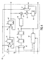
- Figure 4 shows an example of a two coefficient, one data register filter, in which different logic stages are not interspersed among coefficient registers.
- the embodiment of the invention shown in Figure 4, namely filter cell 40 includes input register 41, data register 42, multiplexers 44, 45, 46 and 47, storage register 48, round-off/truncation circuit 49, multiplier circuit 50, adder circuit 51, coefficient update (combinatorial) circuit 52, and coefficient registers 53 and 54.
- operation of filter cell 40 is essentially the same as filter cell 4a shown in Figure 2. Accordingly, focus here will be on operational aspects of filter cell 40 which differ from those of filter cell 4a above.
- Filter cell 40 includes storage register 48, which was not included in filter cell 4a above.
- Storage register 48 stores the product of a data value and each coefficient.
- multiplexer 47 provides these values to adder circuit 51, which adds these values together and outputs the sum of these products from filter cell 40.
- Round-off/truncation circuit 49 is also provided to round-off/truncate updated coefficient values prior to their multiplication with a data value.
- Coefficient update circuit 52 is used to update coefficient values based, for example, on external information such as filter error (i.e., the difference between expected and actual filter outputs), data from previous or following filter cells, etc.
- Multiplexer 46 which is controlled by read/write taps signal 56, also provides filter cell 40 with the ability to read coefficients from, and write coefficients to, a filter cell.
- filter cell 40 circulates coefficients in coefficient registers 53 and 54, and circulates a data value in data register 42. This circulation is identical to that described above, except that coefficient update circuit 52 updates values of the coefficients, rather than interspersed logic stages. Likewise, shifting of additional data to and from input register 41 is identical to that described above. Accordingly, for the sake of brevity, a detailed description of these processes is omitted here.
Landscapes
- Engineering & Computer Science (AREA)
- Physics & Mathematics (AREA)
- Computer Hardware Design (AREA)
- Mathematical Physics (AREA)
- Computing Systems (AREA)
- Theoretical Computer Science (AREA)
- Complex Calculations (AREA)
Claims (15)
- Digitales Filter (1) mit einer Filterzelle (4a) zum Erzeugen verarbeiteter Daten, dadurch gekennzeichnet, dass die Filterzelle die nachfolgenden Elemente umfasst:eine Anzahl Koeffizientenregister (14), die dazu vorgesehen sind, eine Anzahl Koeffizientenwerte in Umlauf zu bringen, die einer Anzahl Koeffizienten entsprechen, so dass jeder der vielen Koeffizienten während einer vorbestimmten Periode einmal ausgegeben wird;ein oder mehrere Datenregister (11), die dazu vorgesehen sind, einen Datenwert in Umlauf zu bringen, und zwar während einer Zeit, die wenigstens ebenso lang ist wie die vorbestimmte Periode, so dass der Datenwert jeweils ausgegeben wird, wenn ein anderer Koeffizient der vielen Koeffizienten ausgeliefert wird; undeine Verarbeitungsschaltung (12), die jeden Ausgangsdatenwert und jeden Ausgangskoeffizienten empfängt und verarbeitete Daten erzeugt, indem jeder Ausgangsdatenwert mit jedem Ausgangskoeffizienten verarbeitet wird.
- Digitales Filter (1) nach Anspruch 1, wobei dieses Filter weiterhin eine Anzahl logischer Stufen (15, 16, 17, 18) aufweist, die unter den vielen Koeffizientenregistem (14) vorgesehen sind um eine Verarbeitung an den Koeffizientenwerten durchzuführen um jeden Koeffizienten der vielen Koeffizienten zu erzeugen, die von den vielen Koeffizientenregistem ausgeliefert werden.
- Digitales Filter (1) nach Anspruch 2, wobei die logischen Stufen eine Verarbeitung durchführen, welche die Koeffizientenwerte entsprechend einer Änderung in einem Datenwert aktualisiert.
- Digitales Filter (1) nach Anspruch 2, wobei die logischen Stufen einen mittleren quadratischen Algorithmus an den Koeffizientenwerten durchführen um jeden der vielen Koeffizienten zu aktualisieren.
- Digitales Filter (1) nach Anspruch 1, das weiterhin ein Eingangsdatenregister (9) aufweist, vorgesehen in Reihe mit dem einen oder mit mehreren Datenregistern (11), das einen zusätzlichen Datenwert von einer Quelle außerhalb der Filterzelle (4a) empfängt;
wobei während der vorbestimmten Periode das Eingangsdatenregister (9), den zusätzlichen Datenwert in das eine oder in die vielen Datenregister (11) schiebt, so dass das eine oder die vielen Datenregister (11) den zusätzlichen Datenwert umlaufen lassen. - Digitales Filter (1) nach Anspruch 5, wobei das eine oder die vielen Datenregister (11) eine Anzahl Datenregister aufweist bzw. aufweisen, die eine Anzahl Datenwerte umlaufen lassen; und wobei die vielen Datenregister (11) einen ersten Satz von Datenwerten eine Zeit lang umlaufen lassen, wobei diese Zeit der vorbestimmten Periode entspricht, und wobei nach dieser vorbestimmten Periode die Anzahl Datenregister (11) einen zweiten Satz von Datenwerten umlaufen lassen, und zwar während einer Zeit, die der vorbestimmten Periode entspricht, wobei der zweite Satz mit Datenwerten den zusätzlichen Datenwert von dem Eingangsdatenregister (9) enthält und die gleiche Anzahl Datenwerte hat wie der erste Satz mit Datenwerten.
- Digitales Filter (1) nach Anspruch 5, wobei dieses Filter weiterhin einen Multiplexer (10) aufweist, der zwischen dem Eingangsdatenregister (9) und dem einen oder den vielen Datenregistern (11) vorgesehen ist, wobei dieser Multiplexer (10) dazu verwendet wird, zu bestimmen, ob der zusätzliche Datenwert in das eine oder in die vielen Datenregister (11) geschoben werden soll, und zwar auf Basis eines Signals, das der vorbestimmten Periode entspricht.
- Digitales Filter nach Anspruch 5, wobei die vorbestimmte Periode einer Abtastperiode des digitalen Filters (1) entspricht.
- Digitales Filter (1) nach Anspruch 1, wobei die Verarbeitungsschaltung (12) eine Multiplizierschaltung aufweist, die jeden Ausgangsdatenwert mit jedem Ausgangskoeffizienten multipliziert, damit ein Ausgangsprodukt erzeugt wird.
- Digitales Filter (1) nach Anspruch 1, wobei dieses Filter die nachfolgenden Elemente umfasst:wobei in jede4r der vielen Filterzellen (4, 40) die Verarbeitungsschaltung Folgendes umfasst:eine Anzahl der genannten Filterzellen (4, 40) wobei jede der Filterzellen dazu vorgesehen ist, eine Anzahl Datenwerte zusammen mit einer Anzahl Koeffizientenwerte zu verarbeiten um einen Filterzellenausgangswert zu erzeugen; undeine Addierschaltung (2), die den Filterzellenausgangswert von jeder Filterzelle (4) addiert, damit ein Filterausgangswert erzeugt wird;eine Multiplizierschaltung (50), die jeden Ausgangsdatenwert und jeden Ausgangskoeffizienten empfängt und ein Ausgangsprodukt erzeugt;ein Speicherregister (48), welches das Ausgangsprodukt jedes Ausgangsdatenwertes und jedes Ausgangskoeffizienten speichert; undeine Addierschaltung (51), welche die Produktwerte addiert, die in dem Speicherregister (48) gespeichert sind, damit ein Filterzellenausgangswert für die Filterzelle (40) erzeugt wird.
- Verfahren zum Erzeugen verarbeiteter Daten in einer digitalen Filterzelle (4a), dadurch gekennzeichnet, dass das Verfahren die nachfolgenden Verfahrensschritte umfasst:unddas Umlaufen lassen einer Anzahl Koeffizientenwerte in vielen Koeffizientenregistern (14) in der digitalen Filterzelle;das Ausliefern jedes der vielen Koeffizienten aus den vielen Koeffizientenregistern (14), und zwar einmal während einer vorbestimmten Periode, wobei die vielen Koeffizienten auf den vielen Koeffizientenwerten basieren;das Umlaufen lassen eines Datenwertes in einem oder in mehreren Datenregistern (11), und zwar während einer Zeit, die wenigstens ebenso lang ist wie die vorbestimmte Periode, wobei der Datenwert von dem einen oder von den vielen Datenregistern (11) ausgeliefert wird, und zwar jeweils, wenn ein anderer Koeffizient der vielen Koeffizienten ausgeliefert wird;das Verarbeiten (12) jedes Ausgangsdatenwertes und jedes Ausgangskoeffizienten um einen verarbeiteten Datenwert zu erzeugen.
- Verfahren nach Anspruch 11, wobei dieses Verfahren weiterhin vor dem Auslieferungsschritt den Verarbeitungsschritt umfasst, und zwar zum Verarbeiten jedes der vielen Koeffizientenwerte zum Erzeugen jedes der vielen Koeffizienten.
- Verfahren nach Anspruch 11, weiterhin mit den nachfolgenden Verfahrensschritten:dem Empfang, in einem Eingangsdatenregister, eines zusätzlichen Datenwertes von einer Quelle außerhalb der Filterzelle (4a); unddem Einschub des zusätzlichen Datenwertes in das eine oder in die vielen Datenregister (11) während der vorbestimmten Periode, so dass das eine oder die vielen Datenregister (11) den zusätzlichen Datenwert umlaufen lassen.
- Verfahren nach Anspruch 13, wobei der Schiebeschritt eine Anzahl Datenwerte in vielen Datenregistern (11) umlaufen lässt; und
wobei ein erster Satz von Datenwerten eine Zeit lang in Umlauf gesetzt wird, und zwar entsprechend der vorbestimmten Periode, und wobei nach der vorbestimmten Periode ein zweiter Satz von Datenwerten eine Zeit lang in Umlauf gesetzt wird, und zwar entsprechend der vorbestimmten Periode, wobei der zweite Satz von Datenwerten den zusätzlichen Datenwert aus dem Eingangsdatenregister (9) aufweist und dieselbe Anzahl Datenwerte hat wie der erste Satz mit Datenwerte. - Verfahren nach Anspruch 13, wobei dieses Verfahren weiterhin den Schritt der Bestimmung umfasst, ob der zusätzliche Datenwert in das eine oder in die vielen Datenregister (11) geschoben werden soll, und zwar auf Basis eines Taktsignals, das der vorbestimmten Periode entspricht.
Applications Claiming Priority (3)
| Application Number | Priority Date | Filing Date | Title |
|---|---|---|---|
| US09/031,698 US6108681A (en) | 1998-02-27 | 1998-02-27 | System for sharing resources in a digital filter |
| US31698 | 1998-02-27 | ||
| PCT/IB1999/000208 WO1999044286A2 (en) | 1998-02-27 | 1999-02-08 | Sharing resources in a digital filter |
Publications (2)
| Publication Number | Publication Date |
|---|---|
| EP0988699A2 EP0988699A2 (de) | 2000-03-29 |
| EP0988699B1 true EP0988699B1 (de) | 2005-08-10 |
Family
ID=21860927
Family Applications (1)
| Application Number | Title | Priority Date | Filing Date |
|---|---|---|---|
| EP99902725A Expired - Lifetime EP0988699B1 (de) | 1998-02-27 | 1999-02-08 | Betriebsmittelteilung in einem digitalen filter |
Country Status (5)
| Country | Link |
|---|---|
| US (1) | US6108681A (de) |
| EP (1) | EP0988699B1 (de) |
| JP (1) | JP4388141B2 (de) |
| DE (1) | DE69926576T2 (de) |
| WO (1) | WO1999044286A2 (de) |
Families Citing this family (10)
| Publication number | Priority date | Publication date | Assignee | Title |
|---|---|---|---|---|
| US6286021B1 (en) * | 1997-10-22 | 2001-09-04 | Texas Instruments Incorporated | Apparatus and method for a reduced complexity tap leakage unit in a fast adaptive filter circuit |
| US6606641B1 (en) | 1998-04-20 | 2003-08-12 | Koninklijke Philips Electronics N.V. | System for varying the dynamic range of coefficients in a digital filter |
| US7277479B2 (en) * | 2003-03-02 | 2007-10-02 | Mediatek Inc. | Reconfigurable fir filter |
| KR100505703B1 (ko) | 2003-08-21 | 2005-08-03 | 삼성전자주식회사 | 채널 등화기 및 채널 등화 방법 |
| KR100565663B1 (ko) * | 2004-01-09 | 2006-03-30 | 엘지전자 주식회사 | 디지털 필터 |
| EP3324543B1 (de) | 2016-11-18 | 2020-01-08 | Nxp B.V. | Adaptives filter und verfahren zum betrieb eines adaptiven filters |
| EP3324542B1 (de) * | 2016-11-18 | 2019-10-23 | Nxp B.V. | Adaptiver filter mit verwaltbarer ressourcenteilung |
| JP2019140521A (ja) * | 2018-02-09 | 2019-08-22 | ルネサスエレクトロニクス株式会社 | 通信システム、通信デバイス、及び通信方法 |
| US10410700B1 (en) | 2018-09-28 | 2019-09-10 | The Mitre Corporation | Systems and method for a low-power correlator architecture using shifting coefficients |
| US10879877B1 (en) | 2018-09-28 | 2020-12-29 | The Mitre Corporation | Systems and method for a low power correlator architecture using distributed arithmetic |
Family Cites Families (9)
| Publication number | Priority date | Publication date | Assignee | Title |
|---|---|---|---|---|
| US3633105A (en) * | 1970-04-01 | 1972-01-04 | Gte Automatic Electric Lab Inc | Digital adaptive equalizer system |
| GB8417136D0 (en) * | 1984-07-05 | 1984-08-08 | British Telecomm | Adaptive filters |
| US4862402A (en) * | 1986-07-24 | 1989-08-29 | North American Philips Corporation | Fast multiplierless architecture for general purpose VLSI FIR digital filters with minimized hardware |
| ATE91831T1 (de) * | 1987-05-18 | 1993-08-15 | Advanced Micro Devices Inc | Aufbesserung von kanonischen, mit vorzeichenziffern behafteten filterkoeffizienten. |
| US5297069A (en) * | 1992-08-13 | 1994-03-22 | Vlsi Technology, Inc. | Finite impulse response filter |
| US5479363A (en) * | 1993-04-30 | 1995-12-26 | The Regents Of The University Of California | Programmable digital signal processor using switchable unit-delays for optimal hardware allocation |
| KR0142803B1 (ko) * | 1993-09-02 | 1998-07-15 | 모리시다 요이치 | 신호처리장치 |
| US5831879A (en) * | 1994-12-22 | 1998-11-03 | Harris Corporation | Digital transmit filter |
| US5777912A (en) * | 1996-03-28 | 1998-07-07 | Crystal Semiconductor Corporation | Linear phase finite impulse response filter with pre-addition |
-
1998
- 1998-02-27 US US09/031,698 patent/US6108681A/en not_active Expired - Lifetime
-
1999
- 1999-02-08 JP JP54331899A patent/JP4388141B2/ja not_active Expired - Fee Related
- 1999-02-08 WO PCT/IB1999/000208 patent/WO1999044286A2/en not_active Ceased
- 1999-02-08 DE DE69926576T patent/DE69926576T2/de not_active Expired - Lifetime
- 1999-02-08 EP EP99902725A patent/EP0988699B1/de not_active Expired - Lifetime
Also Published As
| Publication number | Publication date |
|---|---|
| DE69926576D1 (de) | 2005-09-15 |
| JP2001522576A (ja) | 2001-11-13 |
| JP4388141B2 (ja) | 2009-12-24 |
| WO1999044286A2 (en) | 1999-09-02 |
| WO1999044286A3 (en) | 1999-12-02 |
| US6108681A (en) | 2000-08-22 |
| EP0988699A2 (de) | 2000-03-29 |
| DE69926576T2 (de) | 2006-06-08 |
Similar Documents
| Publication | Publication Date | Title |
|---|---|---|
| US6163788A (en) | Programmable finite impulse response processor with scalable dynamic data range | |
| US4920508A (en) | Multistage digital signal multiplication and addition | |
| US6665695B1 (en) | Delayed adaptive least-mean-square digital filter | |
| US5103416A (en) | Programmable digital filter | |
| US5255216A (en) | Reduced hardware look up table multiplier | |
| EP0988699B1 (de) | Betriebsmittelteilung in einem digitalen filter | |
| EP0905890A2 (de) | Filterstruktur und -verfahren | |
| US4947363A (en) | Pipelined processor for implementing the least-mean-squares algorithm | |
| JP3135902B2 (ja) | 自動等化器及び半導体集積回路 | |
| US4939684A (en) | Simplified processor for digital filter applications | |
| US4121296A (en) | Digital signal processing arrangement | |
| US4809208A (en) | Programmable multistage digital filter | |
| EP0285317A2 (de) | Digitales Filter mit mehreren Stufen in Phasenübereinstimmung | |
| US6940897B2 (en) | System and method for a highly-programmable FIR filter | |
| WO1995032464A1 (en) | A parallel processing circuit and a digital signal processor including same | |
| US6606641B1 (en) | System for varying the dynamic range of coefficients in a digital filter | |
| EP0713291B1 (de) | Signalverarbeitungsvorrichtung | |
| US6141674A (en) | Reducing the hardware cost of a bank of multipliers by combining shared terms | |
| JP2003264451A (ja) | デジタルフィルタ | |
| US5781462A (en) | Multiplier circuitry with improved storage and transfer of booth control coefficients | |
| US6275835B1 (en) | Finite impulse response filter and method | |
| JPH0767063B2 (ja) | デジタル信号処理回路 | |
| US5040137A (en) | Random access FIR filtering | |
| JP2856064B2 (ja) | ディジタルフィルタ | |
| US5584000A (en) | Addressing scheme for microcode store in a signal processor |
Legal Events
| Date | Code | Title | Description |
|---|---|---|---|
| PUAI | Public reference made under article 153(3) epc to a published international application that has entered the european phase |
Free format text: ORIGINAL CODE: 0009012 |
|
| AK | Designated contracting states |
Kind code of ref document: A2 Designated state(s): DE FR GB |
|
| 17P | Request for examination filed |
Effective date: 20000602 |
|
| 17Q | First examination report despatched |
Effective date: 20040910 |
|
| GRAP | Despatch of communication of intention to grant a patent |
Free format text: ORIGINAL CODE: EPIDOSNIGR1 |
|
| GRAS | Grant fee paid |
Free format text: ORIGINAL CODE: EPIDOSNIGR3 |
|
| GRAA | (expected) grant |
Free format text: ORIGINAL CODE: 0009210 |
|
| AK | Designated contracting states |
Kind code of ref document: B1 Designated state(s): DE FR GB |
|
| REG | Reference to a national code |
Ref country code: GB Ref legal event code: FG4D |
|
| REF | Corresponds to: |
Ref document number: 69926576 Country of ref document: DE Date of ref document: 20050915 Kind code of ref document: P |
|
| ET | Fr: translation filed | ||
| PLBE | No opposition filed within time limit |
Free format text: ORIGINAL CODE: 0009261 |
|
| STAA | Information on the status of an ep patent application or granted ep patent |
Free format text: STATUS: NO OPPOSITION FILED WITHIN TIME LIMIT |
|
| 26N | No opposition filed |
Effective date: 20060511 |
|
| REG | Reference to a national code |
Ref country code: GB Ref legal event code: 732E |
|
| REG | Reference to a national code |
Ref country code: FR Ref legal event code: TP |
|
| REG | Reference to a national code |
Ref country code: FR Ref legal event code: PLFP Year of fee payment: 18 |
|
| REG | Reference to a national code |
Ref country code: FR Ref legal event code: PLFP Year of fee payment: 19 |
|
| REG | Reference to a national code |
Ref country code: DE Ref legal event code: R082 Ref document number: 69926576 Country of ref document: DE Representative=s name: GRUENECKER PATENT- UND RECHTSANWAELTE PARTG MB, DE Ref country code: DE Ref legal event code: R081 Ref document number: 69926576 Country of ref document: DE Owner name: OCT CIRCUIT TECHNOLOGIES INTERNATIONAL LTD., IE Free format text: FORMER OWNER: NXP B.V., EINDHOVEN, NL |
|
| PGFP | Annual fee paid to national office [announced via postgrant information from national office to epo] |
Ref country code: DE Payment date: 20170119 Year of fee payment: 19 Ref country code: FR Payment date: 20170124 Year of fee payment: 19 |
|
| PGFP | Annual fee paid to national office [announced via postgrant information from national office to epo] |
Ref country code: GB Payment date: 20170124 Year of fee payment: 19 |
|
| REG | Reference to a national code |
Ref country code: DE Ref legal event code: R119 Ref document number: 69926576 Country of ref document: DE |
|
| GBPC | Gb: european patent ceased through non-payment of renewal fee |
Effective date: 20180208 |
|
| REG | Reference to a national code |
Ref country code: FR Ref legal event code: ST Effective date: 20181031 |
|
| PG25 | Lapsed in a contracting state [announced via postgrant information from national office to epo] |
Ref country code: DE Free format text: LAPSE BECAUSE OF NON-PAYMENT OF DUE FEES Effective date: 20180901 |
|
| PG25 | Lapsed in a contracting state [announced via postgrant information from national office to epo] |
Ref country code: GB Free format text: LAPSE BECAUSE OF NON-PAYMENT OF DUE FEES Effective date: 20180208 Ref country code: FR Free format text: LAPSE BECAUSE OF NON-PAYMENT OF DUE FEES Effective date: 20180228 |