EP0989594A2 - Chambre de traitement - Google Patents
Chambre de traitement Download PDFInfo
- Publication number
- EP0989594A2 EP0989594A2 EP99810788A EP99810788A EP0989594A2 EP 0989594 A2 EP0989594 A2 EP 0989594A2 EP 99810788 A EP99810788 A EP 99810788A EP 99810788 A EP99810788 A EP 99810788A EP 0989594 A2 EP0989594 A2 EP 0989594A2
- Authority
- EP
- European Patent Office
- Prior art keywords
- process chamber
- rotary head
- turret
- wafer
- chamber according
- Prior art date
- Legal status (The legal status is an assumption and is not a legal conclusion. Google has not performed a legal analysis and makes no representation as to the accuracy of the status listed.)
- Granted
Links
Images


Classifications
-
- H—ELECTRICITY
- H10—SEMICONDUCTOR DEVICES; ELECTRIC SOLID-STATE DEVICES NOT OTHERWISE PROVIDED FOR
- H10P—GENERIC PROCESSES OR APPARATUS FOR THE MANUFACTURE OR TREATMENT OF DEVICES COVERED BY CLASS H10
- H10P72/00—Handling or holding of wafers, substrates or devices during manufacture or treatment thereof
- H10P72/70—Handling or holding of wafers, substrates or devices during manufacture or treatment thereof for supporting or gripping
- H10P72/76—Handling or holding of wafers, substrates or devices during manufacture or treatment thereof for supporting or gripping using mechanical means, e.g. clamps or pinches
- H10P72/7604—Handling or holding of wafers, substrates or devices during manufacture or treatment thereof for supporting or gripping using mechanical means, e.g. clamps or pinches the wafers being placed on a susceptor, stage or support
- H10P72/7606—Handling or holding of wafers, substrates or devices during manufacture or treatment thereof for supporting or gripping using mechanical means, e.g. clamps or pinches the wafers being placed on a susceptor, stage or support characterised by edge clamping, e.g. clamping ring
-
- H—ELECTRICITY
- H10—SEMICONDUCTOR DEVICES; ELECTRIC SOLID-STATE DEVICES NOT OTHERWISE PROVIDED FOR
- H10P—GENERIC PROCESSES OR APPARATUS FOR THE MANUFACTURE OR TREATMENT OF DEVICES COVERED BY CLASS H10
- H10P72/00—Handling or holding of wafers, substrates or devices during manufacture or treatment thereof
- H10P72/04—Apparatus for manufacture or treatment
- H10P72/0448—Apparatus for applying a liquid, a resin, an ink or the like
-
- H—ELECTRICITY
- H10—SEMICONDUCTOR DEVICES; ELECTRIC SOLID-STATE DEVICES NOT OTHERWISE PROVIDED FOR
- H10P—GENERIC PROCESSES OR APPARATUS FOR THE MANUFACTURE OR TREATMENT OF DEVICES COVERED BY CLASS H10
- H10P72/00—Handling or holding of wafers, substrates or devices during manufacture or treatment thereof
- H10P72/70—Handling or holding of wafers, substrates or devices during manufacture or treatment thereof for supporting or gripping
- H10P72/76—Handling or holding of wafers, substrates or devices during manufacture or treatment thereof for supporting or gripping using mechanical means, e.g. clamps or pinches
- H10P72/7604—Handling or holding of wafers, substrates or devices during manufacture or treatment thereof for supporting or gripping using mechanical means, e.g. clamps or pinches the wafers being placed on a susceptor, stage or support
- H10P72/7611—Handling or holding of wafers, substrates or devices during manufacture or treatment thereof for supporting or gripping using mechanical means, e.g. clamps or pinches the wafers being placed on a susceptor, stage or support characterised by edge profile or support profile
-
- H—ELECTRICITY
- H10—SEMICONDUCTOR DEVICES; ELECTRIC SOLID-STATE DEVICES NOT OTHERWISE PROVIDED FOR
- H10P—GENERIC PROCESSES OR APPARATUS FOR THE MANUFACTURE OR TREATMENT OF DEVICES COVERED BY CLASS H10
- H10P72/00—Handling or holding of wafers, substrates or devices during manufacture or treatment thereof
- H10P72/70—Handling or holding of wafers, substrates or devices during manufacture or treatment thereof for supporting or gripping
- H10P72/76—Handling or holding of wafers, substrates or devices during manufacture or treatment thereof for supporting or gripping using mechanical means, e.g. clamps or pinches
- H10P72/7604—Handling or holding of wafers, substrates or devices during manufacture or treatment thereof for supporting or gripping using mechanical means, e.g. clamps or pinches the wafers being placed on a susceptor, stage or support
- H10P72/7624—Handling or holding of wafers, substrates or devices during manufacture or treatment thereof for supporting or gripping using mechanical means, e.g. clamps or pinches the wafers being placed on a susceptor, stage or support characterised by the mechanical construction of the susceptor, stage or support
-
- H—ELECTRICITY
- H10—SEMICONDUCTOR DEVICES; ELECTRIC SOLID-STATE DEVICES NOT OTHERWISE PROVIDED FOR
- H10P—GENERIC PROCESSES OR APPARATUS FOR THE MANUFACTURE OR TREATMENT OF DEVICES COVERED BY CLASS H10
- H10P72/00—Handling or holding of wafers, substrates or devices during manufacture or treatment thereof
- H10P72/70—Handling or holding of wafers, substrates or devices during manufacture or treatment thereof for supporting or gripping
- H10P72/76—Handling or holding of wafers, substrates or devices during manufacture or treatment thereof for supporting or gripping using mechanical means, e.g. clamps or pinches
- H10P72/7604—Handling or holding of wafers, substrates or devices during manufacture or treatment thereof for supporting or gripping using mechanical means, e.g. clamps or pinches the wafers being placed on a susceptor, stage or support
- H10P72/7626—Handling or holding of wafers, substrates or devices during manufacture or treatment thereof for supporting or gripping using mechanical means, e.g. clamps or pinches the wafers being placed on a susceptor, stage or support characterised by the construction of the shaft
Definitions
- the invention relates to a process chamber in which various Processing steps in semiconductor production can be carried out, according to the preamble of the independent claim.
- Processing steps are particularly media such as liquids (e.g. Etching liquids, cleaning liquids, photoresists, developers, etc.), Vapors (e.g. metal vapors or liquid vapors, etc.), gases (etching gases, Oxygen for oxidation, purge gases, protective gases, etc.), suspensions (e.g.
- liquids e.g. Etching liquids, cleaning liquids, photoresists, developers, etc.
- Vapors e.g. metal vapors or liquid vapors, etc.
- gases etching gases, Oxygen for oxidation, purge gases, protective gases, etc.
- suspensions e.g.
- photoresist from a liquid nozzle can be applied to the rotating wafer as it is for example, described in US-A-5,395,803.
- photoresist can be applied to the resting wafer and this then rotate, such as in US-A-4,822,639 is described.
- the wafers are known by means of Processes such as CVD (Chemical Vapor Deposition) or PVD (Physical Vapor Deposition) process.
- CVD Chemical Vapor Deposition
- PVD Physical Vapor Deposition
- Such methods are also suitable, for example, by Applying molten liquid silicon to a rotating one Plate to manufacture polycrystalline silicon wafers, similar to this at the Generation of the "thick" layers has already been described. This is for example, described in US-A-4,561,486.
- liquid or on a rotating wafer apply gaseous solvents to remove coatings, e.g. for removing photoresists. This is e.g. in US-A-4,749,440 or in US-A-4,510,176.
- caustic vapors or caustic gases become Etching of the wafers, as used, for example, in US Pat. No. 5,370,741, US-A-5,174,853 or US-A-5,248,380.
- the wafer, which is exposed to these vapors or gases is Etching process also rotates.
- it is also possible etch both sides of a wafer simultaneously US-A-4,857,142.
- plasma etching is done using an electric field ionized gas ("plasma") used for etching. This is for example in U.S. 4,230,515. In all of the etching processes described it is advantageous if the wafer is rotated.
- the wafer e.g. at a speed of about 500-1500 rpm rotated, bombarded with ion beams.
- the wafer e.g. at a speed of about 500-1500 rpm rotated, bombarded with ion beams.
- multiple wafers arranged from a turntable like this e.g. in US-A-4,745,287.
- spin-rinsing Similar to “spin-etching", the wafer with cleaning liquid, e.g. with ultrapure water. That too
- the wafers can be dried in this way: Centrifugal wafer dryer thrown outwards, see e.g. US-A-4,300,581.
- the wafer is usually rotated individually, or there are several Wafer together with the help of an appropriate rotatable Holding device rotates.
- This holding device is the following For the sake of simplicity referred to as the turret.
- the turret that holds the wafer stops and rotates, is often from below via a rotating shaft, sometimes driven from above.
- the rotating shaft via a seal from below or from above into the interior of the Process chamber introduced.
- the drive motor is usually located outside the interior of the process chamber to the interior of the Keep the process chamber free of contamination (clean room conditions) and to protect the engine from corrosion.
- the applicators are forcibly above or below of the turret. It is only in exceptional cases (application of gases) possible to treat the wafer from both sides. In any case, poses but the drive of the turret from below or from above one Restriction with regard to the arrangement of the applicators.
- This way of driving and storing the rotary head also provides one Restriction for the supply of the wafer or wafers.
- the wafer (the wafers) can - if the rotary head is driven from below - not be fed from below.
- Usually there is also a supply of Not possible above because of the arrangement of the applicators, so that in in such cases the wafer practically only from the side - more precisely can be fed from the side above the rotary head. This complicates significantly centering the wafer and also limits the freedom of the wafer Arrangement of the applicators because there is free access from the side to towards the center of the turret must be guaranteed.
- the feedability of the wafer should also be easier than with known process chambers.
- a process chamber as it is by the Features of the independent claim is characterized.
- a rotary head that can be driven in rotation in the process chamber arranged, which as a holder for a substantially disc-shaped processing object, e.g. for a wafer.
- at least one applicator provided for providing a medium that acts on the object to be processed.
- Radially around Means for storage and drive are arranged around the rotary head the turret. This radial arrangement allows, depending on Arrangement of the applicators, the wafer centrally from below or from above feed and thus facilitates centering of the wafer. Further is it radially by the arrangement of the means for storage and drive the rotating head possible, the inserted wafer both from above as well as from below, without this through a Drive shaft or the like is excluded.
- the means for mounting and driving the rotary head are preferably such trained to store and drive the rotary head without contact, in particular, these means comprise a magnetic one Bearing / drive unit, which is often referred to as a "bearingless motor”.
- the magnetic storage / drive unit can be an outside of the housing of the process chamber arranged stator and the Turret can be arranged within the housing, the (Non-magnetic) housing wall forms a can, which defines the interior of the housing seals against the outside.
- this allows the Gap between the turret and the stator can be kept small (which at same flooding results in greater stiffness of the bearing), on the other hand, a potentially corrosive medium always remains in the interior of the housing and cannot escape to the outside.
- the process chamber according to the invention can all six degrees of freedom of the turret, namely the two Degrees of freedom of displacement in the bearing plane, the axial Displacement, the two degrees of freedom of tilt and rotation, active be controllable. This enables a very precise positioning of the Turret with regard to each of the degrees of freedom, but is of course also from the electronics more complex than the two following Design variants.
- two degrees of freedom of the rotary head can be active be controllable, namely the two degrees of freedom of the shift in the Storage level, while the other four degrees of freedom are passively stabilized.
- the axial displacement and the tilt of the turret this means that one passively stabilized from its Position with respect to one of these three degrees of freedom Reluctance forces are returned to their stable position as long as the Deflection is not greater than a threshold. When crossing this threshold, however, is a stable bearing of the turret no longer exist.
- the rotation this means that the turret with e.g. can be magnetically coupled to the bearing stator and this Bearing stator itself is rotatable. Because of the magnetic Coupling is then rotated the turning head when turning the bearing stator.
- the rotary head can be actively controlled, namely the two degrees of freedom Shift in the bearing plane and the rotation while the other three Degrees of freedom, namely the axial displacement and the two Degrees of freedom of tilting, passively stabilized.
- the effort in the electronics is still comparatively low, on the other hand
- the stator does not need to be rotatable, but the rotating head can be driven in rotation by means of a rotating field.
- the turret is designed so that the one to be machined Object outside the interior of the process chamber with the rotary head can be connected that it is held by him. That too The object to be processed can then be moved into the Be brought inside the process chamber.
- This has the advantage that an exact positioning of the object, e.g. of the wafer, relative to that Turret can be done outside the interior of the process chamber where the turret is more accessible. It's also like that possible to turn the wafer very precisely with the rotary head only once connect, and then the unit formed from the turret and the wafer from one processing station to another processing station to pass on without having the wafer on another turret again must be positioned. This can be done within a system of using Process chambers connected to locks take place so that the Clean room conditions are not violated in the meantime, whereby the The degree of purity in successive process chambers always increases.
- the turret can be designed so that it from the turret held object - e.g. the wafer - from both sides from one from Applicator provided medium can be applied. This is advantageous in that, for example, both sides of the wafer simultaneously can be edited. The processing of the two sides can also be done sequentially. In any case, it is possible to use both sides of the wafer to process without the wafer having to be rotated like this The case is when - as with a large number of those discussed in the introduction Devices from the prior art - on a turntable with a Drive shaft rests.
- the turret can be essentially ring-shaped.
- the Inside the turret can also be a disc with through channels be fitted, whereby the object to be processed, e.g. the wafer, from Turret is held at a distance from this disc.
- That disc can form a nozzle system through which the wafer e.g. With Vapors or gases can be applied.
- the rotary head in the be essentially disc-shaped and the object to be held can be held in a central area of the turret. in the peripheral area around this central area is the turret sloping so that one on the object to be processed applied liquid, which when rotating the rotary head over the object to be processed flows outwards, over the peripheral one Area of the turret can run off.
- the rotary head has the peripheral, sloping area around a tub, which at the bottom there are openings for those caught in the tub Has liquid.
- This variant is advantageous in that the Air gap between the turret and the stator can be kept small can, on the other hand, the liquid is not already through this already small gap must run out. Instead, the liquid in the tub be caught and through the openings in the bottom of the Drain the tub.
- the as Holder for the object to be processed e.g. for the wafer, serving turret Means, with the help of a negative pressure to the object to be processed is directed, which sucks the object to be processed on the rotary head.
- This can preferably even outside the interior of the housing the process chamber so that the wafer is in an easily accessible place Positioned on the turret and can then be sucked. Once the turret is then sucked together with the sucked wafer into the Transported interior of the housing of the process chamber.
- a vacuum pump can be provided, which is preferably fed inductively becomes.
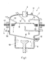
- FIG. 1 of an inventive Process chamber 1 comprises a housing 2, a rotary head 3 with magnetic active elements 30 (e.g. laminated soft iron), a storage / Drive stator 4 with a stator winding 40 and with magnetically active Elements 41 such as sheet metal soft iron parts and permanent magnets (not shown).
- the bearing / drive stator 4 is radially around the rotary head 3 arranged, which carries a wafer W.
- the applicators are preferably slidable and / or designed to be pivotable, which is indicated by corresponding arrows is indicated.
- stator winding 40 comprises a control winding for controlling the Position of the rotary head 3 in the storage level, i.e. in the storage / Drive stator 4, on the other hand, it comprises a drive winding for Driving the rotary head 3, the control winding and drive winding can form common winding
- the functionality and Various embodiments of such a bearingless motor are available known.
- the stator 4 Since the stator 4 is arranged outside the housing 2 of the process chamber is, there is an area of the housing 2 in the air gap between the Turret 3 and the stator 4 is arranged. To keep the air gap as small as possible
- a feed mechanism is also shown, which one Vacuum gripper 7 includes.
- This vacuum gripper 7 is in one in FIG Lock 8 arranged, which comprises two slides 80 and 81.
- the Slider 80 is movable in a plane perpendicular to the drawing plane, that is quasi out of the drawing level and into the drawing level, and opens the lock 8 to the outside. From the outside, the wafer W be applied to the vacuum gripper 7. Then the slider becomes 80 closed and the slide 81 opened.
- the vacuum gripper 7 can then transport the wafer W to the rotary head 3, the applicator, of course 53 must be withdrawn laterally in order to feed the wafer W not to hinder.
- the wafer W is already attached to the rotary head 3 outside the lock 8 or with this is connected, as will be explained in more detail.
- the rotary head 3 is then placed on the vacuum gripper 7 together with the wafer W. applied and then in the interior of the housing 2 Process chamber 1 transported.
- This has the advantage that, firstly, that Attach or connect the wafer W to the rotary head 3 in one place can take place (namely outside the lock), where the rotary head 3 is particularly accessible.
- Finally 1 shows an inlet connection 90 and an outlet connection 91 for supplying and discharging gases and an outlet pipe 92 for Draining liquids.
- Such a process chamber 1 is suitable is therefore also particularly suitable for the production of semiconductors simple structures such as thyristors (e.g. GTO's).
- Fig. 2 shows a further embodiment of an inventive Process chamber.
- the process chamber 1a here comprises the housing 2a, in the interior thereof the rotary head 3a is arranged, which carries the wafer W.
- the turret 3a is carried by the stator 4a and driven in rotation.
- the stator 4a is however, slidable in the axial direction and also to a small extent tiltable, as indicated by the corresponding arrows.
- a nozzle system 54a (applicator) is also provided in FIG. which, for example, a process gas in the interior of the housing 2a can initiate.
- This nozzle system 54a can be designed to be axially displaceable his.
- the process gas is discharged from the interior via the outlet connector 91a the process chamber 1a discharged again.
- a heating coil 55a (applicator), which below the rotary head 3a is arranged, and since the wafer W is freely accessible from below, can homogeneous heating of the wafer W can be achieved.
- other applicators such as electrodes or radiation sources or others Applicators arranged in the interior of the housing of the process chamber his.
- the process chamber 1a shown in FIG. 2 is particularly suitable for CVD (Chemical Vapor Deposition) processes.
- FIG. 3 is a section of an embodiment of a Process chamber 1b shown, in which the stator 4b in an indentation of the housing 2b is arranged. If the diameter of the rotary head 3b small compared to the diameter of the interior of the housing 2b to be held, e.g. around the wafer W together with the rotary head 3b is easier to remove from the interior of the housing 2b this embodiment very advantageous.
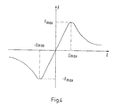
- the relationship between the restoring force F and the axial deflection z from the desired position of the rotary head is shown graphically. It can be seen that in the respective positive or negative axial direction (z-direction), the restoring force initially looks up to a maximum deflection z max or -z max, the amount of the restoring force increases up to a value F max or -F max , at Exceeding this deflection decreases again. This means that if, when the deflection z max or -z max is exceeded, the same force acts on the rotary head in the axial direction that led to the corresponding deflection, the rotary head escapes from the bearing.
- a rotary head 3c which in is essentially annular. This means that the wafer W can be edited from both sides.
- the rotary head 3c has means for sucking the wafer W in the form of a vacuum chamber 31c, in which a negative pressure can be generated via a valve 32c. Thereby the wafer is sucked against the O-rings 33c and 34c. This process can be done outside the interior of the housing. Subsequently the valve 32c is closed so that the negative pressure in the Vacuum chamber 31c is maintained and the wafer W to the O-rings 33c and 34c remains sucked.
- Fig. 6 shows an embodiment of a rotary head 3d, in the interior a disk 35d is arranged, which is provided with passage channels 36d is.
- This disc 35d acts as a nozzle system through which the Wafers W (here from below) are exposed to gases or vapors can.
- the wafer W is in one with the help of the spring-loaded grippers 37d Distance from the disc 35d (here above the disc 35d) kept.
- the Wafer W is therefore accessible from both sides, with the attachment of the wafer W on the rotating head 3d also outside the housing of the process chamber can be done.
- the rotary head 3d thus equipped with the wafer can then be in the interior of the housing of the process chamber can be introduced.
- FIG. 7 shows an embodiment of a process chamber 1e with a Housing 2e, in the interior of which a substantially disc-shaped Turret 3e is arranged.
- This rotary head 3e is with means for Firmly suck the wafer W, in a central area of the turret 3e.
- These means include a valve 32e (e.g. a ball valve). If negative pressure is now generated through the ball valve 32e, then in the vacuum chamber 31e generates a suction pressure under the wafer W, which sucks the wafer W against the O-ring 33e. Then you close the valve 32e, the wafer W remains sucked against the O-ring 33e. As mentioned earlier, this can be done outside the interior of the Housing 2e of the process chamber 1e take place.
- a valve 32e e.g. a ball valve
- a vacuum pump can be provided, which is inductive is fed, as already described with reference to FIG. 5, parts of the Energy of the drive rotating field can be used for supply.
- the turret drops outwards and ends in a tub 38e.
- This tub 38e is on its bottom Passage openings 39e provided. Now becomes one Liquid applicator 51e places a liquid F centrally on the wafer W.
- the liquid F flows due to the rotation of the rotary head 3e over the surface of the wafer W outwards over the wafer edge away, along the sloping areas of the rotary head 3e into the tub 38e and there is a backflow of liquid F which does not run off avoided, so that a homogeneous liquid film on the wafer W can arise.
- a corresponding Outlet connector (not shown) can be provided in the housing which the liquid F can be removed.
- the air gap can be chosen very small, which reduces the losses.
Landscapes
- Container, Conveyance, Adherence, Positioning, Of Wafer (AREA)
- Coating Apparatus (AREA)
- Physical Vapour Deposition (AREA)
Priority Applications (1)
| Application Number | Priority Date | Filing Date | Title |
|---|---|---|---|
| EP99810788.2A EP0989594B1 (fr) | 1998-09-15 | 1999-09-02 | Chambre de traitement |
Applications Claiming Priority (3)
| Application Number | Priority Date | Filing Date | Title |
|---|---|---|---|
| EP98810916 | 1998-09-15 | ||
| EP98810916 | 1998-09-15 | ||
| EP99810788.2A EP0989594B1 (fr) | 1998-09-15 | 1999-09-02 | Chambre de traitement |
Publications (3)
| Publication Number | Publication Date |
|---|---|
| EP0989594A2 true EP0989594A2 (fr) | 2000-03-29 |
| EP0989594A3 EP0989594A3 (fr) | 2005-01-12 |
| EP0989594B1 EP0989594B1 (fr) | 2019-06-19 |
Family
ID=26152028
Family Applications (1)
| Application Number | Title | Priority Date | Filing Date |
|---|---|---|---|
| EP99810788.2A Expired - Lifetime EP0989594B1 (fr) | 1998-09-15 | 1999-09-02 | Chambre de traitement |
Country Status (1)
| Country | Link |
|---|---|
| EP (1) | EP0989594B1 (fr) |
Cited By (6)
| Publication number | Priority date | Publication date | Assignee | Title |
|---|---|---|---|---|
| EP2372749A1 (fr) * | 2010-03-31 | 2011-10-05 | Levitronix GmbH | Dispositif de traitement pour le traitement d'une surface d'un corps |
| EP2415075A4 (fr) * | 2009-03-31 | 2014-01-15 | Lam Res Ag | Dispositif de traitement d'articles de type disque |
| US9044794B2 (en) | 2009-12-31 | 2015-06-02 | Lam Research Ag | Ultrasonic cleaning fluid, method and apparatus |
| US20170018451A1 (en) * | 2015-07-17 | 2017-01-19 | Samsung Electronics Co., Ltd. | Wafer clamping apparatus |
| US10236204B2 (en) | 2011-11-28 | 2019-03-19 | Infineon Technologies Ag | Semiconductor processing system |
| CN113471111A (zh) * | 2021-07-10 | 2021-10-01 | 江苏晟驰微电子有限公司 | 一种孔板钢网印刷实现晶圆玻璃钝化工艺的治具 |
Family Cites Families (5)
| Publication number | Priority date | Publication date | Assignee | Title |
|---|---|---|---|---|
| US5439519A (en) * | 1992-04-28 | 1995-08-08 | Tokyo Ohka Kogyo Co., Ltd. | Solution applying apparatus |
| WO1997003225A1 (fr) * | 1995-07-10 | 1997-01-30 | Cvc Products, Inc. | Appareil de niveau salle blanche, programmable pour la rotation electromagnetique de substrat et procede destine a un equipement de fabrication de composants micro-electroniques |
| US5818137A (en) * | 1995-10-26 | 1998-10-06 | Satcon Technology, Inc. | Integrated magnetic levitation and rotation system |
| US5960555A (en) * | 1996-07-24 | 1999-10-05 | Applied Materials, Inc. | Method and apparatus for purging the back side of a substrate during chemical vapor processing |
| US6157106A (en) * | 1997-05-16 | 2000-12-05 | Applied Materials, Inc. | Magnetically-levitated rotor system for an RTP chamber |
-
1999
- 1999-09-02 EP EP99810788.2A patent/EP0989594B1/fr not_active Expired - Lifetime
Cited By (10)
| Publication number | Priority date | Publication date | Assignee | Title |
|---|---|---|---|---|
| EP2415075A4 (fr) * | 2009-03-31 | 2014-01-15 | Lam Res Ag | Dispositif de traitement d'articles de type disque |
| US8833380B2 (en) | 2009-03-31 | 2014-09-16 | Lam Research Ag | Device for treating disc-like articles |
| US9044794B2 (en) | 2009-12-31 | 2015-06-02 | Lam Research Ag | Ultrasonic cleaning fluid, method and apparatus |
| EP2372749A1 (fr) * | 2010-03-31 | 2011-10-05 | Levitronix GmbH | Dispositif de traitement pour le traitement d'une surface d'un corps |
| US20170287739A1 (en) * | 2010-03-31 | 2017-10-05 | Levitronix Gmbh | Treatment apparatus for treating a surface of a body |
| US10468277B2 (en) | 2010-03-31 | 2019-11-05 | Levitronix Gmbh | Treatment apparatus for treating a surface of a body |
| US10236204B2 (en) | 2011-11-28 | 2019-03-19 | Infineon Technologies Ag | Semiconductor processing system |
| US20170018451A1 (en) * | 2015-07-17 | 2017-01-19 | Samsung Electronics Co., Ltd. | Wafer clamping apparatus |
| US9768051B2 (en) * | 2015-07-17 | 2017-09-19 | Samsung Electronics Co., Ltd. | Wafer clamping apparatus |
| CN113471111A (zh) * | 2021-07-10 | 2021-10-01 | 江苏晟驰微电子有限公司 | 一种孔板钢网印刷实现晶圆玻璃钝化工艺的治具 |
Also Published As
| Publication number | Publication date |
|---|---|
| EP0989594A3 (fr) | 2005-01-12 |
| EP0989594B1 (fr) | 2019-06-19 |
Similar Documents
| Publication | Publication Date | Title |
|---|---|---|
| EP0444714B1 (fr) | Dispositif support pour le traitement d'objet en forme de disque | |
| EP1372186B1 (fr) | Dispositif de traitement de plaquettes | |
| DE69530801T2 (de) | Montageelement und methode zum klemmen eines flachen, dünnen und leitfähigen werkstückes | |
| WO1999004416A1 (fr) | Procede et dispositif pour le traitement de substrats plans, en particulier de pastilles de silicium (tranches) pour la fabrication de composants microelectroniques | |
| DE69909893T2 (de) | Werkzeug für eine kontaktfreie Halterung von plattenförmigen Substraten | |
| EP1179611B1 (fr) | Enceinte pour le transport des substrats | |
| DE60319294T2 (de) | Vorrichtung und Verfahren zur Substratbehandlung | |
| EP0396923B1 (fr) | Table élévatrice et méthode de transportation | |
| DE69706983T2 (de) | Anlage zum behandeln von substraten mit einem plasmastrahl | |
| DE1949767C3 (de) | Vorrichtung zum Herstellen gleichmäßig dicker Schichten | |
| DE3630035C2 (de) | Vorrichtung zum Einladen eines Halbleiterwafers in eine Behandlungskammer und Ionenimplantationsvorrichtung mit dieser Vorrichtung | |
| DE4118973A1 (de) | Vorrichtung zur plasmaunterstuetzten bearbeitung von substraten | |
| EP0989594B1 (fr) | Chambre de traitement | |
| EP0497104B1 (fr) | Magasin pour contenir des pièces en forme de disques, en particulier des disques semi-conducteurs, dans un traitement de surface chimique en bains liquides | |
| DE112016001134T5 (de) | Sputtervorrichtung | |
| EP1186681A1 (fr) | Dispositif de traitement sous vide avec support de substrats couplable | |
| WO2005006409A1 (fr) | Dispositif pour nettoyer des tranches de semi-conducteur ayant subi un traitement chimiomecanique (cmp) | |
| AT408930B (de) | Vorrichtung zur chemischen behandlung von wafern | |
| DE112010003657B4 (de) | Ätzanlage | |
| EP0609489B1 (fr) | Dispositif pour appliquer un masque sur un substrat et/ou pour l'enlever | |
| DD271776A1 (de) | Vorrichtung zur gaszufuehrung und -ableitung fuer die gasphasenbearbeitung von werkstuecken | |
| DE69305725T2 (de) | Magnetron-Zerstäubungsvorrichtung und Dünnfilm-Beschichtungsverfahren | |
| DE69730818T2 (de) | Vorrichtung und verfahren zur kühlung von in einer ionenimplantationsanlage behandelten werkstücken | |
| DE69616131T2 (de) | Verfahren zur Beschichtung eines Substrats durch Sputtern | |
| DE69231293T2 (de) | Verfahren und vorrichtung zur plasmabeschichtung |
Legal Events
| Date | Code | Title | Description |
|---|---|---|---|
| PUAI | Public reference made under article 153(3) epc to a published international application that has entered the european phase |
Free format text: ORIGINAL CODE: 0009012 |
|
| AK | Designated contracting states |
Kind code of ref document: A2 Designated state(s): AT BE CH CY DE DK ES FI FR GB GR IE IT LI LU MC NL PT SE |
|
| AX | Request for extension of the european patent |
Free format text: AL;LT;LV;MK;RO;SI |
|
| RAP1 | Party data changed (applicant data changed or rights of an application transferred) |
Owner name: LEVITRONIX LLC |
|
| PUAL | Search report despatched |
Free format text: ORIGINAL CODE: 0009013 |
|
| AK | Designated contracting states |
Kind code of ref document: A3 Designated state(s): AT BE CH CY DE DK ES FI FR GB GR IE IT LI LU MC NL PT SE |
|
| AX | Request for extension of the european patent |
Extension state: AL LT LV MK RO SI |
|
| 17P | Request for examination filed |
Effective date: 20050705 |
|
| AKX | Designation fees paid |
Designated state(s): AT CH DE GB LI |
|
| 17Q | First examination report despatched |
Effective date: 20060215 |
|
| RAP1 | Party data changed (applicant data changed or rights of an application transferred) |
Owner name: LEVITRONIX TECHNOLOGIES, LLC |
|
| STAA | Information on the status of an ep patent application or granted ep patent |
Free format text: STATUS: EXAMINATION IS IN PROGRESS |
|
| REG | Reference to a national code |
Ref country code: DE Ref legal event code: R079 Ref document number: 59915481 Country of ref document: DE Free format text: PREVIOUS MAIN CLASS: H01L0021000000 Ipc: H01L0021670000 |
|
| GRAP | Despatch of communication of intention to grant a patent |
Free format text: ORIGINAL CODE: EPIDOSNIGR1 |
|
| STAA | Information on the status of an ep patent application or granted ep patent |
Free format text: STATUS: GRANT OF PATENT IS INTENDED |
|
| RIC1 | Information provided on ipc code assigned before grant |
Ipc: H01L 21/67 20060101AFI20190107BHEP Ipc: H01L 21/687 20060101ALI20190107BHEP |
|
| INTG | Intention to grant announced |
Effective date: 20190130 |
|
| GRAS | Grant fee paid |
Free format text: ORIGINAL CODE: EPIDOSNIGR3 |
|
| GRAA | (expected) grant |
Free format text: ORIGINAL CODE: 0009210 |
|
| STAA | Information on the status of an ep patent application or granted ep patent |
Free format text: STATUS: THE PATENT HAS BEEN GRANTED |
|
| AK | Designated contracting states |
Kind code of ref document: B1 Designated state(s): AT CH DE GB LI |
|
| REG | Reference to a national code |
Ref country code: GB Ref legal event code: FG4D Free format text: NOT ENGLISH |
|
| REG | Reference to a national code |
Ref country code: CH Ref legal event code: EP |
|
| REG | Reference to a national code |
Ref country code: DE Ref legal event code: R096 Ref document number: 59915481 Country of ref document: DE |
|
| REG | Reference to a national code |
Ref country code: AT Ref legal event code: REF Ref document number: 1146573 Country of ref document: AT Kind code of ref document: T Effective date: 20190715 |
|
| REG | Reference to a national code |
Ref country code: CH Ref legal event code: PL |
|
| REG | Reference to a national code |
Ref country code: AT Ref legal event code: MK07 Ref document number: 1146573 Country of ref document: AT Kind code of ref document: T Effective date: 20190902 |
|
| REG | Reference to a national code |
Ref country code: GB Ref legal event code: PE20 Expiry date: 20190901 |
|
| PG25 | Lapsed in a contracting state [announced via postgrant information from national office to epo] |
Ref country code: GB Free format text: LAPSE BECAUSE OF EXPIRATION OF PROTECTION Effective date: 20190901 |
|
| REG | Reference to a national code |
Ref country code: DE Ref legal event code: R097 Ref document number: 59915481 Country of ref document: DE |
|
| PLBE | No opposition filed within time limit |
Free format text: ORIGINAL CODE: 0009261 |
|
| STAA | Information on the status of an ep patent application or granted ep patent |
Free format text: STATUS: NO OPPOSITION FILED WITHIN TIME LIMIT |
|
| 26N | No opposition filed |
Effective date: 20200603 |