EP0989662B1 - Boucle de contrôle complètement integrée pour l'allumage d'un transistor de puissance haute tension dans un convertisseur quasi resonant de type 'flyback' - Google Patents
Boucle de contrôle complètement integrée pour l'allumage d'un transistor de puissance haute tension dans un convertisseur quasi resonant de type 'flyback' Download PDFInfo
- Publication number
- EP0989662B1 EP0989662B1 EP98830554A EP98830554A EP0989662B1 EP 0989662 B1 EP0989662 B1 EP 0989662B1 EP 98830554 A EP98830554 A EP 98830554A EP 98830554 A EP98830554 A EP 98830554A EP 0989662 B1 EP0989662 B1 EP 0989662B1
- Authority
- EP
- European Patent Office
- Prior art keywords
- comparator
- voltage
- control
- power
- power transistor
- Prior art date
- Legal status (The legal status is an assumption and is not a legal conclusion. Google has not performed a legal analysis and makes no representation as to the accuracy of the status listed.)
- Expired - Lifetime
Links
- 238000004804 winding Methods 0.000 claims description 15
- 238000004519 manufacturing process Methods 0.000 claims description 3
- 238000000034 method Methods 0.000 claims description 3
- 238000009825 accumulation Methods 0.000 claims description 2
- 239000003990 capacitor Substances 0.000 description 3
- 238000005516 engineering process Methods 0.000 description 3
- 230000001105 regulatory effect Effects 0.000 description 3
- 230000001276 controlling effect Effects 0.000 description 2
- 238000010586 diagram Methods 0.000 description 2
- 230000010355 oscillation Effects 0.000 description 2
- 239000000758 substrate Substances 0.000 description 2
- 230000000694 effects Effects 0.000 description 1
- 230000008030 elimination Effects 0.000 description 1
- 238000003379 elimination reaction Methods 0.000 description 1
- 238000001914 filtration Methods 0.000 description 1
- 238000012544 monitoring process Methods 0.000 description 1
- 238000011084 recovery Methods 0.000 description 1
- 238000004513 sizing Methods 0.000 description 1
Images

Classifications
-
- H—ELECTRICITY
- H02—GENERATION; CONVERSION OR DISTRIBUTION OF ELECTRIC POWER
- H02M—APPARATUS FOR CONVERSION BETWEEN AC AND AC, BETWEEN AC AND DC, OR BETWEEN DC AND DC, AND FOR USE WITH MAINS OR SIMILAR POWER SUPPLY SYSTEMS; CONVERSION OF DC OR AC INPUT POWER INTO SURGE OUTPUT POWER; CONTROL OR REGULATION THEREOF
- H02M3/00—Conversion of DC power input into DC power output
- H02M3/22—Conversion of DC power input into DC power output with intermediate conversion into AC
- H02M3/24—Conversion of DC power input into DC power output with intermediate conversion into AC by static converters
- H02M3/28—Conversion of DC power input into DC power output with intermediate conversion into AC by static converters using discharge tubes with control electrode or semiconductor devices with control electrode to produce the intermediate AC
- H02M3/325—Conversion of DC power input into DC power output with intermediate conversion into AC by static converters using discharge tubes with control electrode or semiconductor devices with control electrode to produce the intermediate AC using devices of a triode or a transistor type requiring continuous application of a control signal
- H02M3/335—Conversion of DC power input into DC power output with intermediate conversion into AC by static converters using discharge tubes with control electrode or semiconductor devices with control electrode to produce the intermediate AC using devices of a triode or a transistor type requiring continuous application of a control signal using semiconductor devices only
- H02M3/33507—Conversion of DC power input into DC power output with intermediate conversion into AC by static converters using discharge tubes with control electrode or semiconductor devices with control electrode to produce the intermediate AC using devices of a triode or a transistor type requiring continuous application of a control signal using semiconductor devices only with automatic control of the output voltage or current, e.g. flyback converters
- H02M3/33523—Conversion of DC power input into DC power output with intermediate conversion into AC by static converters using discharge tubes with control electrode or semiconductor devices with control electrode to produce the intermediate AC using devices of a triode or a transistor type requiring continuous application of a control signal using semiconductor devices only with automatic control of the output voltage or current, e.g. flyback converters with galvanic isolation between input and output of both the power stage and the feedback loop
-
- Y—GENERAL TAGGING OF NEW TECHNOLOGICAL DEVELOPMENTS; GENERAL TAGGING OF CROSS-SECTIONAL TECHNOLOGIES SPANNING OVER SEVERAL SECTIONS OF THE IPC; TECHNICAL SUBJECTS COVERED BY FORMER USPC CROSS-REFERENCE ART COLLECTIONS [XRACs] AND DIGESTS
- Y02—TECHNOLOGIES OR APPLICATIONS FOR MITIGATION OR ADAPTATION AGAINST CLIMATE CHANGE
- Y02B—CLIMATE CHANGE MITIGATION TECHNOLOGIES RELATED TO BUILDINGS, e.g. HOUSING, HOUSE APPLIANCES OR RELATED END-USER APPLICATIONS
- Y02B70/00—Technologies for an efficient end-user side electric power management and consumption
- Y02B70/10—Technologies improving the efficiency by using switched-mode power supplies [SMPS], i.e. efficient power electronics conversion e.g. power factor correction or reduction of losses in power supplies or efficient standby modes
Definitions
- the present invention relates to flyback DC-DC converters, functioning in a quasi resonant or "zero voltage” switch-on mode that is switching on when the voltage on the current terminals of the switching element is in the vicinity of zero volts.
- the quasi resonant functioning mode of flyback DC-DC converters at steady state conditions is particularly efficient because, compared to traditional flyback applications (hard switching mode), allows for a reduction of power dissipation during the switching phases as well as and a reduction of electromagnetic noise.
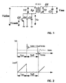
- Fig. 1 shows the basic scheme of a flyback converter for quasi resonant applications.
- the switching element Q1 is indicated as being a bipolar junction transistor though it may be of a different type.
- the D1 and C1 components allow for a quasi resonant functioning, also called QRC mode.
- QRC mode a quasi resonant functioning
- traditional applications such as in hard-switching applications, their function is performed by dedicated snubber or clamper circuits.
- the type of control of the switchings of the (Q1) power switch is similar to that of selfoscillating circuits, commonly named SOPS (Self Oscillating Power Supply), because the switch-on is commanded always in the vicinity of the instant at which the current on the secondary winding of the flyback transformer becomes null.
- SOPS Self Oscillating Power Supply
- Vc Valim + (N1:N2)V2 (being V2 ⁇ Vout)
- the flyback converter belongs to the class of the so-called "zero-voltage quasi resonant" converters.
- US-A-5,796,597 discloses a switch-mode power supply with over-current protection employing a DC-DC flyback converter operating in a tuned switch mode under a current-mode control, on a current pulse-by-current pulse control basis.
- the auxiliary winding AUS is used to self power the control circuit during steady state functioning.
- the power transistor Q1 that implement the switch must withstand voltages that may reach or even exceed a thousand volts.
- a fabrication technology usually referred as Smart Power, suitable for high voltage applications, must be used.
- QRC flyback converters are realized with discrete components, or in the form of an integrated device containing a low voltage control circuit, a high voltage power MOS transistor and eventually some of the passive components, after realized in so-called SMD technology.
- the switch-on under a quasi resonant condition is obtained through an external TDELAY network connected to the AUS auxiliary winding and dimensioned so to synchronize the condition Vc ⁇ 0 with the switching of a comparator of the control circuit contained in the CONTROL-IC block, within the time interval indicated as TDELAY in the diagrams of Fig. 2.
- the integrated circuit of the block CONTROL IC controls an self-oscillating or SOPS functioning mode of the converter.
- the delay block TDELAY with a resistor would produce in a classic hard-switching flyback application.
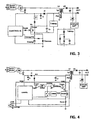
- the QRC function is thus obtained through external networks, which especially in TV applications, where there are large variations of either the supply voltage and the load, necessitate a substantial number of components, as illustrated in the detail of the block TDELAY of Fig. 3, however, other circuit topologies of the delay network may be used, depending on the specific characteristics of the application.
- the scope of the present invention is to provide a QRC quasi resonant selfoscillating flyback DC-DC converter, wherein the synchronization of the switch-on of the power transistor, when the voltage thereon becomes null, is realized with a wholly integrated circuit.
- this objective is obtained by monitoring, rather than the voltage existing on one auxiliary winding of the flyback transformer, as normally done in known circuits, the voltage existing on the current terminal of the power transistor connected to the primary winding of the flyback transformer and by controlling the "set" terminal of a driving flip-flop of the power transistor through a OR logic gate, to an input of which is coupled the output of the comparator of the voltage present on the current node of the power transistor, while the other input of which is coupled, through an integrated TDELAY network, to the output of the comparator of the voltage present on the auxiliary winding in respect to a reference voltage generated by a control circuit of the converter.
- the comparator of the voltage on the current terminal of the power transistor in respect to the ground potential of the circuit is integrated with the same high voltage fabrication technology, that is used to realize high voltage power transistors, that is the components of the input stage of the comparator, which are subject to voltages that may reach and exceed thousands of volts.
- Fig. 4 shows the basic scheme of an embodiment of a quasi resonant self-oscillating flyback converter of the invention.
- the integrated circuit is performed at steady state through the V DD pin by charging a supply capacitor C of great capacitance through a diode D, whose anode, according to a common practice, is coupled to the voltage induced on the AUS auxiliary winding of the transformer. Even though this is not expressly indicated in Fig. 4, there will be means internal or external to the integrated circuit that ensure the charging of the C capacitance during the power-on phase.
- the secondary regulating loop of the output voltage commonly uses, an error amplifier ERROR AMP whose output is coupled, by way of the photo-diode and the photo-transistor, to the relative pin COMP of the integrated circuit to which is connected a compensation capacitor CCOMP of the secondary regulating loop of the output voltage.
- a primary regulating loop whose function is explained in the ensuing description, is realized through the comparator COMP1 which compares the voltage of the auxiliary winding AUS with a pre-established threshold Vrefl, fixed by the control circuitry, represented as a whole by the CONTROL block of the diagram of Fig. 4.
- the secondary control loop of the output voltage switches off the switch POWER by driving the reset of the command flip-flop FF according to a traditional control scheme.
- the synchronization of the switch-on of the POWER switch with the zero crossing instant of the HVC voltage on the current terminal of the power transistor POWER connected to the primary winding of the flyback transformer is effected by controlling the set command of the flip-flop FF through an OR logic gate, a first input of which is coupled to the output of a high voltage comparator HVCOMP of the voltage present existing on the current terminal of the POWER in respect to the ground potential of the circuit.
- Such a voltage coincides with the potential of the substrate of the integrated circuit.
- the output of the first comparator COMP1 is coupled to the second input of the OR logic gate, through a delay network ON DELAY functionally connected in cascade to the output of the COMP1 comparator.
- the quasi resonance condition only exists during steady state operation but not during the start-up and recovery phases.
- the output voltage is reduced and may be zero at the power on instant. Therefore, the voltage induced on the auxiliary winding is insufficiently ample to allow for oscillations of sufficient amplitude.
- control circuit must guarantee the switching on of the switch POWER and this function is performed by the comparator COMP1 through the Oo DELAY block and the OR logic gate.
- the ON DELAY block is designed to ensure that during the steady state selfoscillating functioning, the set of the command flip-flop FF be caused by the switching of the high voltage comparator HVCOMP rather than by the switching of the comparator COMP1. This ensures a POWER switching on of the power transistor POWER in a quasi resonant condition.
- This delay may also be fixed when designing the circuit, similarly to what was done for the delay block Tdelay of the traditional scheme of Fig. 3, in order to switch on the power switch at zero voltage conditions on its terminals.
- Tdelay of the traditional scheme of Fig. 3 in order to switch on the power switch at zero voltage conditions on its terminals.
- the high voltage comparator HVCOMP ensures the correct functioning of the zero voltage quasi resonant converter of the invention, regardless of process spreads of the Lp and Cr values which fix the converter's resonance frequency.
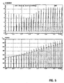
- the circuit of the invention was computer simulated and Figures 5 and 6 report the main waveforms relative to the simulated functioning of the circuit of Fig. 4 with a resistive load coupled to the circuit output OUT.
- Fig. 6 shows the waveforms of the preceding Fig. 5 in greater detail, together with the control voltage of the power transistor switchings and of the output voltages of the high voltage comparator HVCOMP and of the block ON DELAY, respectively, in correspondence of the passage from the hard-switching mode and the QRC mode.
Landscapes
- Engineering & Computer Science (AREA)
- Power Engineering (AREA)
- Dc-Dc Converters (AREA)
Claims (2)
- Convertisseur continu-continu de type "flyback", auto-oscillant de façon quasi résonante (QRC) pendant un fonctionnement à l'état stable, utilisant un transformateur "flyback" pour mémoriser et transférer de l'énergie vers une charge comprenant un enroulement auxiliaire (AUX) dont la tension est comparée par un comparateur (COMP1) à un seuil (VREF1) pour détecter son passage par zéro et en conséquence commuter à l'état passant par l'intermédiaire d'une bascule de commande (FF) un transistor de puissance (POWER) pilotant l'enroulement du transformateur pendant une nouvelle phase de conduction et d'accumulation d'énergie dont la durée est établie par une boucle de commande secondaire de la tension de sortie (ERROR AMP, CONTROL) produisant la commutation à l'ouverture du transistor de puissance pendant une phase de transfert suivante vers la charge de l'énergie stockée dans le transformateur pendant la phase de conduction précédente, caractérisé en ce que le circuit de commande de commutation est complètement intégré et comprend :un second comparateur (HVCOMP) de la tension existant sur la borne de courant du transistor de puissance (POWER) connectée à l'enroulement primaire du transformateur par rapport au potentiel de masse du circuit ;une porte logique (OR) ayant une première entrée connectée à la sortie du second comparateur (HVCOMP) et une sortie couplée à la borne de mise à un de la bascule de commande (FF) ;un circuit de retard (ON DELAY) couplé en cascade sur la sortie du premier comparateur (COMP1) ayant une sortie couplée à une seconde entrée de la porte logique (OR), assurant, dans des conditions de fonctionnement stable du convertisseur, le positionnement de la bascule (FF) par le second comparateur (HVCOMP) plutôt que par le premier comparateur (COMP1).
- Convertisseur selon la revendication 1, caractérisé en ce que le second comparateur (HVCOMP) est réalisé par des composants intégrés selon un procédé de fabrication haute tension.
Priority Applications (3)
| Application Number | Priority Date | Filing Date | Title |
|---|---|---|---|
| DE69814073T DE69814073T2 (de) | 1998-09-23 | 1998-09-23 | Vollständig integrierte Einschaltregelschleife eines Hochspannungsleistungstransistors eines quasiresonanten Sperrwandlers |
| EP98830554A EP0989662B1 (fr) | 1998-09-23 | 1998-09-23 | Boucle de contrôle complètement integrée pour l'allumage d'un transistor de puissance haute tension dans un convertisseur quasi resonant de type 'flyback' |
| US09/400,775 US6078510A (en) | 1998-09-23 | 1999-09-22 | Wholly integrated switch-on control loop of a high voltage power transistor of a quasi resonant flyback converter |
Applications Claiming Priority (1)
| Application Number | Priority Date | Filing Date | Title |
|---|---|---|---|
| EP98830554A EP0989662B1 (fr) | 1998-09-23 | 1998-09-23 | Boucle de contrôle complètement integrée pour l'allumage d'un transistor de puissance haute tension dans un convertisseur quasi resonant de type 'flyback' |
Publications (2)
| Publication Number | Publication Date |
|---|---|
| EP0989662A1 EP0989662A1 (fr) | 2000-03-29 |
| EP0989662B1 true EP0989662B1 (fr) | 2003-05-02 |
Family
ID=8236798
Family Applications (1)
| Application Number | Title | Priority Date | Filing Date |
|---|---|---|---|
| EP98830554A Expired - Lifetime EP0989662B1 (fr) | 1998-09-23 | 1998-09-23 | Boucle de contrôle complètement integrée pour l'allumage d'un transistor de puissance haute tension dans un convertisseur quasi resonant de type 'flyback' |
Country Status (3)
| Country | Link |
|---|---|
| US (1) | US6078510A (fr) |
| EP (1) | EP0989662B1 (fr) |
| DE (1) | DE69814073T2 (fr) |
Cited By (1)
| Publication number | Priority date | Publication date | Assignee | Title |
|---|---|---|---|---|
| DE102011089553A1 (de) * | 2011-12-22 | 2013-06-27 | Robert Bosch Gmbh | Elektronisches Vorschaltgerät für eine Gasentladungslampe |
Families Citing this family (58)
| Publication number | Priority date | Publication date | Assignee | Title |
|---|---|---|---|---|
| US6233165B1 (en) * | 2000-05-15 | 2001-05-15 | Asic Advantage, Inc. | Power converter having a low voltage regulator powered from a high voltage source |
| JP2005519573A (ja) * | 2002-03-01 | 2005-06-30 | コーニンクレッカ フィリップス エレクトロニクス エヌ ヴィ | フリップフロップに基づいた自己発振電源 |
| US7280026B2 (en) | 2002-04-18 | 2007-10-09 | Coldwatt, Inc. | Extended E matrix integrated magnetics (MIM) core |
| FR2871001A1 (fr) * | 2004-05-25 | 2005-12-02 | St Microelectronics Sa | Transformateur a changement de mode et filtre passe-bas |
| US6977824B1 (en) * | 2004-08-09 | 2005-12-20 | System General Corp. | Control circuit for controlling output current at the primary side of a power converter |
| US7362592B2 (en) * | 2004-09-16 | 2008-04-22 | System General Corp. | Switching control circuit for primary-side controlled power converters |
| US7362593B2 (en) * | 2004-09-16 | 2008-04-22 | System General Corp. | Switching control circuit having off-time modulation to improve efficiency of primary-side controlled power supply |
| US7259972B2 (en) * | 2004-10-07 | 2007-08-21 | System General Corporation | Primary-side-control power converter having a switching controller using frequency hopping and voltage and current control loops |
| US7876191B2 (en) | 2005-02-23 | 2011-01-25 | Flextronics International Usa, Inc. | Power converter employing a tapped inductor and integrated magnetics and method of operating the same |
| KR100781359B1 (ko) * | 2005-03-23 | 2007-11-30 | 삼성전자주식회사 | 디지털 제어방식의 고전압 발생장치 |
| US7541793B2 (en) * | 2005-06-07 | 2009-06-02 | Delta Electronics, Inc. | Parallel power supply with active droop current sharing circuit having current limiting function |
| CN101292415B (zh) * | 2005-10-09 | 2010-12-29 | 崇贸科技股份有限公司 | 测量来自功率转换器初级侧的输出电流的设备及方法 |
| JP2008005567A (ja) * | 2006-06-20 | 2008-01-10 | Sanken Electric Co Ltd | スイッチング電源装置 |
| CN101154113B (zh) * | 2006-09-26 | 2010-05-12 | 尼克森微电子股份有限公司 | 电源供应器的准谐振控制电路及其控制方法 |
| US9197132B2 (en) * | 2006-12-01 | 2015-11-24 | Flextronics International Usa, Inc. | Power converter with an adaptive controller and method of operating the same |
| US7675759B2 (en) * | 2006-12-01 | 2010-03-09 | Flextronics International Usa, Inc. | Power system with power converters having an adaptive controller |
| US8564974B2 (en) * | 2007-01-19 | 2013-10-22 | Shindengen Electric Manufacturing Co., Ltd. | Switching power source apparatus |
| US7468649B2 (en) | 2007-03-14 | 2008-12-23 | Flextronics International Usa, Inc. | Isolated power converter |
| US7906941B2 (en) | 2007-06-19 | 2011-03-15 | Flextronics International Usa, Inc. | System and method for estimating input power for a power processing circuit |
| CN101496266B (zh) * | 2007-10-10 | 2012-05-02 | 香港应用科技研究院有限公司 | Dc-dc变换器的低压同步振荡器 |
| KR101468719B1 (ko) * | 2008-03-12 | 2014-12-05 | 페어차일드코리아반도체 주식회사 | 전력 변환기 및 그 구동 방법 |
| WO2009120793A2 (fr) | 2008-03-26 | 2009-10-01 | Enphase Energy, Inc. | Procédé et dispositif permettant d'étendre la plage de commutation sous tension nulle dans un convertisseur cc-cc |
| CN102217181B (zh) * | 2008-11-14 | 2014-09-03 | 伟创力国际美国公司 | 用于同步整流器的驱动器以及采用该驱动器的功率转换器 |
| WO2010083511A1 (fr) | 2009-01-19 | 2010-07-22 | Flextronics International Usa, Inc. | Contrôleur pour un convertisseur de puissance |
| US9088216B2 (en) * | 2009-01-19 | 2015-07-21 | Power Systems Technologies, Ltd. | Controller for a synchronous rectifier switch |
| US9019061B2 (en) | 2009-03-31 | 2015-04-28 | Power Systems Technologies, Ltd. | Magnetic device formed with U-shaped core pieces and power converter employing the same |
| US8514593B2 (en) | 2009-06-17 | 2013-08-20 | Power Systems Technologies, Ltd. | Power converter employing a variable switching frequency and a magnetic device with a non-uniform gap |
| US9077248B2 (en) | 2009-06-17 | 2015-07-07 | Power Systems Technologies Ltd | Start-up circuit for a power adapter |
| US8643222B2 (en) | 2009-06-17 | 2014-02-04 | Power Systems Technologies Ltd | Power adapter employing a power reducer |
| US8638578B2 (en) * | 2009-08-14 | 2014-01-28 | Power System Technologies, Ltd. | Power converter including a charge pump employable in a power adapter |
| US8976549B2 (en) | 2009-12-03 | 2015-03-10 | Power Systems Technologies, Ltd. | Startup circuit including first and second Schmitt triggers and power converter employing the same |
| US8520420B2 (en) | 2009-12-18 | 2013-08-27 | Power Systems Technologies, Ltd. | Controller for modifying dead time between switches in a power converter |
| US9246391B2 (en) | 2010-01-22 | 2016-01-26 | Power Systems Technologies Ltd. | Controller for providing a corrected signal to a sensed peak current through a circuit element of a power converter |
| US8787043B2 (en) | 2010-01-22 | 2014-07-22 | Power Systems Technologies, Ltd. | Controller for a power converter and method of operating the same |
| WO2011116225A1 (fr) | 2010-03-17 | 2011-09-22 | Power Systems Technologies, Ltd. | Système de commande destiné à un convertisseur de puissance et son procédé de fonctionnement |
| US8164928B2 (en) * | 2010-04-28 | 2012-04-24 | System General Corporation | Method and apparatus of operating a primary-side-regulation power converter at both continuous current mode and discontinuous current mode |
| US8792257B2 (en) | 2011-03-25 | 2014-07-29 | Power Systems Technologies, Ltd. | Power converter with reduced power dissipation |
| US8792256B2 (en) | 2012-01-27 | 2014-07-29 | Power Systems Technologies Ltd. | Controller for a switch and method of operating the same |
| US9190898B2 (en) | 2012-07-06 | 2015-11-17 | Power Systems Technologies, Ltd | Controller for a power converter and method of operating the same |
| US9379629B2 (en) | 2012-07-16 | 2016-06-28 | Power Systems Technologies, Ltd. | Magnetic device and power converter employing the same |
| US9099232B2 (en) | 2012-07-16 | 2015-08-04 | Power Systems Technologies Ltd. | Magnetic device and power converter employing the same |
| US9214264B2 (en) | 2012-07-16 | 2015-12-15 | Power Systems Technologies, Ltd. | Magnetic device and power converter employing the same |
| US9106130B2 (en) | 2012-07-16 | 2015-08-11 | Power Systems Technologies, Inc. | Magnetic device and power converter employing the same |
| JP5983172B2 (ja) * | 2012-08-10 | 2016-08-31 | 富士電機株式会社 | スイッチング電源装置及びスイッチング電源装置の制御回路 |
| ITMI20121799A1 (it) * | 2012-10-24 | 2014-04-25 | Greenventive Ltd | Convertitore sepic con isolamento galvanico |
| US9240712B2 (en) | 2012-12-13 | 2016-01-19 | Power Systems Technologies Ltd. | Controller including a common current-sense device for power switches of a power converter |
| KR101350575B1 (ko) | 2012-12-20 | 2014-01-13 | 삼성전기주식회사 | 플라이백 컨버터 |
| KR101388775B1 (ko) | 2012-12-20 | 2014-04-23 | 삼성전기주식회사 | 전원 공급 장치 |
| US9401657B2 (en) * | 2013-03-13 | 2016-07-26 | Power Integrations, Inc. | Input voltage sensor responsive to load conditions |
| CN103347334A (zh) * | 2013-06-27 | 2013-10-09 | 浙江生辉照明有限公司 | 一种led照明装置的驱动电路及驱动方法 |
| US9300206B2 (en) | 2013-11-15 | 2016-03-29 | Power Systems Technologies Ltd. | Method for estimating power of a power converter |
| CN103683867B (zh) * | 2013-12-06 | 2016-03-30 | 深圳市华星光电技术有限公司 | 反激式开关电源电路及应用该电路的背光源驱动装置 |
| CN103997228A (zh) * | 2014-06-11 | 2014-08-20 | 航天长峰朝阳电源有限公司 | 输入端与输出端超高隔离电压的dc/dc电源模块 |
| CN105450023B (zh) * | 2015-12-31 | 2018-09-14 | 杰华特微电子(杭州)有限公司 | 一种开关管控制电路 |
| CN109995254B (zh) * | 2017-12-29 | 2020-12-29 | 东南大学 | 一种提高同步整流原边反馈反激式电源动态性能的方法 |
| US10205381B1 (en) * | 2018-05-10 | 2019-02-12 | Vlt, Inc. | Start-up control in power systems using fixed-ratio power conversion |
| KR102761226B1 (ko) * | 2019-07-12 | 2025-01-31 | 알파 앤드 오메가 세미컨덕터 (케이맨) 리미티드 | 고출력 밀도 충전 응용을 위한 초고속 과도 응답(str) ac/dc 컨버터 |
| CN111969858A (zh) * | 2020-08-25 | 2020-11-20 | 特变电工西安柔性输配电有限公司 | 一种高位取能电源电路及其控制方法 |
Family Cites Families (7)
| Publication number | Priority date | Publication date | Assignee | Title |
|---|---|---|---|---|
| US4462069A (en) * | 1981-08-14 | 1984-07-24 | American Standard Inc. | d.c. To d.c. voltage regulator having an input protection circuit, a d.c. to d.c. inverter, a saturable reactor regulator, and main and auxiliary rectifying and filtering circuits |
| CA1239986A (fr) * | 1985-02-06 | 1988-08-02 | Reliance Electric Company | Commande d'un convertisseur resonant serie |
| DE4122544C1 (fr) * | 1991-07-08 | 1992-07-16 | Braun Ag, 6000 Frankfurt, De | |
| DE59400222D1 (de) * | 1993-02-05 | 1996-05-30 | Siemens Ag | Verfahren zum Begrenzen der Frequenz eines spannungsgesteuerten Oszillators in einer Steuerschaltung eines Resonanzwandler-Schaltnetzteils und Steuerschaltung für ein Resonanzwandler-Schaltnetzteil |
| GB2298532A (en) * | 1995-02-28 | 1996-09-04 | Ibm | Switch mode power supply |
| US5717578A (en) * | 1996-02-07 | 1998-02-10 | Emerging Technologies Corporation | Constant current source employing power conversion circuitry |
| TW344163B (en) * | 1996-09-12 | 1998-11-01 | Thomson Consumer Electronics | Self oscillating proportional drive zero voltage switching power supply |
-
1998
- 1998-09-23 DE DE69814073T patent/DE69814073T2/de not_active Expired - Lifetime
- 1998-09-23 EP EP98830554A patent/EP0989662B1/fr not_active Expired - Lifetime
-
1999
- 1999-09-22 US US09/400,775 patent/US6078510A/en not_active Expired - Lifetime
Cited By (1)
| Publication number | Priority date | Publication date | Assignee | Title |
|---|---|---|---|---|
| DE102011089553A1 (de) * | 2011-12-22 | 2013-06-27 | Robert Bosch Gmbh | Elektronisches Vorschaltgerät für eine Gasentladungslampe |
Also Published As
| Publication number | Publication date |
|---|---|
| DE69814073T2 (de) | 2004-01-22 |
| DE69814073D1 (de) | 2003-06-05 |
| EP0989662A1 (fr) | 2000-03-29 |
| US6078510A (en) | 2000-06-20 |
Similar Documents
| Publication | Publication Date | Title |
|---|---|---|
| EP0989662B1 (fr) | Boucle de contrôle complètement integrée pour l'allumage d'un transistor de puissance haute tension dans un convertisseur quasi resonant de type 'flyback' | |
| US10361633B2 (en) | Control method and device for switching power supplies having more than one control mode | |
| US7692937B2 (en) | Resonant converter and voltage stabilizing method thereof | |
| US5309344A (en) | Dual active clamp, zero voltage switching power converter | |
| US6118675A (en) | Method and apparatus for controlling power transfer in a flyback converter by modulating the power switch off time during transient conditions | |
| KR100378801B1 (ko) | 직류 전원 회로 | |
| US6061252A (en) | Switching power supply device | |
| US7773392B2 (en) | Isolated switching power supply apparatus | |
| US20180248485A1 (en) | Variable blanking frequency for resonant converters | |
| KR20040068239A (ko) | 플라이백 파워 컨버터 | |
| Smith et al. | Controlling a DC-DC converter by using the power MOSFET as a voltage controlled resistor | |
| EP1502349A2 (fr) | Convertisseur llc demi-pont | |
| US12476546B2 (en) | Isolated multiphase series capacitor converters | |
| US6078509A (en) | Multiple output flyback converter having improved cross-regulation and method of operation thereof | |
| JP2769451B2 (ja) | 量子化電力変換装置 | |
| KR101236955B1 (ko) | 스위칭 모드 파워 서플라이 및 그 구동 방법 | |
| CN111030479A (zh) | 有源钳位反激式电源转换器与相关的控制方法 | |
| US12431811B2 (en) | Isolated switching converter with two isolated channels and control method thereof | |
| US5936853A (en) | Power converter having a low-loss clamp and method of operation thereof | |
| TWI669893B (zh) | LLC quasi-resonant switching power supply | |
| US11990840B2 (en) | LLC controller and control method for power converter | |
| CN117595671A (zh) | 供电电路以及应用其的不对称半桥反激变换器 | |
| US12519399B2 (en) | Primary-side controller applied to a power converter and operational method | |
| EP0949751A2 (fr) | Générateur pour machine de soudage à l'arc avec topologie de convertisseur direct et verouillage actif | |
| JP2604302Y2 (ja) | 共振形dc−dcコンバータ |
Legal Events
| Date | Code | Title | Description |
|---|---|---|---|
| PUAI | Public reference made under article 153(3) epc to a published international application that has entered the european phase |
Free format text: ORIGINAL CODE: 0009012 |
|
| AK | Designated contracting states |
Kind code of ref document: A1 Designated state(s): DE FR GB IT |
|
| AX | Request for extension of the european patent |
Free format text: AL;LT;LV;MK;RO;SI |
|
| 17P | Request for examination filed |
Effective date: 20000427 |
|
| AKX | Designation fees paid |
Free format text: DE FR GB IT |
|
| 17Q | First examination report despatched |
Effective date: 20020208 |
|
| GRAH | Despatch of communication of intention to grant a patent |
Free format text: ORIGINAL CODE: EPIDOS IGRA |
|
| GRAH | Despatch of communication of intention to grant a patent |
Free format text: ORIGINAL CODE: EPIDOS IGRA |
|
| GRAA | (expected) grant |
Free format text: ORIGINAL CODE: 0009210 |
|
| AK | Designated contracting states |
Designated state(s): DE FR GB IT |
|
| REG | Reference to a national code |
Ref country code: GB Ref legal event code: FG4D |
|
| REF | Corresponds to: |
Ref document number: 69814073 Country of ref document: DE Date of ref document: 20030605 Kind code of ref document: P |
|
| ET | Fr: translation filed | ||
| PLBE | No opposition filed within time limit |
Free format text: ORIGINAL CODE: 0009261 |
|
| STAA | Information on the status of an ep patent application or granted ep patent |
Free format text: STATUS: NO OPPOSITION FILED WITHIN TIME LIMIT |
|
| 26N | No opposition filed |
Effective date: 20040203 |
|
| PGFP | Annual fee paid to national office [announced via postgrant information from national office to epo] |
Ref country code: IT Payment date: 20060930 Year of fee payment: 9 |
|
| PG25 | Lapsed in a contracting state [announced via postgrant information from national office to epo] |
Ref country code: IT Free format text: LAPSE BECAUSE OF NON-PAYMENT OF DUE FEES Effective date: 20070923 |
|
| PGFP | Annual fee paid to national office [announced via postgrant information from national office to epo] |
Ref country code: GB Payment date: 20120828 Year of fee payment: 15 |
|
| PGFP | Annual fee paid to national office [announced via postgrant information from national office to epo] |
Ref country code: FR Payment date: 20130920 Year of fee payment: 16 |
|
| GBPC | Gb: european patent ceased through non-payment of renewal fee |
Effective date: 20130923 |
|
| PG25 | Lapsed in a contracting state [announced via postgrant information from national office to epo] |
Ref country code: GB Free format text: LAPSE BECAUSE OF NON-PAYMENT OF DUE FEES Effective date: 20130923 |
|
| REG | Reference to a national code |
Ref country code: FR Ref legal event code: ST Effective date: 20150529 |
|
| PG25 | Lapsed in a contracting state [announced via postgrant information from national office to epo] |
Ref country code: FR Free format text: LAPSE BECAUSE OF NON-PAYMENT OF DUE FEES Effective date: 20140930 |
|
| PGFP | Annual fee paid to national office [announced via postgrant information from national office to epo] |
Ref country code: DE Payment date: 20170821 Year of fee payment: 20 |
|
| REG | Reference to a national code |
Ref country code: DE Ref legal event code: R071 Ref document number: 69814073 Country of ref document: DE |