EP0990485A2 - Verfahren zur Freigabeverbesserung einer Halbleiterplatte - Google Patents
Verfahren zur Freigabeverbesserung einer Halbleiterplatte Download PDFInfo
- Publication number
- EP0990485A2 EP0990485A2 EP99116440A EP99116440A EP0990485A2 EP 0990485 A2 EP0990485 A2 EP 0990485A2 EP 99116440 A EP99116440 A EP 99116440A EP 99116440 A EP99116440 A EP 99116440A EP 0990485 A2 EP0990485 A2 EP 0990485A2
- Authority
- EP
- European Patent Office
- Prior art keywords
- polishing pad
- wafer
- slurry
- rotational speed
- increasing
- Prior art date
- Legal status (The legal status is an assumption and is not a legal conclusion. Google has not performed a legal analysis and makes no representation as to the accuracy of the status listed.)
- Granted
Links
Images


Classifications
-
- H—ELECTRICITY
- H10—SEMICONDUCTOR DEVICES; ELECTRIC SOLID-STATE DEVICES NOT OTHERWISE PROVIDED FOR
- H10P—GENERIC PROCESSES OR APPARATUS FOR THE MANUFACTURE OR TREATMENT OF DEVICES COVERED BY CLASS H10
- H10P52/00—Grinding, lapping or polishing of wafers, substrates or parts of devices
-
- H—ELECTRICITY
- H10—SEMICONDUCTOR DEVICES; ELECTRIC SOLID-STATE DEVICES NOT OTHERWISE PROVIDED FOR
- H10P—GENERIC PROCESSES OR APPARATUS FOR THE MANUFACTURE OR TREATMENT OF DEVICES COVERED BY CLASS H10
- H10P90/00—Preparation of wafers not covered by a single main group of this subclass, e.g. wafer reinforcement
- H10P90/12—Preparing bulk and homogeneous wafers
- H10P90/129—Preparing bulk and homogeneous wafers by polishing
-
- B—PERFORMING OPERATIONS; TRANSPORTING
- B24—GRINDING; POLISHING
- B24B—MACHINES, DEVICES, OR PROCESSES FOR GRINDING OR POLISHING; DRESSING OR CONDITIONING OF ABRADING SURFACES; FEEDING OF GRINDING, POLISHING, OR LAPPING AGENTS
- B24B37/00—Lapping machines or devices; Accessories
- B24B37/04—Lapping machines or devices; Accessories designed for working plane surfaces
- B24B37/042—Lapping machines or devices; Accessories designed for working plane surfaces operating processes therefor
-
- B—PERFORMING OPERATIONS; TRANSPORTING
- B24—GRINDING; POLISHING
- B24B—MACHINES, DEVICES, OR PROCESSES FOR GRINDING OR POLISHING; DRESSING OR CONDITIONING OF ABRADING SURFACES; FEEDING OF GRINDING, POLISHING, OR LAPPING AGENTS
- B24B37/00—Lapping machines or devices; Accessories
- B24B37/34—Accessories
- B24B37/345—Feeding, loading or unloading work specially adapted to lapping
Definitions
- This disclosure relates to semiconductor fabrication and more particularly, to an improved method for releasing semiconductor wafers from a polish pad.
- Semiconductor processing includes polishing semiconductor wafers.
- semiconductor polishing includes chemical mechanical polishing or CMP.
- CMP chemical mechanical polishing
- semiconductor wafers are typically placed on a polishing pad.
- a platen supports the polishing pad during processing.
- the wafer is placed on the platen having the polishing pad disposed thereon using a mechanical carrier.
- the platen often provides rotation for polishing the wafer.
- the carrier rotates as well.
- a slurry is introduced onto the polishing pad which includes abrasive materials, such as silicon dioxide particles as well as chemicals for etching the surface of the wafer to provide a polished surface on the wafer.
- the polishing pad includes pores to carry the slurry and distribute the slurry over the wafer.
- the slurry or slurries typically used have high viscosities.
- the carrier removes the wafer from the polishing pad to be cleaned or simply unloaded.
- the slurry viscosity can make the removal of the polishing pad from the wafer difficult since the slurry viscosity causes the polishing pad to stick to the wafer. If the wafer sticks to the polishing pad, this may result in dropping the wafer and cause damage to or even break the wafer. Further, the viscosity of the slurry may cause the wafer to remain in contact with the polishing pad while the carrier attempts to remove it. This may also result in damage to or breakage of the wafer.
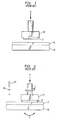
- a carrier 10 for polishing a wafer 12.
- Wafer 12 is releasably coupled to carrier 10 such that wafer 12 may be removed therefrom without damaging wafer 12.
- Carrier 10 is moved in the direction of arrow "B" to bring wafer 12 into contact with a polishing pad 14.
- Polishing pad 14 is disposed on a platen 16.
- Platen 16 may include a turntable for providing a mechanical polishing motion for polishing wafer 12 as will be described herein.
- polishing pad 14 After contacting polishing pad 14, wafer 12 is rotated by carrier 10 as indicated by arrow "A". In addition, platen 16 is rotated in the direction of arrow "C" thereby providing mechanical polishing when abrasives included in slurry 18 are introduced on polishing pad 14.
- Slurry 18 preferably includes silicon dioxide or aluminum oxide abrasives having a primary particle size of about 100 A an up. Slurry 18 is introduced gradually from a slurry feed 20 onto polishing pad 14. A pressure P is applied to carrier 10 to provide a normal force to assist in polishing wafer 12.
- slurry 18 is no longer introduced to polishing pad 14.
- a water polish step is introduced in which water 22 is introduced onto polishing pad 14.
- platen 16 is rotated in the direction of arrow "C" at a rate of about 50 rpm's for about 1-60 seconds prior to carrier 10 separating wafer 12 from pad 14.
- slurries usually have a high viscosity and the introduction of water is not sufficient to provide adequate separation from polishing pad 14.
- Damage to the wafer reduces throughput, and any delay in cleaning the wafer which may result due the difficulty in removing the wafer from the polishing pad may also result in a reduction of wafer yield. Therefore, a need exists for a method for enhancing wafer release from a polish pad after a polishing step.
- a method for releasing semiconductor wafers from a polishing pad.
- the method includes the steps of applying a slurry to a polishing pad, rotating the polishing pad having slurry thereon while applying pressure against a wafer such that the wafer is polished by the slurry, introducing water to the polishing pad, increasing the rotational speed of the polishing pad to remove a portion of the slurry, decreasing the pressure, which may include reducing a back pressure of the wafer by applying a vacuum pressure thereto, during the step of increasing rotational speed to substantially prevent further polishing and removing the wafer from the polishing pad.
- Another method for releasing semiconductor wafers from a polishing pad including the steps of releasably securing a semiconductor wafer to a carrier, applying a slurry to a polishing pad, rotating the carrier and the wafer while applying pressure to the wafer against the polishing pad having slurry thereon such that the wafer is polished by the slurry, rotating the polishing pad such that the wafer is further polished by the slurry, introducing water to the polishing pad to end polishing, increasing the rotational speed of the wafer and the polishing pad to remove a portion of the slurry, decreasing the pressure, which may include reducing a back pressure of the wafer by applying a vacuum pressure thereto, of the wafer against the polishing pad during the step of increasing rotational speed to substantially prevent further polishing and releasing the wafer from the polishing pad by lifting the carrier.
- the step of rotating the polishing pad while applying pressure may include the step of rotating the polishing pad at a rate of about 20 to about 100 rotations per minute.
- the step of rotating the polishing pad while applying pressure may include the step of applying a pressure of between about 2 to 8 psi between the wafer and the polishing pad.
- the step of introducing water to the polishing pad may include the step of discontinuing the slurry to the polishing pad.
- the step of increasing the rotational speed of the polishing pad to remove a portion of the slurry may include the step of increasing the rotational speed of the polishing pad by between about 1.1 times to about 3 times.
- the step of increasing the rotational speed of the polishing pad to remove a portion of the slurry may include the step of increasing the rotational speed of the polishing pad to between about 22 rotations per minute to about 300 rotations per minute.
- the step of decreasing the pressure may include the step of decreasing the pressure to between about 0 to about 3 psi, preferably substantially zero psi.
- The may include the step of introducing a surfactant to the polishing pad to separate the slurry.
- the wafer and the polishing pad may both be rotated and the step of increasing the rotational speed of the wafer and the polishing pad by between about 1.1 times to about 3 times may be included.
- the step of increasing the rotational speed of the wafer and the polishing pad to remove a portion of the slurry includes the step of increasing the rotational speed of the wafer to between about 22 rotations per minute to about 300 rotations per minute.
- the step of increasing the rotational speed of the wafer and the polishing pad to remove a portion of the slurry may include the step of increasing the rotational speed of the polishing pad to between about 22 rotations per minute to about 300 rotations per minute.
- the present invention relates to semiconductor fabrication and more particularly, to method of enhancing release of a semiconductor wafer from a polish pad after a polishing step.
- the present invention provides a method for improving throughput and wafer yield based on a polish step introduced at the end of polishing a wafer.
- the polishing step includes water polishing prior to the removal of the wafer from the polish pad.
- an additional step is included which provides for an increase platen or turntable rotation rate and a smaller normal force exerted by the carrier. In this way, the present invention provides a more easily removed wafer resulting in increased throughput and wafer yield by preventing damage to the wafer and reducing the amount of delay prior to cleaning the wafer.
- a carrier 100 is shown for polishing a wafer 102.
- Wafer 102 is preferably a semiconductor wafer having functional devices formed thereon or being fabricated thereon.
- Wafer 102 is releasably coupled to carrier 100 such that wafer 102 may be removed therefrom without damaging wafer 102.
- Polishing of wafer 102 is conducted as described above with reference to FIGS. 1 and 2.
- wafer 102 is in contact with a polishing pad 104 which is disposed on a platen 106.
- Platen 106 may include a turntable for providing a mechanical polishing motion for polishing wafer 102.
- wafer 102 is rotated by carrier 100 as indicated by arrow "D".
- platen 106 is rotated in the direction of arrow "E" thereby providing mechanical polishing when abrasives included in a slurry 108 are introduced on polishing pad 104.
- Slurry 108 preferably includes silicon dioxide or aluminum oxide abrasives having a primary particle size of 100 A and greater. Other slurries may also be useful.
- Slurry 108 is introduced gradually from a slurry feed 120 onto polishing pad 104.
- a pressure P R is applied to carrier 100 to provide a normal force to assist in polishing wafer 102.
- a water polishing process is performed to remove slurry and end the polishing.
- a water polishing process in accordance with the present invention cuts off slurry 108 and instead introduces water 124. Since slurries are often too viscous to permit proper separation for wafer 102 from polishing pad 104 by carrier 100, the turntable rate of platen 106 is increased by about 1.1 times to about 3 times, i.e., to between about 22 rpm to about 300 rpm. This is performed during the water polishing step described above to separate the slurry and remove the slurry from the wafer. In preferred embodiments, the turntable rate of platen 106 is increased to above 100 rpm. A force provided by pressure P R may also be reduced in conjunction with the increase in speed of the turntable of platen 106 as described in further detail below.
- carrier 100 may be increased in rotational speed to further remove slurry during the water polishing process.
- carrier 100 rotates at the a rate about equal to the increased rate of the turntable, i.e., about 1.1 times to about 3 times, for example, between about 22 rpm to about 300 rpm.
- pressure P R is reduced to between about 0 to about 3 psi, more preferably 0 psi.
- a surfactant such as alcohol, or isopropanol may be introduced though slurry feed 122 to further separate slurry 118 from polishing pad 104.
- the surfactant may be introduced prior to or during the water polishing process.
- a method for releasing semiconductor wafers from a polishing pad includes releasably securing a semiconductor wafer to a carrier in block 200.
- a slurry is introduced to a polishing pad through a slurry feed in block 202.
- the carrier and, therefore, the wafer is rotated while applying pressure to the wafer against the polishing pad in block 204.
- the polishing pad includes pores for carrying the slurry such that the wafer is polished by the slurry when the polishing pad moves relative to the wafer.
- the polishing pad may rotated in addition to the rotation of the carrier to further polish the wafer in block 206.
- water is introduced to the polishing pad to end the polishing process.
- the rotational speed of the wafer and/or the polishing pad is increased to remove a portion of the slurry.
- the pressure of the wafer against the polishing pad is decreased during the step of block 210 to substantially prevent further polishing of the wafer.
- the wafer is released from the polishing pad by lifting the carrier in block 214.
- the carrier preferably includes a vacuum port and the wafer is sealed to the carrier. In this way, a vacuum pressure or back pressure is applied to the backside of the wafer through the vacuum port thereby assisting in lifting the wafer with the carrier.
- polishing slurries are removed and/or reduced in viscosity thereby enhancing the release of a wafer from a polishing pad during processing.
- unloading or cleaning is to be performed on the wafer in accordance with the invention, there is a substantially reduced risk of dropping the wafer or leaving the wafer behind on the polishing pad. This reduced potential damage and/or breakage of the wafer thereby increasing throughput and wafer yield.
Landscapes
- Engineering & Computer Science (AREA)
- Mechanical Engineering (AREA)
- Mechanical Treatment Of Semiconductor (AREA)
- Finish Polishing, Edge Sharpening, And Grinding By Specific Grinding Devices (AREA)
Applications Claiming Priority (2)
| Application Number | Priority Date | Filing Date | Title |
|---|---|---|---|
| US09/161,793 US6132294A (en) | 1998-09-28 | 1998-09-28 | Method of enhancing semiconductor wafer release |
| US161793 | 2002-06-04 |
Publications (3)
| Publication Number | Publication Date |
|---|---|
| EP0990485A2 true EP0990485A2 (de) | 2000-04-05 |
| EP0990485A3 EP0990485A3 (de) | 2002-06-19 |
| EP0990485B1 EP0990485B1 (de) | 2006-06-21 |
Family
ID=22582749
Family Applications (1)
| Application Number | Title | Priority Date | Filing Date |
|---|---|---|---|
| EP99116440A Expired - Lifetime EP0990485B1 (de) | 1998-09-28 | 1999-08-21 | Verfahren zur Freigabeverbesserung einer Halbleiterplatte |
Country Status (6)
| Country | Link |
|---|---|
| US (1) | US6132294A (de) |
| EP (1) | EP0990485B1 (de) |
| JP (1) | JP2000108016A (de) |
| KR (1) | KR100641946B1 (de) |
| DE (1) | DE69932010T2 (de) |
| TW (1) | TW436917B (de) |
Cited By (2)
| Publication number | Priority date | Publication date | Assignee | Title |
|---|---|---|---|---|
| EP1157783A3 (de) * | 2000-05-26 | 2003-10-15 | Ebara Corporation | Polierverfahren und Vorrichtung |
| US6709981B2 (en) | 2000-08-16 | 2004-03-23 | Memc Electronic Materials, Inc. | Method and apparatus for processing a semiconductor wafer using novel final polishing method |
Families Citing this family (15)
| Publication number | Priority date | Publication date | Assignee | Title |
|---|---|---|---|---|
| KR100329208B1 (ko) * | 1998-06-18 | 2002-03-21 | 니시무로 타이죠 | 기능소자와 그 제조방법 및 이 기능소자를 이용한 광디스크장치 |
| US6558228B1 (en) * | 1999-11-15 | 2003-05-06 | Taiwan Semiconductor Manufacturing Company | Method of unloading substrates in chemical-mechanical polishing apparatus |
| US6672943B2 (en) | 2001-01-26 | 2004-01-06 | Wafer Solutions, Inc. | Eccentric abrasive wheel for wafer processing |
| US6632012B2 (en) | 2001-03-30 | 2003-10-14 | Wafer Solutions, Inc. | Mixing manifold for multiple inlet chemistry fluids |
| DE10136742A1 (de) * | 2001-07-27 | 2003-02-13 | Infineon Technologies Ag | Verfahren zum Charakterisieren der Planarisierungseigenschaften einer Verbrauchsmittelkombination in einem chemisch-mechanischen Polierprozeß, Simulationsverfahren und Polierverfahren |
| US6827633B2 (en) * | 2001-12-28 | 2004-12-07 | Ebara Corporation | Polishing method |
| US7037174B2 (en) * | 2002-10-03 | 2006-05-02 | Applied Materials, Inc. | Methods for reducing delamination during chemical mechanical polishing |
| JP2004193289A (ja) * | 2002-12-10 | 2004-07-08 | Ebara Corp | ポリッシング方法 |
| US7081042B2 (en) * | 2004-07-22 | 2006-07-25 | Applied Materials | Substrate removal from polishing tool |
| US20060157450A1 (en) * | 2005-01-20 | 2006-07-20 | Hsin-Kun Chu | Method for improving hss cmp performance |
| CN100468646C (zh) * | 2005-02-02 | 2009-03-11 | 联华电子股份有限公司 | 化学机械研磨方法 |
| CN100537149C (zh) * | 2006-11-28 | 2009-09-09 | 中芯国际集成电路制造(上海)有限公司 | 抛光垫以及化学机械抛光方法 |
| DE102007026292A1 (de) * | 2007-06-06 | 2008-12-11 | Siltronic Ag | Verfahren zur einseitigen Politur nicht strukturierter Halbleiterscheiben |
| JP6209088B2 (ja) * | 2013-01-25 | 2017-10-04 | 株式会社荏原製作所 | 研磨方法および装置 |
| DE102013205448A1 (de) * | 2013-03-27 | 2014-10-16 | Siltronic Ag | Verfahren zum Polieren eines Substrates aus Halbleitermaterial |
Family Cites Families (6)
| Publication number | Priority date | Publication date | Assignee | Title |
|---|---|---|---|---|
| US5320706A (en) * | 1991-10-15 | 1994-06-14 | Texas Instruments Incorporated | Removing slurry residue from semiconductor wafer planarization |
| JP3326642B2 (ja) * | 1993-11-09 | 2002-09-24 | ソニー株式会社 | 基板の研磨後処理方法およびこれに用いる研磨装置 |
| JP2933488B2 (ja) * | 1994-08-10 | 1999-08-16 | 日本電気株式会社 | 研磨方法および研磨装置 |
| JPH0955362A (ja) * | 1995-08-09 | 1997-02-25 | Cypress Semiconductor Corp | スクラッチを減少する集積回路の製造方法 |
| JP3560051B2 (ja) * | 1996-11-15 | 2004-09-02 | 株式会社荏原製作所 | 基板の研磨方法及び装置 |
| US5664990A (en) * | 1996-07-29 | 1997-09-09 | Integrated Process Equipment Corp. | Slurry recycling in CMP apparatus |
-
1998
- 1998-09-28 US US09/161,793 patent/US6132294A/en not_active Expired - Lifetime
-
1999
- 1999-08-21 EP EP99116440A patent/EP0990485B1/de not_active Expired - Lifetime
- 1999-08-21 DE DE69932010T patent/DE69932010T2/de not_active Expired - Lifetime
- 1999-09-23 TW TW088116402A patent/TW436917B/zh not_active IP Right Cessation
- 1999-09-28 JP JP11275095A patent/JP2000108016A/ja not_active Withdrawn
- 1999-09-28 KR KR1019990041462A patent/KR100641946B1/ko not_active Expired - Fee Related
Cited By (4)
| Publication number | Priority date | Publication date | Assignee | Title |
|---|---|---|---|---|
| EP1157783A3 (de) * | 2000-05-26 | 2003-10-15 | Ebara Corporation | Polierverfahren und Vorrichtung |
| US6746312B2 (en) | 2000-05-26 | 2004-06-08 | Ebara Corporation | Polishing method and polishing apparatus |
| KR100777342B1 (ko) * | 2000-05-26 | 2007-11-20 | 가부시키가이샤 에바라 세이사꾸쇼 | 폴리싱 방법 및 폴리싱 장치 |
| US6709981B2 (en) | 2000-08-16 | 2004-03-23 | Memc Electronic Materials, Inc. | Method and apparatus for processing a semiconductor wafer using novel final polishing method |
Also Published As
| Publication number | Publication date |
|---|---|
| KR20000023479A (ko) | 2000-04-25 |
| JP2000108016A (ja) | 2000-04-18 |
| DE69932010D1 (de) | 2006-08-03 |
| KR100641946B1 (ko) | 2006-11-02 |
| EP0990485A3 (de) | 2002-06-19 |
| TW436917B (en) | 2001-05-28 |
| EP0990485B1 (de) | 2006-06-21 |
| DE69932010T2 (de) | 2007-01-11 |
| US6132294A (en) | 2000-10-17 |
Similar Documents
| Publication | Publication Date | Title |
|---|---|---|
| US6132294A (en) | Method of enhancing semiconductor wafer release | |
| US5320706A (en) | Removing slurry residue from semiconductor wafer planarization | |
| US7951718B2 (en) | Edge removal of silicon-on-insulator transfer wafer | |
| US6290579B1 (en) | Fixed abrasive polishing pad | |
| US5424224A (en) | Method of surface protection of a semiconductor wafer during polishing | |
| EP1446263A2 (de) | Verfahren zum polieren der oberfläche eines substrats | |
| JPH09171981A (ja) | 再生半導体ウェハとその再生方法 | |
| JPH02156635A (ja) | ウエーハ用研磨方法 | |
| CN1330797A (zh) | 处理半导体晶片内置后表面损伤的方法 | |
| US6113721A (en) | Method of bonding a semiconductor wafer | |
| CN1674224A (zh) | 衬底处理方法 | |
| WO2004009289A3 (en) | Rising after chemical-mechanical planarization process applied on a wafer | |
| JP2001358107A (ja) | 再生ウェーハから半導体ウェーハへの変換法 | |
| US6300246B1 (en) | Method for chemical mechanical polishing of semiconductor wafer | |
| US6502271B1 (en) | Method and apparatus for cleaning workpieces with uniform relative velocity | |
| JP7438243B2 (ja) | 基板をパッケージングするための平坦化方法 | |
| HK1023535A (en) | Method for enhancing semiconductor wafer release | |
| US6514423B1 (en) | Method for wafer processing | |
| CN1290030A (zh) | 促进半导体晶片释放的方法 | |
| US20040229550A1 (en) | Method for chemical mechanical planarization (CMP) and chemical mechanical cleaning (CMC) of a work piece | |
| JPH10118915A (ja) | 化学的機械研磨方法及び化学的機械研磨装置 | |
| CN116260412B (zh) | 空腔型薄膜体声波谐振器的制造方法 | |
| JPH11239965A (ja) | 化学的機械的研磨及び化学的機械的研磨システムを使用する集積回路の製造方法 | |
| JPH11135616A (ja) | 半導体装置の製造方法 | |
| KR20070028694A (ko) | 화학적 기계적 연마 장치 세정용 도구 |
Legal Events
| Date | Code | Title | Description |
|---|---|---|---|
| PUAI | Public reference made under article 153(3) epc to a published international application that has entered the european phase |
Free format text: ORIGINAL CODE: 0009012 |
|
| AK | Designated contracting states |
Kind code of ref document: A2 Designated state(s): AT BE CH CY DE DK ES FI FR GB GR IE IT LI LU MC NL PT SE |
|
| AX | Request for extension of the european patent |
Free format text: AL;LT;LV;MK;RO;SI |
|
| PUAL | Search report despatched |
Free format text: ORIGINAL CODE: 0009013 |
|
| AK | Designated contracting states |
Kind code of ref document: A3 Designated state(s): AT BE CH CY DE DK ES FI FR GB GR IE IT LI LU MC NL PT SE |
|
| AX | Request for extension of the european patent |
Free format text: AL;LT;LV;MK;RO;SI |
|
| RIC1 | Information provided on ipc code assigned before grant |
Free format text: 7H 01L 21/306 A, 7B 24B 37/04 B, 7H 01L 21/304 - |
|
| 17P | Request for examination filed |
Effective date: 20021217 |
|
| AKX | Designation fees paid |
Designated state(s): DE GB IE |
|
| 17Q | First examination report despatched |
Effective date: 20030306 |
|
| RAP1 | Party data changed (applicant data changed or rights of an application transferred) |
Owner name: INFINEON TECHNOLOGIES AG |
|
| GRAP | Despatch of communication of intention to grant a patent |
Free format text: ORIGINAL CODE: EPIDOSNIGR1 |
|
| GRAS | Grant fee paid |
Free format text: ORIGINAL CODE: EPIDOSNIGR3 |
|
| GRAA | (expected) grant |
Free format text: ORIGINAL CODE: 0009210 |
|
| AK | Designated contracting states |
Kind code of ref document: B1 Designated state(s): DE GB IE |
|
| REG | Reference to a national code |
Ref country code: GB Ref legal event code: FG4D |
|
| REG | Reference to a national code |
Ref country code: IE Ref legal event code: FG4D |
|
| REF | Corresponds to: |
Ref document number: 69932010 Country of ref document: DE Date of ref document: 20060803 Kind code of ref document: P |
|
| PG25 | Lapsed in a contracting state [announced via postgrant information from national office to epo] |
Ref country code: IE Free format text: LAPSE BECAUSE OF NON-PAYMENT OF DUE FEES Effective date: 20060821 |
|
| PGFP | Annual fee paid to national office [announced via postgrant information from national office to epo] |
Ref country code: GB Payment date: 20060824 Year of fee payment: 8 |
|
| REG | Reference to a national code |
Ref country code: HK Ref legal event code: WD Ref document number: 1023535 Country of ref document: HK |
|
| PLBE | No opposition filed within time limit |
Free format text: ORIGINAL CODE: 0009261 |
|
| STAA | Information on the status of an ep patent application or granted ep patent |
Free format text: STATUS: NO OPPOSITION FILED WITHIN TIME LIMIT |
|
| 26N | No opposition filed |
Effective date: 20070322 |
|
| GBPC | Gb: european patent ceased through non-payment of renewal fee |
Effective date: 20070821 |
|
| PG25 | Lapsed in a contracting state [announced via postgrant information from national office to epo] |
Ref country code: GB Free format text: LAPSE BECAUSE OF NON-PAYMENT OF DUE FEES Effective date: 20070821 |
|
| REG | Reference to a national code |
Ref country code: DE Ref legal event code: R081 Ref document number: 69932010 Country of ref document: DE Owner name: POLARIS INNOVATIONS LTD., IE Free format text: FORMER OWNER: QIMONDA AG, 81739 MUENCHEN, DE Ref country code: DE Ref legal event code: R081 Ref document number: 69932010 Country of ref document: DE Owner name: INFINEON TECHNOLOGIES AG, DE Free format text: FORMER OWNER: QIMONDA AG, 81739 MUENCHEN, DE |
|
| REG | Reference to a national code |
Ref country code: DE Ref legal event code: R081 Ref document number: 69932010 Country of ref document: DE Owner name: POLARIS INNOVATIONS LTD., IE Free format text: FORMER OWNER: INFINEON TECHNOLOGIES AG, 85579 NEUBIBERG, DE |
|
| PGFP | Annual fee paid to national office [announced via postgrant information from national office to epo] |
Ref country code: DE Payment date: 20150929 Year of fee payment: 17 |
|
| REG | Reference to a national code |
Ref country code: DE Ref legal event code: R119 Ref document number: 69932010 Country of ref document: DE |
|
| PG25 | Lapsed in a contracting state [announced via postgrant information from national office to epo] |
Ref country code: DE Free format text: LAPSE BECAUSE OF NON-PAYMENT OF DUE FEES Effective date: 20170301 |