EP0991236A2 - Dispositif et méthode d'évaluation de la fréquence centrale d'un signal reçu - Google Patents
Dispositif et méthode d'évaluation de la fréquence centrale d'un signal reçu Download PDFInfo
- Publication number
- EP0991236A2 EP0991236A2 EP99119203A EP99119203A EP0991236A2 EP 0991236 A2 EP0991236 A2 EP 0991236A2 EP 99119203 A EP99119203 A EP 99119203A EP 99119203 A EP99119203 A EP 99119203A EP 0991236 A2 EP0991236 A2 EP 0991236A2
- Authority
- EP
- European Patent Office
- Prior art keywords
- frequency
- power level
- received signal
- obtaining
- peak power
- Prior art date
- Legal status (The legal status is an assumption and is not a legal conclusion. Google has not performed a legal analysis and makes no representation as to the accuracy of the status listed.)
- Withdrawn
Links
Images



Classifications
-
- H—ELECTRICITY
- H04—ELECTRIC COMMUNICATION TECHNIQUE
- H04L—TRANSMISSION OF DIGITAL INFORMATION, e.g. TELEGRAPHIC COMMUNICATION
- H04L27/00—Modulated-carrier systems
- H04L27/18—Phase-modulated carrier systems, i.e. using phase-shift keying
- H04L27/22—Demodulator circuits; Receiver circuits
- H04L27/227—Demodulator circuits; Receiver circuits using coherent demodulation
- H04L27/2275—Demodulator circuits; Receiver circuits using coherent demodulation wherein the carrier recovery circuit uses the received modulated signals
- H04L27/2276—Demodulator circuits; Receiver circuits using coherent demodulation wherein the carrier recovery circuit uses the received modulated signals using frequency multiplication or harmonic tracking
Definitions
- the present invention relates to a frequency estimating system for estimating a center frequency of the carrier wave of a received signal.
- the illustrated frequency estimating system comprises a modulated component removing circuit 11, a Fourier transforming circuit 12, a power converting circuit 13 and a peak detecting circuit 14.
- a received signal having an unknown carrier frequency, for instance, is coupled via an antenna (not shown) to the modulated component removing circuit 11.
- the modulated component removing circuit 11 removes a modulated component from the received signal to obtain a non-modulated signal.
- the Fourier transform circuit 12 performs Fourier transform of the non-modulated signal and outputs the result as a frequency spectrum component.
- the power converting circuit 13 performs power conversion of the frequency spectrum component to feed a resultant power-frequency spectrum to the peak detecting circuit 14.
- the peak detecting circuit 14 detects the peak power level in the power-frequency spectrum and outputs a frequency corresponding to the peak power level as an estimated center frequency fp.
- the received signal is subjected to the rice fading during transmission, a fading component subjected to external disturbance by irregular reflection and a straight component not subject to any external disturbance are combined, and the resultant signal is received.
- a terminal i.e., a mobile terminal
- the fading component and the center frequency of the straight component may fail to be coincident with each other.
- the received signal has a carrier wave spectrum as shown in Fig. 7.
- the fading component and the center frequency of the straight component fail to be coincident.
- the best characteristic can be obtained when the received signal is inputted to a demodulator such that the center frequency of the fading component is zero.
- estimation thereof is necessary.
- the frequency of the straight component is obtained as the estimated frequency (i.e., center frequency). In other words, when the received signal is subjected to fading during transmission, its carrier wave center frequency can not be accurately detected.
- An object of the present invention is to provide a frequency estimating system capable of accurate estimation of the received signal carrier wave center frequency even when the received signal is subjected to the influence of fading or the like in the transmission line.
- a frequency estimating system for estimating a center frequency of carrier wave of a received signal subjected to the influence of fading in the transmission line, comprising a first means for obtaining power-frequency spectrum of the carrier wave of the received signal, a second means for obtaining a peak power level from power-frequency spectrum of the carrier wave and obtaining a peak power level frequency corresponding to the peak power level, and a third means for receiving the carrier wave power-frequency spectrum, the peak power level and the peak power level frequency, detecting a frequency, which is higher than the peak power level frequency and having a power level lower than the peak power level by a predetermined value, as a first lower power level frequency, detecting a frequency, which is lower than the peak power level frequency and having a power level lower than the peak power level by the predetermined value, as a second lower power level frequency, and a third means for obtaining the estimated center frequency by averaging the first and second lower power level frequencies.
- the predetermined value may be 10 dB.
- the third means includes a first detector for detecting the first lower power level frequency, a second detector for detecting the second lower power level frequency, and an averaging circuit for obtaining the center frequency by averaging the first and second lower power level frequencies.
- the received signal contains a predetermined fixed signal series inserted therein, and the first means includes an inverse modulator for inversely modulating the received signal according to the fixed signal series to obtain a non-modulated signal free from any modulated component, a Fourier transform circuit for executing Fourier transform of the non-modulated signal to obtain a frequency spectrum, and a power converter for power converting the frequency spectrum to obtain the power-frequency spectrum.
- the first means includes an inverse modulator for inversely modulating the received signal according to the fixed signal series to obtain a non-modulated signal free from any modulated component, a Fourier transform circuit for executing Fourier transform of the non-modulated signal to obtain a frequency spectrum, and a power converter for power converting the frequency spectrum to obtain the power-frequency spectrum.
- the first means includes a demodulator for demodulating the received signal to obtain a demodulated signal, an inverse modulator for inversely modulating the received signal according to the demodulated signal to obtain a non-modulated signal free from any modulated component, a Fourier transform circuit for executing Fourier transform of the non-modulated signal to obtain a frequency spectrum, and a power converter for power converting the frequency spectrum to obtain the power-frequency spectrum.
- the first means includes a frequency multiplier for frequency multiplying the received signal to obtain a nonmodulated signal free from any modulated component, a Fourier transform circuit for executing Fourier transform of the non-modulated signal to obtain a frequency spectrum, and a power converter for power converting the frequency spectrum to obtain the power-frequency spectrum.
- a frequency estimating method comprising steps of: obtaining a peak power level from power-frequency spectrum of carrier wave of received signal; obtaining a first and second frequencies having higher and lower than the peak power level frequency and having a power level lower than the peak power level by a predetermined value; and obtaining an estimated center frequency by averaging the first and second frequencies.
- a frequency estimating method comprising steps of: obtaining a non-modulated signal free from any modulated component by inversely modulating a received signal on the basis of a predetermined fixed signal series inserted in the received signal; obtaining a peak power level from power-frequency spectrum of carrier wave of the received signal based on the non-modulated signal; obtaining a first and second frequencies having higher and lower than the peak power level frequency and having a power level lower than the peak power level by a predetermined value; and obtaining an estimated center frequency by averaging the first and second frequencies.
- a frequency estimating method comprising steps of: demodulating a received signal to obtain a demodulated signal; inversely modulating the received signal according to the demodulated signal to obtain a non-modulated signal free from any modulated component; obtaining a peak power level from power-frequency spectrum of carrier wave of the received signal based on the non-modulated signal; obtaining a first and second frequencies having higher and lower than the peak power level frequency and having a power level lower than the peak power level by a predetermined value; and obtaining an estimated center frequency by averaging the first and second frequencies.
- a frequency estimating method comprising steps of: frequency multiplying a received signal to obtain a non-modulated signal tree from any modulated component; obtaining a peak power level from power-frequency spectrum of carrier wave of the received signal based on the non-modulated signal; obtaining a first and second frequencies having higher and lower than the peak power level frequency and having a power level lower than the peak power level by a predetermined value; and obtaining an estimated center frequency by averaging the first and second frequencies.
- the predetermined value may be 10 dB.
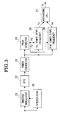
- the illustrated frequency estimating system comprises an inverse modulator 21, Fourier transforming circuit 22, a power converter 23, a peak detector 24, a first and a second lower power level frequency detector 25 and 26 and an averaging circuit 27.
- a predetermined signal series or a so-called unique word are inserted in the received signal and that the timing of receiving the unique word on the receiving side is known.
- the received signal is supplied to the inverting amplifier 21, and a unique word is also supplied thereto separately.
- the inverse modulator 21 inversely modulates a unique ward portion of the received signal to remove the modulated component and obtain a non-modulated signal.
- the Fourier transform circuit 22 performs Fourier transform of the non-modulated signal.
- the power converter 23 power converts each frequency component of the output of the Fourier transform circuit 22, thus obtaining a power-frequency spectrum.
- Fig. 2 shows an example of the power-frequency spectrum obtained in this way. As shown, the power-frequency spectrum is spread due to the fading, and its center frequency is not coincident with the peak power level frequency.
- the peak detector 24 detects the peak power level (i.e., maximum power level) Pp in the power spectrum, and obtains a frequency fp corresponding to the detected peak power level Pp.
- the peak detector 24 supplies the frequency (i.e., peak power level frequency) fp and the peak power level Pp to the first and second lower power level frequency detectors 25 and 26.
- the power converter 23 feeds the power spectrum to the first and second lower power level frequency detectors 25 and 26.
- the predetermined value is prescribed to be at a point of -10 dB.
- the first predetermined value detector 25 detects a frequency, which is higher than the peak power level frequency fp and having a power level lower than the peak power level Pp by 10 dB, as a first lower power level frequency fu. That is, the first lower power level frequency detector 25 detects the first lower power level frequency fu higher than the peak power level frequency and corresponding to the power level (Pp - 10 dB).
- the second lower power level frequency detector 26 detects a frequency which is lower than the peak power level frequency Pp and corresponding to a power level lower than the peak power level Pp by 10 dB, as a second lower power level frequency fd. That is, the second lower power level frequency detector 26 detects the second lower power level frequency fd lower than the peak power level frequency fp and having the power level (Pp - 10 dB).
- the first and second lower power level frequencies fu and fd are supplied to the averaging circuit 27.
- the averaging circuit 27 obtains the mean frequency of the first and second lower power level frequencies fu and fd, and outputs the mean frequency as an estimated center frequency fc of the received signal carrier wave.
- the first and second lower power level frequencies fu and fd correspond to the opposite edge frequencies of the spread carrier wave frequency range, and their mean frequency (fu + fd)/2 substantially coincides with the center frequency fc.
- the illustrated frequency estimating system is applied to the case where the received signal contains no fixed pattern (or unique word).
- a demodulator 28 is additionally provided.
- the received signal is coupled to the inverse modulator 21 and the demodulator 28.
- the demodulator 28 demodulates the received signal and feeds the resultant demodulated signal to the inverse modulator 21.
- the inverse modulator 21 inversely modulates the received signal with the demodulated signal to remove the modulated component, and feeds the resultant non-modulated signal to the Fourier transform circuit 22.
- the subsequent process is the same as described before in connection with Fig. 2, and will not be described.
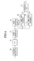
- FIG. 4 A further embodiment of the frequency estimating system according to the present invention will be described with reference to Fig. 4.
- components like those in the frequency estimating system as shown in Fig. 2 are designated by like reference numerals, and will not be described.
- a frequency multiplier 29 is provided instead of the inverse modulator 21.
- the frequency multiplier 29 frequency multiplies the received signal to remove the modulated component, and supplies the non-modulated component to the Fourier transform circuit 22.
- the subsequent processing is the same as described before, and will not be described.
- Fig. 5 shows an error rate characteristic plotted against the shift frequency of the received signal.
- labeled f0 is the center frequency of the spread frequency range of the received signal due to the fading
- labeled -f1 is the peak power level frequency.
- the characteristic is the best when the shift frequency f is -f0. It will be seen that the error rate characteristic can be improved by estimating the center frequency of the received signal subjected to the fading with either of the frequency estimating systems described above and compensating the frequency of the received signal according to the result of the estimation.
Landscapes
- Engineering & Computer Science (AREA)
- Computer Networks & Wireless Communication (AREA)
- Signal Processing (AREA)
- Digital Transmission Methods That Use Modulated Carrier Waves (AREA)
- Monitoring And Testing Of Transmission In General (AREA)
Applications Claiming Priority (2)
| Application Number | Priority Date | Filing Date | Title |
|---|---|---|---|
| JP27355698A JP3296421B2 (ja) | 1998-09-28 | 1998-09-28 | 周波数推定装置 |
| JP27355698 | 1998-09-28 |
Publications (2)
| Publication Number | Publication Date |
|---|---|
| EP0991236A2 true EP0991236A2 (fr) | 2000-04-05 |
| EP0991236A3 EP0991236A3 (fr) | 2001-09-05 |
Family
ID=17529462
Family Applications (1)
| Application Number | Title | Priority Date | Filing Date |
|---|---|---|---|
| EP99119203A Withdrawn EP0991236A3 (fr) | 1998-09-28 | 1999-09-27 | Dispositif et méthode d'évaluation de la fréquence centrale d'un signal reçu |
Country Status (3)
| Country | Link |
|---|---|
| US (1) | US6232761B1 (fr) |
| EP (1) | EP0991236A3 (fr) |
| JP (1) | JP3296421B2 (fr) |
Cited By (3)
| Publication number | Priority date | Publication date | Assignee | Title |
|---|---|---|---|---|
| EP1209910A3 (fr) * | 2000-11-28 | 2004-03-03 | Mitsubishi Denki Kabushiki Kaisha | Appareil de réception |
| EP1383288A3 (fr) * | 2002-07-16 | 2006-11-15 | Rohde & Schwarz GmbH & Co. KG | Procédé et dispositif pour mesurer le débit de symboles d'un signal à fréquence élevée numériquement modulée |
| CN113162652A (zh) * | 2021-04-29 | 2021-07-23 | 陕西凌云电器集团有限公司 | 一种扩频信号频率检测方法及模块 |
Families Citing this family (6)
| Publication number | Priority date | Publication date | Assignee | Title |
|---|---|---|---|---|
| EP1589681B1 (fr) | 2003-01-30 | 2010-12-22 | Fujitsu Limited | Appareil d'estimation de frequence d'evanouissement |
| WO2007036866A2 (fr) * | 2005-09-27 | 2007-04-05 | Nxp B.V. | Procede, programme et module pour estimer une frequence doppler maximale et un decalage de frequence, recepteur comprenant le module |
| EP2533069A1 (fr) * | 2011-06-10 | 2012-12-12 | Sony Corporation | Unité de traitement de signal et procédé |
| JP5712992B2 (ja) * | 2012-10-30 | 2015-05-07 | 日本電気株式会社 | 雑音電力測定装置および雑音電力測定方法 |
| CN104062498B (zh) * | 2014-04-11 | 2017-10-20 | 哈尔滨理工大学 | 对称频谱信号的中心频率的质心估计方法 |
| CN116148779B (zh) * | 2023-04-19 | 2023-08-25 | 隔空(上海)智能科技有限公司 | 一种工频滤波方法、系统、存储介质及电子设备 |
Family Cites Families (6)
| Publication number | Priority date | Publication date | Assignee | Title |
|---|---|---|---|---|
| JP2993541B2 (ja) | 1992-03-02 | 1999-12-20 | 日本電気株式会社 | 高速同期復調装置 |
| JP2932861B2 (ja) * | 1992-10-13 | 1999-08-09 | 日本電気株式会社 | 位相同期検出回路 |
| US5598441A (en) * | 1994-10-13 | 1997-01-28 | Westinghouse Electric Corp. | Carrier acquisition technique for mobile radio QPSK demodulator |
| JP3271504B2 (ja) * | 1996-02-02 | 2002-04-02 | 三菱電機株式会社 | 周波数推定回路およびそれを用いたafc回路 |
| US5799038A (en) * | 1996-04-30 | 1998-08-25 | Advantest Corporation | Method for measuring modulation parameters of digital quadrature-modulated signal |
| CA2214163C (fr) * | 1996-09-27 | 2001-07-31 | Nec Corporation | Methode et appareil de demodulatioin sans preambule |
-
1998
- 1998-09-28 JP JP27355698A patent/JP3296421B2/ja not_active Expired - Fee Related
-
1999
- 1999-09-27 EP EP99119203A patent/EP0991236A3/fr not_active Withdrawn
- 1999-09-27 US US09/405,008 patent/US6232761B1/en not_active Expired - Fee Related
Cited By (4)
| Publication number | Priority date | Publication date | Assignee | Title |
|---|---|---|---|---|
| EP1209910A3 (fr) * | 2000-11-28 | 2004-03-03 | Mitsubishi Denki Kabushiki Kaisha | Appareil de réception |
| US6873369B2 (en) | 2000-11-28 | 2005-03-29 | Mitsubishi Denki Kabushiki Kaisha | Receiving apparatus |
| EP1383288A3 (fr) * | 2002-07-16 | 2006-11-15 | Rohde & Schwarz GmbH & Co. KG | Procédé et dispositif pour mesurer le débit de symboles d'un signal à fréquence élevée numériquement modulée |
| CN113162652A (zh) * | 2021-04-29 | 2021-07-23 | 陕西凌云电器集团有限公司 | 一种扩频信号频率检测方法及模块 |
Also Published As
| Publication number | Publication date |
|---|---|
| EP0991236A3 (fr) | 2001-09-05 |
| JP3296421B2 (ja) | 2002-07-02 |
| US6232761B1 (en) | 2001-05-15 |
| JP2000106576A (ja) | 2000-04-11 |
Similar Documents
| Publication | Publication Date | Title |
|---|---|---|
| JP2751840B2 (ja) | 信号検出装置 | |
| EP0113231B1 (fr) | Système de transmission de données comportant des modems couplés à un moyen de communication commun | |
| EP0609717B1 (fr) | Démodulateur de porteur | |
| US5291081A (en) | Apparatus for detection of non-modulated signal and frequency acquisition | |
| US6005891A (en) | System for testing signal transmission/reception apparatus | |
| US5732105A (en) | Method of estimating signal quality in a DPSK demodulator | |
| US6232761B1 (en) | Frequency estimating system | |
| JP3271504B2 (ja) | 周波数推定回路およびそれを用いたafc回路 | |
| US6829291B1 (en) | Receiving apparatus and synchronization capturing method | |
| JPH07297870A (ja) | Tdmaデータ受信装置 | |
| US6411664B1 (en) | Correlation detecting apparatus, its detecting method and communication apparatus and its communication method | |
| JP3982662B2 (ja) | 受信方法及び高周波信号受信機 | |
| JPH1146179A (ja) | スペクトル拡散通信システム | |
| US6002711A (en) | Spread spectrum communication system for error compensation of carrier frequency | |
| US4988951A (en) | Quadrature phase demodulator capable of operating under a wide input dynamic range | |
| US7746960B2 (en) | Apparatus and method for compensating for I/Q mismatch in TDD system | |
| JP2848420B2 (ja) | バースト信号検出装置および方法 | |
| US6181750B1 (en) | Apparatus for estimating the frequency difference existing between the carrier frequency of a digital signal and the frequency of a receiver local oscillator | |
| US5524282A (en) | Apparatus and method for detecting place of burst signals in time division multiplex communication system | |
| US5247308A (en) | Detection and characterization of LPI signals | |
| JP3789157B2 (ja) | 周波数誤差推定装置 | |
| JPS6359612B2 (fr) | ||
| EP4293967A1 (fr) | Dispositif d'estimation d'écart de fréquence et procédé d'estimation d'écart de fréquence | |
| US20010019582A1 (en) | Frequency modulation method and modem unit employing such method | |
| KR100309591B1 (ko) | 코드분할다중접속통신시스템의코히런트데이터복조장치및방법 |
Legal Events
| Date | Code | Title | Description |
|---|---|---|---|
| PUAI | Public reference made under article 153(3) epc to a published international application that has entered the european phase |
Free format text: ORIGINAL CODE: 0009012 |
|
| AK | Designated contracting states |
Kind code of ref document: A2 Designated state(s): AT BE CH CY DE DK ES FI FR GB GR IE IT LI LU MC NL PT SE |
|
| AX | Request for extension of the european patent |
Free format text: AL;LT;LV;MK;RO;SI |
|
| PUAL | Search report despatched |
Free format text: ORIGINAL CODE: 0009013 |
|
| AK | Designated contracting states |
Kind code of ref document: A3 Designated state(s): AT BE CH CY DE DK ES FI FR GB GR IE IT LI LU MC NL PT SE |
|
| AX | Request for extension of the european patent |
Free format text: AL;LT;LV;MK;RO;SI |
|
| RIC1 | Information provided on ipc code assigned before grant |
Free format text: 7H 04L 27/227 A, 7H 04L 27/00 B |
|
| 17P | Request for examination filed |
Effective date: 20010725 |
|
| AKX | Designation fees paid |
Free format text: DE FR GB |
|
| 17Q | First examination report despatched |
Effective date: 20040609 |
|
| STAA | Information on the status of an ep patent application or granted ep patent |
Free format text: STATUS: THE APPLICATION IS DEEMED TO BE WITHDRAWN |
|
| 18D | Application deemed to be withdrawn |
Effective date: 20051123 |