EP0991977B1 - Dispositif a cristaux liquides - Google Patents
Dispositif a cristaux liquides Download PDFInfo
- Publication number
- EP0991977B1 EP0991977B1 EP98930912A EP98930912A EP0991977B1 EP 0991977 B1 EP0991977 B1 EP 0991977B1 EP 98930912 A EP98930912 A EP 98930912A EP 98930912 A EP98930912 A EP 98930912A EP 0991977 B1 EP0991977 B1 EP 0991977B1
- Authority
- EP
- European Patent Office
- Prior art keywords
- layer
- liquid crystal
- compensator
- crystal material
- cell wall
- Prior art date
- Legal status (The legal status is an assumption and is not a legal conclusion. Google has not performed a legal analysis and makes no representation as to the accuracy of the status listed.)
- Expired - Lifetime
Links
- 239000004973 liquid crystal related substance Substances 0.000 title claims description 47
- 239000000463 material Substances 0.000 claims description 33
- 210000002421 cell wall Anatomy 0.000 claims description 22
- 230000003287 optical effect Effects 0.000 claims description 12
- 238000010276 construction Methods 0.000 claims description 4
- 229920000642 polymer Polymers 0.000 claims description 4
- 239000004986 Cholesteric liquid crystals (ChLC) Substances 0.000 claims description 3
- 239000004988 Nematic liquid crystal Substances 0.000 claims description 3
- 229910021532 Calcite Inorganic materials 0.000 claims description 2
- 229920000106 Liquid crystal polymer Polymers 0.000 claims description 2
- 239000004977 Liquid-crystal polymers (LCPs) Substances 0.000 claims description 2
- 230000005684 electric field Effects 0.000 claims description 2
- 239000010453 quartz Substances 0.000 claims description 2
- VYPSYNLAJGMNEJ-UHFFFAOYSA-N silicon dioxide Inorganic materials O=[Si]=O VYPSYNLAJGMNEJ-UHFFFAOYSA-N 0.000 claims description 2
- 210000004027 cell Anatomy 0.000 description 24
- 230000005540 biological transmission Effects 0.000 description 23
- 239000011159 matrix material Substances 0.000 description 7
- 238000000034 method Methods 0.000 description 3
- 238000004381 surface treatment Methods 0.000 description 3
- IIZPXYDJLKNOIY-JXPKJXOSSA-N 1-palmitoyl-2-arachidonoyl-sn-glycero-3-phosphocholine Chemical compound CCCCCCCCCCCCCCCC(=O)OC[C@H](COP([O-])(=O)OCC[N+](C)(C)C)OC(=O)CCC\C=C/C\C=C/C\C=C/C\C=C/CCCCC IIZPXYDJLKNOIY-JXPKJXOSSA-N 0.000 description 2
- 230000008859 change Effects 0.000 description 2
- 239000010408 film Substances 0.000 description 2
- 239000011521 glass Substances 0.000 description 2
- 230000006872 improvement Effects 0.000 description 2
- 229940067606 lecithin Drugs 0.000 description 2
- 235000010445 lecithin Nutrition 0.000 description 2
- 239000000787 lecithin Substances 0.000 description 2
- 230000008569 process Effects 0.000 description 2
- 125000006850 spacer group Chemical group 0.000 description 2
- XOLBLPGZBRYERU-UHFFFAOYSA-N tin dioxide Chemical compound O=[Sn]=O XOLBLPGZBRYERU-UHFFFAOYSA-N 0.000 description 2
- 230000007704 transition Effects 0.000 description 2
- 238000011282 treatment Methods 0.000 description 2
- 101100459259 Arabidopsis thaliana MYC2 gene Proteins 0.000 description 1
- VYZAMTAEIAYCRO-UHFFFAOYSA-N Chromium Chemical compound [Cr] VYZAMTAEIAYCRO-UHFFFAOYSA-N 0.000 description 1
- OWYWGLHRNBIFJP-UHFFFAOYSA-N Ipazine Chemical compound CCN(CC)C1=NC(Cl)=NC(NC(C)C)=N1 OWYWGLHRNBIFJP-UHFFFAOYSA-N 0.000 description 1
- 239000004642 Polyimide Substances 0.000 description 1
- 239000004990 Smectic liquid crystal Substances 0.000 description 1
- 238000004873 anchoring Methods 0.000 description 1
- 239000011324 bead Substances 0.000 description 1
- 230000008901 benefit Effects 0.000 description 1
- 230000003098 cholesteric effect Effects 0.000 description 1
- 210000002858 crystal cell Anatomy 0.000 description 1
- 230000001419 dependent effect Effects 0.000 description 1
- 239000006185 dispersion Substances 0.000 description 1
- 238000004049 embossing Methods 0.000 description 1
- QSHDDOUJBYECFT-UHFFFAOYSA-N mercury Chemical compound [Hg] QSHDDOUJBYECFT-UHFFFAOYSA-N 0.000 description 1
- 229910052753 mercury Inorganic materials 0.000 description 1
- 239000000203 mixture Substances 0.000 description 1
- 238000000206 photolithography Methods 0.000 description 1
- 229920002120 photoresistant polymer Polymers 0.000 description 1
- 229920001721 polyimide Polymers 0.000 description 1
- 230000005855 radiation Effects 0.000 description 1
- 239000004094 surface-active agent Substances 0.000 description 1
- 239000010409 thin film Substances 0.000 description 1
- XLYOFNOQVPJJNP-UHFFFAOYSA-N water Substances O XLYOFNOQVPJJNP-UHFFFAOYSA-N 0.000 description 1
Images


Classifications
-
- G—PHYSICS
- G02—OPTICS
- G02F—OPTICAL DEVICES OR ARRANGEMENTS FOR THE CONTROL OF LIGHT BY MODIFICATION OF THE OPTICAL PROPERTIES OF THE MEDIA OF THE ELEMENTS INVOLVED THEREIN; NON-LINEAR OPTICS; FREQUENCY-CHANGING OF LIGHT; OPTICAL LOGIC ELEMENTS; OPTICAL ANALOGUE/DIGITAL CONVERTERS
- G02F1/00—Devices or arrangements for the control of the intensity, colour, phase, polarisation or direction of light arriving from an independent light source, e.g. switching, gating or modulating; Non-linear optics
- G02F1/01—Devices or arrangements for the control of the intensity, colour, phase, polarisation or direction of light arriving from an independent light source, e.g. switching, gating or modulating; Non-linear optics for the control of the intensity, phase, polarisation or colour
- G02F1/13—Devices or arrangements for the control of the intensity, colour, phase, polarisation or direction of light arriving from an independent light source, e.g. switching, gating or modulating; Non-linear optics for the control of the intensity, phase, polarisation or colour based on liquid crystals, e.g. single liquid crystal display cells
- G02F1/137—Devices or arrangements for the control of the intensity, colour, phase, polarisation or direction of light arriving from an independent light source, e.g. switching, gating or modulating; Non-linear optics for the control of the intensity, phase, polarisation or colour based on liquid crystals, e.g. single liquid crystal display cells characterised by the electro-optical or magneto-optical effect, e.g. field-induced phase transition, orientation effect, guest-host interaction or dynamic scattering
- G02F1/139—Devices or arrangements for the control of the intensity, colour, phase, polarisation or direction of light arriving from an independent light source, e.g. switching, gating or modulating; Non-linear optics for the control of the intensity, phase, polarisation or colour based on liquid crystals, e.g. single liquid crystal display cells characterised by the electro-optical or magneto-optical effect, e.g. field-induced phase transition, orientation effect, guest-host interaction or dynamic scattering based on orientation effects in which the liquid crystal remains transparent
- G02F1/1396—Devices or arrangements for the control of the intensity, colour, phase, polarisation or direction of light arriving from an independent light source, e.g. switching, gating or modulating; Non-linear optics for the control of the intensity, phase, polarisation or colour based on liquid crystals, e.g. single liquid crystal display cells characterised by the electro-optical or magneto-optical effect, e.g. field-induced phase transition, orientation effect, guest-host interaction or dynamic scattering based on orientation effects in which the liquid crystal remains transparent the liquid crystal being selectively controlled between a twisted state and a non-twisted state, e.g. TN-LC cell
-
- G—PHYSICS
- G02—OPTICS
- G02F—OPTICAL DEVICES OR ARRANGEMENTS FOR THE CONTROL OF LIGHT BY MODIFICATION OF THE OPTICAL PROPERTIES OF THE MEDIA OF THE ELEMENTS INVOLVED THEREIN; NON-LINEAR OPTICS; FREQUENCY-CHANGING OF LIGHT; OPTICAL LOGIC ELEMENTS; OPTICAL ANALOGUE/DIGITAL CONVERTERS
- G02F1/00—Devices or arrangements for the control of the intensity, colour, phase, polarisation or direction of light arriving from an independent light source, e.g. switching, gating or modulating; Non-linear optics
- G02F1/01—Devices or arrangements for the control of the intensity, colour, phase, polarisation or direction of light arriving from an independent light source, e.g. switching, gating or modulating; Non-linear optics for the control of the intensity, phase, polarisation or colour
- G02F1/13—Devices or arrangements for the control of the intensity, colour, phase, polarisation or direction of light arriving from an independent light source, e.g. switching, gating or modulating; Non-linear optics for the control of the intensity, phase, polarisation or colour based on liquid crystals, e.g. single liquid crystal display cells
- G02F1/133—Constructional arrangements; Operation of liquid crystal cells; Circuit arrangements
- G02F1/1333—Constructional arrangements; Manufacturing methods
- G02F1/1335—Structural association of cells with optical devices, e.g. polarisers or reflectors
- G02F1/13363—Birefringent elements, e.g. for optical compensation
-
- G—PHYSICS
- G02—OPTICS
- G02F—OPTICAL DEVICES OR ARRANGEMENTS FOR THE CONTROL OF LIGHT BY MODIFICATION OF THE OPTICAL PROPERTIES OF THE MEDIA OF THE ELEMENTS INVOLVED THEREIN; NON-LINEAR OPTICS; FREQUENCY-CHANGING OF LIGHT; OPTICAL LOGIC ELEMENTS; OPTICAL ANALOGUE/DIGITAL CONVERTERS
- G02F1/00—Devices or arrangements for the control of the intensity, colour, phase, polarisation or direction of light arriving from an independent light source, e.g. switching, gating or modulating; Non-linear optics
- G02F1/01—Devices or arrangements for the control of the intensity, colour, phase, polarisation or direction of light arriving from an independent light source, e.g. switching, gating or modulating; Non-linear optics for the control of the intensity, phase, polarisation or colour
- G02F1/13—Devices or arrangements for the control of the intensity, colour, phase, polarisation or direction of light arriving from an independent light source, e.g. switching, gating or modulating; Non-linear optics for the control of the intensity, phase, polarisation or colour based on liquid crystals, e.g. single liquid crystal display cells
- G02F1/133—Constructional arrangements; Operation of liquid crystal cells; Circuit arrangements
- G02F1/1333—Constructional arrangements; Manufacturing methods
- G02F1/1347—Arrangement of liquid crystal layers or cells in which the final condition of one light beam is achieved by the addition of the effects of two or more layers or cells
- G02F1/13471—Arrangement of liquid crystal layers or cells in which the final condition of one light beam is achieved by the addition of the effects of two or more layers or cells in which all the liquid crystal cells or layers remain transparent, e.g. FLC, ECB, DAP, HAN, TN, STN, SBE-LC cells
-
- G—PHYSICS
- G02—OPTICS
- G02F—OPTICAL DEVICES OR ARRANGEMENTS FOR THE CONTROL OF LIGHT BY MODIFICATION OF THE OPTICAL PROPERTIES OF THE MEDIA OF THE ELEMENTS INVOLVED THEREIN; NON-LINEAR OPTICS; FREQUENCY-CHANGING OF LIGHT; OPTICAL LOGIC ELEMENTS; OPTICAL ANALOGUE/DIGITAL CONVERTERS
- G02F1/00—Devices or arrangements for the control of the intensity, colour, phase, polarisation or direction of light arriving from an independent light source, e.g. switching, gating or modulating; Non-linear optics
- G02F1/01—Devices or arrangements for the control of the intensity, colour, phase, polarisation or direction of light arriving from an independent light source, e.g. switching, gating or modulating; Non-linear optics for the control of the intensity, phase, polarisation or colour
- G02F1/13—Devices or arrangements for the control of the intensity, colour, phase, polarisation or direction of light arriving from an independent light source, e.g. switching, gating or modulating; Non-linear optics for the control of the intensity, phase, polarisation or colour based on liquid crystals, e.g. single liquid crystal display cells
- G02F1/137—Devices or arrangements for the control of the intensity, colour, phase, polarisation or direction of light arriving from an independent light source, e.g. switching, gating or modulating; Non-linear optics for the control of the intensity, phase, polarisation or colour based on liquid crystals, e.g. single liquid crystal display cells characterised by the electro-optical or magneto-optical effect, e.g. field-induced phase transition, orientation effect, guest-host interaction or dynamic scattering
- G02F1/139—Devices or arrangements for the control of the intensity, colour, phase, polarisation or direction of light arriving from an independent light source, e.g. switching, gating or modulating; Non-linear optics for the control of the intensity, phase, polarisation or colour based on liquid crystals, e.g. single liquid crystal display cells characterised by the electro-optical or magneto-optical effect, e.g. field-induced phase transition, orientation effect, guest-host interaction or dynamic scattering based on orientation effects in which the liquid crystal remains transparent
- G02F1/1393—Devices or arrangements for the control of the intensity, colour, phase, polarisation or direction of light arriving from an independent light source, e.g. switching, gating or modulating; Non-linear optics for the control of the intensity, phase, polarisation or colour based on liquid crystals, e.g. single liquid crystal display cells characterised by the electro-optical or magneto-optical effect, e.g. field-induced phase transition, orientation effect, guest-host interaction or dynamic scattering based on orientation effects in which the liquid crystal remains transparent the birefringence of the liquid crystal being electrically controlled, e.g. ECB-, DAP-, HAN-, PI-LC cells
Definitions
- This invention relates to the alignment and switching of nematic liquid crystal devices.
- Liquid crystal (LC) devices typically comprise of a thin layer of a liquid crystal material contained between cell walls. Optically transparent electrode structures on the walls allow an electric field to be applied across the layer causing a re-ordering of the liquid crystal molecules:
- liquid crystal material nematic. cholesteric and smectic each having different molecular ordering.
- the present invention concerns devices using nematic materials.
- the electrodes In order to provide displays with a large number of addressable elements it is common to make the electrodes as a series of row electrodes on one wall and a series of column electrodes on the other cell wall. These form e.g. an x,y matrix of addressable elements or pixels and for twisted nematic types of device they are commonly addressed using rms addressing methods.
- Twisted nematic (TN) and phase change devices are switched to an ON state by application of a suitable voltage and allowed to switch to an OFF state when the applied voltage falls below a lower voltage level, i.e. these devices are monostable.
- a suitable voltage 90° or 270° twist as in US 4,596,446
- the number of elements that can be rms addressed is limited by the steepness of a device transmission versus voltage curve (as described by Alt and Pleschko in IEEE Trans ED vol ED 21, (1974) P.146 - 155).
- One way of improving the number of pixels is to incorporate thin film transistors adjacent to each pixel: such displays are termed active matrix displays.
- An advantage of nematic types of devices is the relatively low voltage requirements. They are also mechanically stable and have a wide temperature operating range. This allows construction of small and portable battery powered displays.
- the main disadvantages of the above devices are as follows.
- the 90° twisted nematic has a poor viewing angle characteristic which leads to loss of contrast when the device is viewed at high incident angles in certain azimuthal directions. Furthermore greyscale inversion occurs in these orientations.
- the low steepness of the 90° twisted nematic can be improved by increasing the twist angle to 180° - 270°. However this generally leads to no improvement in viewing angle characteristic.
- Both types of device also suffer from the fact that the large difference in the nematic tilt between the on and off states leads to a change in pixel capacitance which can cause crosstalk problems with other pixels.
- the optimum liquid crystal configuration to obtain this property is a planar non twisted structure in which the tilt angle is low throughout the thickness of the cell.
- the structure at V 1 is closer to this optimum than that shown at zero volts.
- a fully planar non twisted state is only obtained if the groove depth of the grating is small as this will delay the onset of twist to much higher voltages.
- low voltage operation is preferred especially for active matrix applications to allow low power operation and compatibility with low cost electronics.
- the viewing of a non-optimum VCT can be improved by adding one or more birefringent layers disposed on one side or on both sides of the cell.
- Birefringent layers have been used (EP-0686869, EP-0676660, EP-0622656) for symmetric liquid crystal configurations. eg twisted nematic devices.
- the VCT is a hybrid configuration in which conventional arrangements of compensating layers would not be expected to be effective.
- an improved VCT liquid crystal device comprises:
- the retardation of the compensator layers may have the same, greater, or smaller retardation than that of the liquid crystal material.
- the birefringent compensator layers may be films of polymer rendered birefringent. for example, by a controlled stretching process (Y Fujimura, et al SID 92 Digest p.397 (1992)).
- the birefringent layers may comprise a further cell filled with a liquid crystal composition together with the necessary surface treatments to impose a defined state of alignment.
- a field may be applied to such a cell to further control its state of alignment.
- the birefringent layer may comprise an aligned liquid crystal polymer film (e.g. S.T.WU. SID Applications Digest p.21 (1996)).
- Other known materials and their combinations such as quartz or calcite slices. or oblique evaporants (e.g. J.P.Eblem et al SID 97 Digest p.683 (1997)), may be also used.
- the electrodes may be formed as a series of row and column electrodes arranged and an x,y matrix of addressable elements or display pixels. Typically the electrodes are 200mm wide spaced 20mm apart.
- the electrodes may be arranged in other display formats e.g. r- ⁇ matrix or 7 or 8 bar displays.
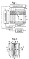
- the display in figures 1,2 comprises a liquid crystal cell 1 formed by a layer 2 of nematic or long pitch cholesteric liquid crystal material of negative dielectric anisotropy contained between glass walls 3, 4.
- a spacer ring 5 maintains the walls typically 1-6 ⁇ m apart. Additionally numerous beads of the same dimensions may be dispersed within the liquid crystal to maintain an accurate wall spacing.
- Strip like row electrodes 6 e.g. of SnO 2 or ITO are formed on one wall 3 and similar column electrodes 7 are formed on the other wall 4. With m-row and n-column electrodes this forms an m ⁇ n matrix of addressable elements or pixels. Each pixel is formed by the intersection of a row and column electrode.
- a row driver 8 supplies voltage to each row electrode 6.
- a column driver 9 supplies voltages to each column electrode 7.
- Control of applied voltages is from a control logic 10 which receives power from a voltage source 11 and timing from a clock 12.
- Either side of the cell 1 are polarisers 13, 14 arranged with their polarisation axis substantially crossed with respect to one another and substantially parallel to the alignment directions, if any, on the adjacent wall 3. 4 as described later. Additionally one or more compensation layers 19, 20 of e.g. stretched polymer are arranged between a cell wall under a polariser (if used) as described more fully later.
- a partly reflecting mirror 16 may be arranged behind the cell 1 together with a light source 15. These allow the display to be seen in reflection and lit from behind in dull ambient lighting. For a transmission device, the mirror may be omitted.
- one of the cell walls 3, 4 Prior to assembly, one of the cell walls 3, 4 has formed thereon a grating layer 17 which is treated eg by lecithin to give a homeotropic orientation.
- the other surface is treated to give a substantially planar surface with a preferred alignment direction, eg a rubbed layer 18 of P1-32 (Ciba Geigy) or a polyimide.
- a rubbed layer 18 of P1-32 (Ciba Geigy) or a polyimide This provides a tilted homogeneous alignment treatment in which the surface tilt (or pretilt) is typically 2-15°.
- the grating may be a profiled layer of a photopolymer formed by a photolithographic process e.g. M C Hutley, Diffraction Gratings (Academic Press. London 1982) p 95-125; and F Horn. Physics World. 33 (March 1993).
- the bigrating may be formed by embossing; M T Gale. J Kane and K Knop. J App. Photo Eng. 4, 2, 41 (1978), or ruling; E G Loewen and R S Wiley. Proc SPIE, 88 (1987), or by transfer from a carrier layer.
- the grating may be produced as described in PCT/GB97/01019.
- the grating on wall 3 was fabricated into Shipley 1805 photoresist by contact photolithography using a chrome on glass mask with a pitch of 1 ⁇ m (0.5 ⁇ m lines. 0.5 ⁇ m gaps). Adjustment of the exposure time allowed different groove depths to be obtained. In this case a mercury lamp source was used with an intensity of 0.5mW/cm 2 . Development was carried out in Shipley MF319 for 10 seconds followed by a water rinse. Finally the grating was exposed to deep UV and baked at 160°C to ensure insolubility in the liquid crystal. Prior to cell construction. the grating surface was treated with a lecithin solution in order to induce a homeotropic surface.
- nematic material which may be e.g. EN38 (Chisso) or ZLI-4788 (Merck).
- the bottom surface is the alignment layer 18 on wall 4 (not shown) which induces a pretilted planar alignment (in the x direction) while the upper surface is a grating layer 17 on wall 3 (not shown) surface coated with a surfactant to induce a homeotropic orientation.
- the grating grooves point in the y direction.
- N ( ⁇ nd / ⁇ ) 2 + 0.25 where ⁇ n is the nematic birefringence, d is the cell gap and ⁇ is the operating wavelength.
- a normally black mode can be obtained by using parallel polarisers along either the x or y direction.
- the optical contrast is obtained using voltages between V 1 and V 2 .
- the nematic director is substantially planar and so the black and white states as well as intermediate grey levels are obtained with improved and symmetric viewing angle characteristics.
- Variation of the grating groove depth influences the voltage at which the transition to a twisted state occurs. A higher transition voltage ensures a fully planar structure.
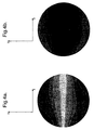
- Figure 4b shows the transmission of the dark state (zero volts) for this configuration.
- the contours starting with the darkest region correspond to the normalised transmission between crossed polarisers in the ranges:
- the highest transmission is 0.5 as the first polariser absorbs half the incident radiation.
- Figure 5 shows a schematic of a modified configuration in which a 3 ⁇ m positive uniaxial compensator layer 19 between walls 18, 21 is adjacent to the alignment layer 18; eg a layer from Nitto Denko Japan in their NRF series.
- the compensator layer 19 has an optical axis along z and has the same birefringence as the liquid crystal material 2.
- Polariser 13 has its optical axis along the x-axis, whilst the polariser 14 has its optical axis along the y-axis.
- Figure 6a shows the dark (zero volts) transmission which still has regions in the 0.35 - 0.40 range but has a larger region in the range 0.00 - 0.05 which compared to figure 4a. This leads to a larger viewing region with a contrast ratio greater than 10:1 as shown in figure 6b.
- Figure 7 shows another example where a 2 ⁇ m positive uniaxial compensator layer 20 has been added adjacent to the grating layer 17.
- the compensator layer 19 has an optical axis tilted at 45° to z in the x-z plane (tilt direction as shown) and has the same birefringence as the liquid crystal.
- Figure 8a shows the dark state (zero volts) transmission which shows that a large portion of the viewing cone now lies in the 0.0 - 0.05 range.
- the isocontrast plot (figure 8b) shows a >10:1 region that extends from -37.5° to +27.8° which is larger than the uncompensated case. The contrast is also high in two of the diagonal viewing directions.
- birefringent compensator layers 19, 20 are arranged adjacent the alignment layer 18 and the grating layer 17 as shown in figure 9.
- the compensator 19 is a 3 ⁇ m thick positive uniaxial layer with its optical axis in the z direction.
- the compensator 20 is a 4 ⁇ m thick positive uniaxial layer with its optical axis in the x direction. Both layers 19, 20 have the same birefringence as the liquid crystal material 2.
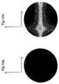
- Figure 10a shows the transmission in the dark (zero volts) state.
- the region in the range of 0.0 - 0.05 is larger than the uncompensated case and figure 10b shows that the contrast extends across a wider region.
- one birefringent compensator layer 20 is arranged adjacent the grating layer 17 and has an optic axis which varies through the thickness of the layer as shown in figure 11.
- the axis tilts from 0° to 90° in such a way that tilt is proportional to z position.
- the layer thickness is 5 ⁇ m and the material has the same optical birefringence as the liquid crystal material 2.
- Figure 12a shows that the dark state transmission of 0.0 - 0.05 extends in a large cross shaped region from -60° to +60° in both the x and y directions.
- the isocontrast plot shows that the region of>10:1 also extends to ⁇ 60° in both directions. Hence this type of compensation has lead to significant improvement.
- a birefringent compensator layer 20 is arranged adjacent the grating layer 17 and is a 5 ⁇ m negative uniaxial layer with its optic axis represented by the arrows in figure 13. This axis tilts from 0° to 90° through the thickness of the layer in a linear manner.
- the birefringence of this compensator layer 20 has the same value as the liquid crystal 2 but is opposite in sign.
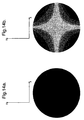
- Figure 14a shows an excellent dark state with the majority of the viewing cone having a transmission less than 0.05.
- the viewing characteristics also show very good symmetry.
- the corresponding isocontrast plot (figure 14b) shows a very high contrast of >100:1 extending from -60° to +60° in both the x and y directions.
- the viewing is also good in the diagonal directions with the contrast ratio remaining greater than 10:1 as far as 43° in all quadrants.
- a biaxial compensator layer 20 adjacent the grating 1.7 has been used for compensation: eg a layer from Nitto Denko Japan in their NFZ series.
- the dark state transmission (figure 16a) is not as good as example 5 but the 0.0 - 0.05 contour is still improved in some regions compared to the uncompensated case.
- the isocontrast plot (figure 16b) also shows a wider region of high contrast in the negative x direction compared to the uncompensated case.
- the viewing characteristics of the VCT mode can be improved by adding one or more birefringence layers. These layers compensate the variation in transmission which occurs when the VCT is viewed from different incident and azimuthal angles. In these cases the worst case VCT has been chosen. In many cases the uncompensated VCT can have much better viewing (see GB97/01019) but at the expense of higher voltage operation. Compensation of an intermediate voltage VCT will lead to even better viewing characteristics than those shown in the above examples. This is because the nematic director can achieve a lower average tilt through the thickness of the cell before the twist threshold occurs.
- the compensation layers can be made from a wide variety of materials.
- ⁇ n nematic birefringence
- d liquid crystal layer thickness
- ⁇ n.d liquid crystal layer thickness
- ⁇ n.d liquid crystal layer thickness
- the various compensator layer materials can be used singly or in any suitable combination on either side of the cell.
Landscapes
- Physics & Mathematics (AREA)
- Nonlinear Science (AREA)
- Chemical & Material Sciences (AREA)
- Crystallography & Structural Chemistry (AREA)
- General Physics & Mathematics (AREA)
- Optics & Photonics (AREA)
- Liquid Crystal (AREA)
Claims (16)
- Dispositif à cristaux liquides VCT comprenant :dans lequelun matériau cristal liquide nématique ou nématique chiral (2) d'anisotropie diélectrique négative ;deux parois contenant des cellules (3, 4) écartées l'une de l'autre et portant des électrodes (6, 7) ou un autre moyen pour appliquer un champ à la couche de cristaux liquides (2) ;une surface d'alignement (18) sur une paroi de cellule (4) assurant un alignement bien plan du cristal liquide avec une direction définie d'alignement azimutal ;une surface d'alignement (17) sur la seconde paroi de cellule (3) assurant un alignement bien homéotrope (z) du matériau cristal liquide adjacent et qui fournit également une direction définie d'alignement azimutal (y) au cristal liquide adjacent lorsque ledit cristal liquide proche de la seconde paroi de cellule (3) s'écarte de façon significative dudit alignement bien homéotrope ;des moyens (13, 14) pour faire la distinction entre deux états optiques différents ;
une ou plusieurs couches de compensateur biréfringentes (19, 20) sont disposées de façon adjacente à une ou aux deux parois de cellule (3, 4) de façon à améliorer les caractéristiques de vision de l'écran. - Dispositif selon la revendication 1, dans lequel le retard d'une couche de compensateur (19, 20) est en grande partie le même que celui du matériau de cristal liquide (2).
- Dispositif selon la revendication 1, dans lequel le retard d'une couche de compensateur (19, 20) est inférieur à celui du matériau de cristal liquide (2).
- Dispositif selon la revendication 1, dans lequel le retard d'une couche de compensateur (19, 20) est supérieur à celui du matériau de cristal liquide (2).
- Dispositif selon la revendication 1, dans lequel le retard d'une couche de compensateur (19, 20) se situe dans l'intervalle 0,05µm < Δn.d < 5 µm.
- Dispositif selon la revendication 1, dans lequel l'alignement sur la seconde paroi de cellule (3) est une structure de grille (17) recouverte d'un matériau d'alignement homéotrope, et une couche de compensateur (19, 20) est disposée de façon adjacente à la seconde paroi de cellule (3).
- Dispositif selon la revendication 1, dans lequel l'alignement sur la première paroi de cellule (4) est une couche de polymère en ruban (18), et une couche de compensateur (19, 20) est disposée de façon adjacente à la première paroi de cellule (4).
- Dispositif selon la revendication 1, dans lequel deux couches de compensateur (19, 20) sont l'une et l'autre disposées de façon adjacente à chaque paroi de cellule (3, 4), et les couches de compensateur (19, 20) sont de construction identique.
- Dispositif selon la revendication 1, dans lequel deux couches de compensateur (19, 20) sont l'une et l'autre disposées de façon adjacente à chaque paroi de cellule (3, 4), et les couches de compensateur (19, 20) sont de construction différente.
- Dispositif selon la revendication 1, dans lequel une couche de compensateur biréfringente (19, 20) est une couche de polymère.
- Dispositif selon la revendication 1, dans lequel une couche de compensateur biréfringente (19, 20) est une couche de matériau cristal liquide.
- Dispositif selon la revendication 1, dans lequel une couche de compensateur biréfringente (19, 20) est une couche de matériau cristal liquide contenu entre des parois de cellule dont la surface est traitée pour aligner le matériau cristal liquide.
- Dispositif selon la revendication 1, dans lequel une couche de compensateur biréfringente (19, 20) est une couche de matériau cristal liquide contenu entre des parois de cellule dont la surface est traitée pour aligner le matériau cristal liquide et est munie de structures d'électrodes pour appliquer un champ électrique au matériau cristal liquide.
- Dispositif selon la revendication 1, dans lequel une couche de compensateur biréfringente (19, 20) est une couche de matériau polymère cristal liquide aligné.
- Dispositif selon la revendication 1, dans lequel une couche de compensateur biréfringente (19, 20) est une couche de quartz ou de calcite.
- Dispositif selon la revendication 1, dans lequel une couche de compensateur biréfringente (19, 20) est une couche de matériau évaporé obliquement.
Applications Claiming Priority (3)
| Application Number | Priority Date | Filing Date | Title |
|---|---|---|---|
| GBGB9713164.3A GB9713164D0 (en) | 1997-06-23 | 1997-06-23 | Liquid crystal device |
| GB9713164 | 1997-06-23 | ||
| PCT/GB1998/001812 WO1998059275A1 (fr) | 1997-06-23 | 1998-06-19 | Dispositif a cristaux liquides |
Publications (2)
| Publication Number | Publication Date |
|---|---|
| EP0991977A1 EP0991977A1 (fr) | 2000-04-12 |
| EP0991977B1 true EP0991977B1 (fr) | 2002-05-15 |
Family
ID=10814745
Family Applications (1)
| Application Number | Title | Priority Date | Filing Date |
|---|---|---|---|
| EP98930912A Expired - Lifetime EP0991977B1 (fr) | 1997-06-23 | 1998-06-19 | Dispositif a cristaux liquides |
Country Status (7)
| Country | Link |
|---|---|
| US (1) | US6577363B1 (fr) |
| EP (1) | EP0991977B1 (fr) |
| JP (1) | JP2002506532A (fr) |
| DE (1) | DE69805411T2 (fr) |
| GB (1) | GB9713164D0 (fr) |
| MY (1) | MY132997A (fr) |
| WO (1) | WO1998059275A1 (fr) |
Families Citing this family (3)
| Publication number | Priority date | Publication date | Assignee | Title |
|---|---|---|---|---|
| EP1028346A3 (fr) | 1999-02-12 | 2002-05-02 | Matsushita Electric Industrial Co., Ltd. | Elément à cristaux liquides et son procédé de fabrication |
| GB9928126D0 (en) | 1999-11-30 | 2000-01-26 | Secr Defence | Bistable nematic liquid crystal device |
| KR100344185B1 (ko) * | 2000-06-13 | 2002-07-20 | 주식회사 네오텍리서치 | 액정표시장치 |
Family Cites Families (5)
| Publication number | Priority date | Publication date | Assignee | Title |
|---|---|---|---|---|
| US5380459A (en) * | 1990-04-20 | 1995-01-10 | Ricoh Company, Ltd. | Liquid crystal display device with improved viewing angle dependence of color |
| JPH0498223A (ja) * | 1990-08-17 | 1992-03-30 | Nec Corp | 液晶素子 |
| WO1996010774A1 (fr) * | 1994-09-30 | 1996-04-11 | Rockwell International Corporation | Amelioration de l'angle de vision pour afficheurs a cristaux liquides cholesteriques a alignement vertical |
| GB9521106D0 (en) | 1995-10-16 | 1995-12-20 | Secr Defence | Bistable nematic liquid crystal device |
| GB9607854D0 (en) | 1996-04-16 | 1996-06-19 | Secr Defence | Liquid crystal device |
-
1997
- 1997-06-23 GB GBGB9713164.3A patent/GB9713164D0/en not_active Ceased
-
1998
- 1998-06-19 JP JP50400299A patent/JP2002506532A/ja active Pending
- 1998-06-19 EP EP98930912A patent/EP0991977B1/fr not_active Expired - Lifetime
- 1998-06-19 US US09/381,505 patent/US6577363B1/en not_active Expired - Fee Related
- 1998-06-19 DE DE69805411T patent/DE69805411T2/de not_active Expired - Lifetime
- 1998-06-19 WO PCT/GB1998/001812 patent/WO1998059275A1/fr not_active Ceased
- 1998-06-22 MY MYPI98002829A patent/MY132997A/en unknown
Also Published As
| Publication number | Publication date |
|---|---|
| WO1998059275A1 (fr) | 1998-12-30 |
| EP0991977A1 (fr) | 2000-04-12 |
| US6577363B1 (en) | 2003-06-10 |
| DE69805411T2 (de) | 2002-11-21 |
| DE69805411D1 (de) | 2002-06-20 |
| JP2002506532A (ja) | 2002-02-26 |
| MY132997A (en) | 2007-10-31 |
| GB9713164D0 (en) | 1997-08-27 |
Similar Documents
| Publication | Publication Date | Title |
|---|---|---|
| US6341002B1 (en) | Liquid crystal display device | |
| JP3321558B2 (ja) | 液晶表示装置用の楕円偏光板 | |
| US5619356A (en) | Reflective liquid crystal display device having a compensator with a retardation value between 0.15 μm and 0.38 μm and a single polarizer | |
| KR100239266B1 (ko) | 액정표시장치 및 그의 위상지연 보상방법 | |
| EP0816906B1 (fr) | Dispositifs à cristal liquide | |
| EP0576931B1 (fr) | Dispositif d'affichage à cristal liquide | |
| EP1459128B1 (fr) | Dispositif d'affichage a cristaux liquides transflectif | |
| US5184236A (en) | Twisted nematic liquid crystal display device with retardation plates having phase axis direction within 15° of alignment direction | |
| EP0616240B1 (fr) | Affichage et dispositif à cristal liquide | |
| US6078370A (en) | Method of constructing an array of pixels for use in a multi-pixel liquid crystal display | |
| EP0894285B1 (fr) | Dispositif a cristaux liquides | |
| US5568287A (en) | Liquid crystal device with optical means of high refractive index at pixels and low refractive index between pixels | |
| US4904058A (en) | Liquid crystal display panel | |
| KR100722458B1 (ko) | 액정표시소자 | |
| KR100695698B1 (ko) | 디스플레이 디바이스, 보상 필름 및 액정 디스플레이 | |
| US5726729A (en) | Liquid crystal display device | |
| KR0177049B1 (ko) | 액정표시장치 | |
| EP0991977B1 (fr) | Dispositif a cristaux liquides | |
| GB2371372A (en) | Liquid Crystal Device | |
| JPH06235914A (ja) | 液晶表示装置 | |
| JP3619506B2 (ja) | 液晶表示装置 | |
| KR19990037025A (ko) | 액정 표시 장치 | |
| JPH09222601A (ja) | 液晶表示素子および光学異方素子 | |
| KR100632215B1 (ko) | 반투과형 액정표시장치 | |
| KR101688593B1 (ko) | 횡전계 모드 반사투과형 액정표시장치 |
Legal Events
| Date | Code | Title | Description |
|---|---|---|---|
| PUAI | Public reference made under article 153(3) epc to a published international application that has entered the european phase |
Free format text: ORIGINAL CODE: 0009012 |
|
| 17P | Request for examination filed |
Effective date: 19990916 |
|
| AK | Designated contracting states |
Kind code of ref document: A1 Designated state(s): DE FR GB |
|
| GRAG | Despatch of communication of intention to grant |
Free format text: ORIGINAL CODE: EPIDOS AGRA |
|
| RAP1 | Party data changed (applicant data changed or rights of an application transferred) |
Owner name: QINETIQ LIMITED |
|
| 17Q | First examination report despatched |
Effective date: 20010907 |
|
| GRAG | Despatch of communication of intention to grant |
Free format text: ORIGINAL CODE: EPIDOS AGRA |
|
| GRAH | Despatch of communication of intention to grant a patent |
Free format text: ORIGINAL CODE: EPIDOS IGRA |
|
| RBV | Designated contracting states (corrected) |
Designated state(s): DE FR GB |
|
| GRAH | Despatch of communication of intention to grant a patent |
Free format text: ORIGINAL CODE: EPIDOS IGRA |
|
| GRAA | (expected) grant |
Free format text: ORIGINAL CODE: 0009210 |
|
| AK | Designated contracting states |
Kind code of ref document: B1 Designated state(s): DE FR GB |
|
| REG | Reference to a national code |
Ref country code: GB Ref legal event code: FG4D |
|
| REF | Corresponds to: |
Ref document number: 69805411 Country of ref document: DE Date of ref document: 20020620 |
|
| ET | Fr: translation filed | ||
| PLBE | No opposition filed within time limit |
Free format text: ORIGINAL CODE: 0009261 |
|
| STAA | Information on the status of an ep patent application or granted ep patent |
Free format text: STATUS: NO OPPOSITION FILED WITHIN TIME LIMIT |
|
| 26N | No opposition filed |
Effective date: 20030218 |
|
| PGFP | Annual fee paid to national office [announced via postgrant information from national office to epo] |
Ref country code: FR Payment date: 20121130 Year of fee payment: 15 Ref country code: DE Payment date: 20121121 Year of fee payment: 15 |
|
| PGFP | Annual fee paid to national office [announced via postgrant information from national office to epo] |
Ref country code: GB Payment date: 20121120 Year of fee payment: 15 |
|
| GBPC | Gb: european patent ceased through non-payment of renewal fee |
Effective date: 20130619 |
|
| REG | Reference to a national code |
Ref country code: FR Ref legal event code: ST Effective date: 20140228 |
|
| REG | Reference to a national code |
Ref country code: DE Ref legal event code: R119 Ref document number: 69805411 Country of ref document: DE Effective date: 20140101 |
|
| PG25 | Lapsed in a contracting state [announced via postgrant information from national office to epo] |
Ref country code: DE Free format text: LAPSE BECAUSE OF NON-PAYMENT OF DUE FEES Effective date: 20140101 Ref country code: GB Free format text: LAPSE BECAUSE OF NON-PAYMENT OF DUE FEES Effective date: 20130619 |
|
| PG25 | Lapsed in a contracting state [announced via postgrant information from national office to epo] |
Ref country code: FR Free format text: LAPSE BECAUSE OF NON-PAYMENT OF DUE FEES Effective date: 20130701 |