EP0992837B1 - Reflektierende Halbleitervorrichtung - Google Patents
Reflektierende Halbleitervorrichtung Download PDFInfo
- Publication number
- EP0992837B1 EP0992837B1 EP99118795A EP99118795A EP0992837B1 EP 0992837 B1 EP0992837 B1 EP 0992837B1 EP 99118795 A EP99118795 A EP 99118795A EP 99118795 A EP99118795 A EP 99118795A EP 0992837 B1 EP0992837 B1 EP 0992837B1
- Authority
- EP
- European Patent Office
- Prior art keywords
- reflection type
- display device
- liquid crystal
- type display
- optical fiber
- Prior art date
- Legal status (The legal status is an assumption and is not a legal conclusion. Google has not performed a legal analysis and makes no representation as to the accuracy of the status listed.)
- Expired - Lifetime
Links
- 239000004065 semiconductor Substances 0.000 title description 24
- 239000013307 optical fiber Substances 0.000 claims description 81
- 239000004973 liquid crystal related substance Substances 0.000 claims description 74
- 239000000758 substrate Substances 0.000 claims description 34
- 230000001413 cellular effect Effects 0.000 claims description 4
- 239000010409 thin film Substances 0.000 claims description 2
- 230000005540 biological transmission Effects 0.000 description 10
- 239000011347 resin Substances 0.000 description 6
- 229920005989 resin Polymers 0.000 description 6
- 239000011248 coating agent Substances 0.000 description 4
- 238000000576 coating method Methods 0.000 description 4
- 239000012779 reinforcing material Substances 0.000 description 3
- 238000003491 array Methods 0.000 description 2
- 239000010408 film Substances 0.000 description 2
- 230000008878 coupling Effects 0.000 description 1
- 238000010168 coupling process Methods 0.000 description 1
- 238000005859 coupling reaction Methods 0.000 description 1
- 238000005516 engineering process Methods 0.000 description 1
- 239000000835 fiber Substances 0.000 description 1
- 238000005286 illumination Methods 0.000 description 1
- 230000010365 information processing Effects 0.000 description 1
- 238000004519 manufacturing process Methods 0.000 description 1
- 238000000034 method Methods 0.000 description 1
- 238000004088 simulation Methods 0.000 description 1
- 239000013589 supplement Substances 0.000 description 1
Images


Classifications
-
- G—PHYSICS
- G02—OPTICS
- G02B—OPTICAL ELEMENTS, SYSTEMS OR APPARATUS
- G02B6/00—Light guides; Structural details of arrangements comprising light guides and other optical elements, e.g. couplings
- G02B6/0001—Light guides; Structural details of arrangements comprising light guides and other optical elements, e.g. couplings specially adapted for lighting devices or systems
- G02B6/0011—Light guides; Structural details of arrangements comprising light guides and other optical elements, e.g. couplings specially adapted for lighting devices or systems the light guides being planar or of plate-like form
- G02B6/0013—Means for improving the coupling-in of light from the light source into the light guide
- G02B6/0023—Means for improving the coupling-in of light from the light source into the light guide provided by one optical element, or plurality thereof, placed between the light guide and the light source, or around the light source
- G02B6/0028—Light guide, e.g. taper
-
- G—PHYSICS
- G02—OPTICS
- G02B—OPTICAL ELEMENTS, SYSTEMS OR APPARATUS
- G02B6/00—Light guides; Structural details of arrangements comprising light guides and other optical elements, e.g. couplings
- G02B6/0001—Light guides; Structural details of arrangements comprising light guides and other optical elements, e.g. couplings specially adapted for lighting devices or systems
- G02B6/0005—Light guides; Structural details of arrangements comprising light guides and other optical elements, e.g. couplings specially adapted for lighting devices or systems the light guides being of the fibre type
- G02B6/0008—Light guides; Structural details of arrangements comprising light guides and other optical elements, e.g. couplings specially adapted for lighting devices or systems the light guides being of the fibre type the light being emitted at the end of the fibre
-
- G—PHYSICS
- G02—OPTICS
- G02B—OPTICAL ELEMENTS, SYSTEMS OR APPARATUS
- G02B6/00—Light guides; Structural details of arrangements comprising light guides and other optical elements, e.g. couplings
- G02B6/0001—Light guides; Structural details of arrangements comprising light guides and other optical elements, e.g. couplings specially adapted for lighting devices or systems
- G02B6/0011—Light guides; Structural details of arrangements comprising light guides and other optical elements, e.g. couplings specially adapted for lighting devices or systems the light guides being planar or of plate-like form
- G02B6/0033—Means for improving the coupling-out of light from the light guide
- G02B6/0035—Means for improving the coupling-out of light from the light guide provided on the surface of the light guide or in the bulk of it
- G02B6/0038—Linear indentations or grooves, e.g. arc-shaped grooves or meandering grooves, extending over the full length or width of the light guide
-
- G—PHYSICS
- G02—OPTICS
- G02B—OPTICAL ELEMENTS, SYSTEMS OR APPARATUS
- G02B6/00—Light guides; Structural details of arrangements comprising light guides and other optical elements, e.g. couplings
- G02B6/0001—Light guides; Structural details of arrangements comprising light guides and other optical elements, e.g. couplings specially adapted for lighting devices or systems
- G02B6/0011—Light guides; Structural details of arrangements comprising light guides and other optical elements, e.g. couplings specially adapted for lighting devices or systems the light guides being planar or of plate-like form
- G02B6/0066—Light guides; Structural details of arrangements comprising light guides and other optical elements, e.g. couplings specially adapted for lighting devices or systems the light guides being planar or of plate-like form characterised by the light source being coupled to the light guide
- G02B6/0068—Arrangements of plural sources, e.g. multi-colour light sources
-
- G—PHYSICS
- G02—OPTICS
- G02F—OPTICAL DEVICES OR ARRANGEMENTS FOR THE CONTROL OF LIGHT BY MODIFICATION OF THE OPTICAL PROPERTIES OF THE MEDIA OF THE ELEMENTS INVOLVED THEREIN; NON-LINEAR OPTICS; FREQUENCY-CHANGING OF LIGHT; OPTICAL LOGIC ELEMENTS; OPTICAL ANALOGUE/DIGITAL CONVERTERS
- G02F1/00—Devices or arrangements for the control of the intensity, colour, phase, polarisation or direction of light arriving from an independent light source, e.g. switching, gating or modulating; Non-linear optics
- G02F1/01—Devices or arrangements for the control of the intensity, colour, phase, polarisation or direction of light arriving from an independent light source, e.g. switching, gating or modulating; Non-linear optics for the control of the intensity, phase, polarisation or colour
- G02F1/13—Devices or arrangements for the control of the intensity, colour, phase, polarisation or direction of light arriving from an independent light source, e.g. switching, gating or modulating; Non-linear optics for the control of the intensity, phase, polarisation or colour based on liquid crystals, e.g. single liquid crystal display cells
- G02F1/133—Constructional arrangements; Operation of liquid crystal cells; Circuit arrangements
- G02F1/1333—Constructional arrangements; Manufacturing methods
- G02F1/1335—Structural association of cells with optical devices, e.g. polarisers or reflectors
- G02F1/133553—Reflecting elements
-
- G—PHYSICS
- G02—OPTICS
- G02F—OPTICAL DEVICES OR ARRANGEMENTS FOR THE CONTROL OF LIGHT BY MODIFICATION OF THE OPTICAL PROPERTIES OF THE MEDIA OF THE ELEMENTS INVOLVED THEREIN; NON-LINEAR OPTICS; FREQUENCY-CHANGING OF LIGHT; OPTICAL LOGIC ELEMENTS; OPTICAL ANALOGUE/DIGITAL CONVERTERS
- G02F1/00—Devices or arrangements for the control of the intensity, colour, phase, polarisation or direction of light arriving from an independent light source, e.g. switching, gating or modulating; Non-linear optics
- G02F1/01—Devices or arrangements for the control of the intensity, colour, phase, polarisation or direction of light arriving from an independent light source, e.g. switching, gating or modulating; Non-linear optics for the control of the intensity, phase, polarisation or colour
- G02F1/13—Devices or arrangements for the control of the intensity, colour, phase, polarisation or direction of light arriving from an independent light source, e.g. switching, gating or modulating; Non-linear optics for the control of the intensity, phase, polarisation or colour based on liquid crystals, e.g. single liquid crystal display cells
- G02F1/133—Constructional arrangements; Operation of liquid crystal cells; Circuit arrangements
- G02F1/1333—Constructional arrangements; Manufacturing methods
- G02F1/1335—Structural association of cells with optical devices, e.g. polarisers or reflectors
- G02F1/1336—Illuminating devices
- G02F1/133615—Edge-illuminating devices, i.e. illuminating from the side
-
- G—PHYSICS
- G02—OPTICS
- G02F—OPTICAL DEVICES OR ARRANGEMENTS FOR THE CONTROL OF LIGHT BY MODIFICATION OF THE OPTICAL PROPERTIES OF THE MEDIA OF THE ELEMENTS INVOLVED THEREIN; NON-LINEAR OPTICS; FREQUENCY-CHANGING OF LIGHT; OPTICAL LOGIC ELEMENTS; OPTICAL ANALOGUE/DIGITAL CONVERTERS
- G02F1/00—Devices or arrangements for the control of the intensity, colour, phase, polarisation or direction of light arriving from an independent light source, e.g. switching, gating or modulating; Non-linear optics
- G02F1/01—Devices or arrangements for the control of the intensity, colour, phase, polarisation or direction of light arriving from an independent light source, e.g. switching, gating or modulating; Non-linear optics for the control of the intensity, phase, polarisation or colour
- G02F1/13—Devices or arrangements for the control of the intensity, colour, phase, polarisation or direction of light arriving from an independent light source, e.g. switching, gating or modulating; Non-linear optics for the control of the intensity, phase, polarisation or colour based on liquid crystals, e.g. single liquid crystal display cells
- G02F1/133—Constructional arrangements; Operation of liquid crystal cells; Circuit arrangements
- G02F1/1333—Constructional arrangements; Manufacturing methods
- G02F1/1335—Structural association of cells with optical devices, e.g. polarisers or reflectors
- G02F1/133524—Light-guides, e.g. fibre-optic bundles, louvered or jalousie light-guides
-
- G—PHYSICS
- G02—OPTICS
- G02F—OPTICAL DEVICES OR ARRANGEMENTS FOR THE CONTROL OF LIGHT BY MODIFICATION OF THE OPTICAL PROPERTIES OF THE MEDIA OF THE ELEMENTS INVOLVED THEREIN; NON-LINEAR OPTICS; FREQUENCY-CHANGING OF LIGHT; OPTICAL LOGIC ELEMENTS; OPTICAL ANALOGUE/DIGITAL CONVERTERS
- G02F1/00—Devices or arrangements for the control of the intensity, colour, phase, polarisation or direction of light arriving from an independent light source, e.g. switching, gating or modulating; Non-linear optics
- G02F1/01—Devices or arrangements for the control of the intensity, colour, phase, polarisation or direction of light arriving from an independent light source, e.g. switching, gating or modulating; Non-linear optics for the control of the intensity, phase, polarisation or colour
- G02F1/13—Devices or arrangements for the control of the intensity, colour, phase, polarisation or direction of light arriving from an independent light source, e.g. switching, gating or modulating; Non-linear optics for the control of the intensity, phase, polarisation or colour based on liquid crystals, e.g. single liquid crystal display cells
- G02F1/133—Constructional arrangements; Operation of liquid crystal cells; Circuit arrangements
- G02F1/1333—Constructional arrangements; Manufacturing methods
- G02F1/1335—Structural association of cells with optical devices, e.g. polarisers or reflectors
- G02F1/1336—Illuminating devices
- G02F1/133602—Direct backlight
- G02F1/133603—Direct backlight with LEDs
-
- G—PHYSICS
- G02—OPTICS
- G02F—OPTICAL DEVICES OR ARRANGEMENTS FOR THE CONTROL OF LIGHT BY MODIFICATION OF THE OPTICAL PROPERTIES OF THE MEDIA OF THE ELEMENTS INVOLVED THEREIN; NON-LINEAR OPTICS; FREQUENCY-CHANGING OF LIGHT; OPTICAL LOGIC ELEMENTS; OPTICAL ANALOGUE/DIGITAL CONVERTERS
- G02F1/00—Devices or arrangements for the control of the intensity, colour, phase, polarisation or direction of light arriving from an independent light source, e.g. switching, gating or modulating; Non-linear optics
- G02F1/01—Devices or arrangements for the control of the intensity, colour, phase, polarisation or direction of light arriving from an independent light source, e.g. switching, gating or modulating; Non-linear optics for the control of the intensity, phase, polarisation or colour
- G02F1/13—Devices or arrangements for the control of the intensity, colour, phase, polarisation or direction of light arriving from an independent light source, e.g. switching, gating or modulating; Non-linear optics for the control of the intensity, phase, polarisation or colour based on liquid crystals, e.g. single liquid crystal display cells
- G02F1/133—Constructional arrangements; Operation of liquid crystal cells; Circuit arrangements
- G02F1/1333—Constructional arrangements; Manufacturing methods
- G02F1/1335—Structural association of cells with optical devices, e.g. polarisers or reflectors
- G02F1/1336—Illuminating devices
- G02F1/133616—Front illuminating devices
-
- G—PHYSICS
- G02—OPTICS
- G02F—OPTICAL DEVICES OR ARRANGEMENTS FOR THE CONTROL OF LIGHT BY MODIFICATION OF THE OPTICAL PROPERTIES OF THE MEDIA OF THE ELEMENTS INVOLVED THEREIN; NON-LINEAR OPTICS; FREQUENCY-CHANGING OF LIGHT; OPTICAL LOGIC ELEMENTS; OPTICAL ANALOGUE/DIGITAL CONVERTERS
- G02F1/00—Devices or arrangements for the control of the intensity, colour, phase, polarisation or direction of light arriving from an independent light source, e.g. switching, gating or modulating; Non-linear optics
- G02F1/01—Devices or arrangements for the control of the intensity, colour, phase, polarisation or direction of light arriving from an independent light source, e.g. switching, gating or modulating; Non-linear optics for the control of the intensity, phase, polarisation or colour
- G02F1/13—Devices or arrangements for the control of the intensity, colour, phase, polarisation or direction of light arriving from an independent light source, e.g. switching, gating or modulating; Non-linear optics for the control of the intensity, phase, polarisation or colour based on liquid crystals, e.g. single liquid crystal display cells
- G02F1/133—Constructional arrangements; Operation of liquid crystal cells; Circuit arrangements
- G02F1/1333—Constructional arrangements; Manufacturing methods
- G02F1/1335—Structural association of cells with optical devices, e.g. polarisers or reflectors
- G02F1/1336—Illuminating devices
- G02F1/133618—Illuminating devices for ambient light
-
- G—PHYSICS
- G02—OPTICS
- G02F—OPTICAL DEVICES OR ARRANGEMENTS FOR THE CONTROL OF LIGHT BY MODIFICATION OF THE OPTICAL PROPERTIES OF THE MEDIA OF THE ELEMENTS INVOLVED THEREIN; NON-LINEAR OPTICS; FREQUENCY-CHANGING OF LIGHT; OPTICAL LOGIC ELEMENTS; OPTICAL ANALOGUE/DIGITAL CONVERTERS
- G02F1/00—Devices or arrangements for the control of the intensity, colour, phase, polarisation or direction of light arriving from an independent light source, e.g. switching, gating or modulating; Non-linear optics
- G02F1/01—Devices or arrangements for the control of the intensity, colour, phase, polarisation or direction of light arriving from an independent light source, e.g. switching, gating or modulating; Non-linear optics for the control of the intensity, phase, polarisation or colour
- G02F1/13—Devices or arrangements for the control of the intensity, colour, phase, polarisation or direction of light arriving from an independent light source, e.g. switching, gating or modulating; Non-linear optics for the control of the intensity, phase, polarisation or colour based on liquid crystals, e.g. single liquid crystal display cells
- G02F1/133—Constructional arrangements; Operation of liquid crystal cells; Circuit arrangements
- G02F1/1333—Constructional arrangements; Manufacturing methods
- G02F1/1335—Structural association of cells with optical devices, e.g. polarisers or reflectors
- G02F1/1336—Illuminating devices
- G02F1/133626—Illuminating devices providing two modes of illumination, e.g. day-night
-
- G—PHYSICS
- G02—OPTICS
- G02F—OPTICAL DEVICES OR ARRANGEMENTS FOR THE CONTROL OF LIGHT BY MODIFICATION OF THE OPTICAL PROPERTIES OF THE MEDIA OF THE ELEMENTS INVOLVED THEREIN; NON-LINEAR OPTICS; FREQUENCY-CHANGING OF LIGHT; OPTICAL LOGIC ELEMENTS; OPTICAL ANALOGUE/DIGITAL CONVERTERS
- G02F1/00—Devices or arrangements for the control of the intensity, colour, phase, polarisation or direction of light arriving from an independent light source, e.g. switching, gating or modulating; Non-linear optics
- G02F1/01—Devices or arrangements for the control of the intensity, colour, phase, polarisation or direction of light arriving from an independent light source, e.g. switching, gating or modulating; Non-linear optics for the control of the intensity, phase, polarisation or colour
- G02F1/13—Devices or arrangements for the control of the intensity, colour, phase, polarisation or direction of light arriving from an independent light source, e.g. switching, gating or modulating; Non-linear optics for the control of the intensity, phase, polarisation or colour based on liquid crystals, e.g. single liquid crystal display cells
- G02F1/133—Constructional arrangements; Operation of liquid crystal cells; Circuit arrangements
- G02F1/136—Liquid crystal cells structurally associated with a semi-conducting layer or substrate, e.g. cells forming part of an integrated circuit
- G02F1/1362—Active matrix addressed cells
Definitions
- the present invention relates to a reflection type semiconductor display device of a direct viewing type, and more particularly, to a reflection type liquid crystal display device (liquid crystal panel).
- the present invention also relates to a semiconductor device with a reflection type liquid crystal display device mounted thereon.
- a semiconductor device as referred to in the present invention may be, for example, information processing equipment such as a notebook-sized personal computer, a lap top type personal computer, an electronic notebook, or a mobile computer, a video camera, a digital still camera, a car navigation system, or a cellular telephone.
- information processing equipment such as a notebook-sized personal computer, a lap top type personal computer, an electronic notebook, or a mobile computer, a video camera, a digital still camera, a car navigation system, or a cellular telephone.
- notebook-sized PCs notebook-sized personal computers
- Liquid crystal panels fall into transmission type ones and reflection type ones.
- illumination light is transmitted through the liquid crystal panel from a back light provided at the back so that the user can visually confirm the display.
- a reflection type liquid crystal panel does not need a back light, and the display can be seen through reflection of external light on the liquid crystal panel.
- Such a back light consumes about 90% of power consumption of the transmission type liquid crystal panel, and thus, power consumption of a transmission type liquid crystal panel is large.
- a reflection type liquid crystal panel is inferior to that of a transmission type liquid crystal panel, power consumption of a reflection type liquid crystal panel is smaller than that of a transmission type liquid crystal panel, and thus, a reflection type liquid crystal panel is advantageous when used in a notebook-sized PC or a mobile PC.
- GB 2246231 discloses a device for back-lighting a liquid crystal display panel.
- JP 04029291 discloses a flexible light transmission plate having a uniform luminance by arranging many bubbles in the plate-shaped flexible light transmission plate main body, which is provided on a back side of a flexible liquid crystal panel. This disclosure therefore also addresses a back-lighting display device.
- DE 3314323 A1 discloses a reflection type display device. This device is, however, not a liquid crystal display device .
- EP-A-056843 discloses a reflective LCD with a light guide plate on a front side and liquid crystal between the bottom substrate and the light guide plate.
- EP-A-617310 discloses a reflection type liquid crystal display device using reflective electrodes.
- JP 9096760 discloses coupling of light into a fiber via microlenses.
- an object of the invention is to provide a reflection type semiconductor display device having high display quality level without insufficiency of the amount of light even when it is used indoors.
- light other than incident light on a liquid crystal panel is utilized as an auxiliary light source of a reflection type semiconductor display device.
- Fig. 1 shows a schematic structural view of a reflection type semiconductor display device using a reflection type liquid crystal panel according to the present invention.
- Reference numerals 101, 102, and 103 denote a main body, a reflection type liquid crystal panel, and an optical fiber array, respectively.
- the optical fiber array 103 includes a plurality of optical fiber cables 104.
- Each of the optical fiber cables 104 is a bundle of a plurality of optical fibers, examples thereof being shown in Figs. 2A and 2B .
- the optical fiber array is used as means for taking in external light.
- reference numeral 201 denotes an optical fiber, an enlargement thereof being shown at the lower portion in Figs. 2A and 2B .
- the optical fiber 201 has a core and a clad.
- the index of refraction of the core is larger than that of the clad, and light travels as it repeats total internal reflections at the interface between the core and the clad.
- a coating 202 is formed of a resin or the like.
- a reinforcing material 203 is formed of a resin or the like.
- the reinforcing material 203 fills the space among the optical fibers to improve the strength.
- Fig. 3 shows a sectional view of a reflection type liquid crystal panel according to the present invention.
- Reference numeral 301 denotes a substrate.
- Reference numerals 302 and 303 denote driver TFTs (thin film transistors).
- Reference numerals 304, 305, 306, and 307 denote a pixel TFT, a reflection electrode, liquid crystal, and a counter substrate, respectively.
- the pixel TFT can be made of amorphous semiconductor film or polycrystalline semiconductor film.
- a transparent electrode (not shown) is provided under the counter substrate.
- the optical fiber cables 104 are positioned such that light taken in from one end of each of the optical fiber cables 104 is emitted from the other end thereof to the counter substrate. Consequently, incident light entered into the optical fiber cables travels through the optical fibers, enters the counter substrate 307, traveling through the counter substrate 307, and then enters the liquid crystal.
- the upper surface of the counter substrate 307 is appropriately processed to allow incident light on the liquid crystal by eliminating the requirement for the total internal reflections of light traveling through the substrate at the interface.
- the processing condition can be most suitably set through simulation or the like.
- the upper surface of the counter substrate 307 is formed with patterns, but the present invention is not limited thereto.
- the panel may be structured to use a counter substrate used in a general reflection type liquid crystal panel and a light guide plate 408.
- Reference numeral 401 denotes a substrate.
- Reference numerals 402 and 403 denote driver TFTs.
- Reference numerals 404, 405, 406, and 407 denote a pixel TFT, a reflection electrode, liquid crystal, and a counter substrate, respectively.
- the upper surface of the light guide plate 408 is processed so as to eliminate the requirement for the total internal reflections of incident light traveling through the light guide plate 408 at the interface.
- any suitable means may be used to allow incident light taken in by the optical fiber cables 104 to travel through the counter substrate or the light guide plate into the liquid crystal.
- a reflection type display device in which light emitted from one end an optical fiber enters said reflection type display device, wherein the light is external light taken in from the other end of the optical fiber.
- a reflection type semiconductor display device in which light emitted from one end of an optical fiber enters a counter substrate of said reflection type semiconductor display device, wherein the light is external light taken in from the other end of the optical fiber.
- a reflection type semiconductor display device in which light emitted from one end of an optical fiber enters a light guide plate provided so as to oppose to said reflection type semiconductor display device, wherein the light is external light taken in from the other end of the optical fiber.
- a reflection type semiconductor display device in the foregoing structure further comprises a front ligh.t
- the above-described front light comprises an LED.
- the present embodiment is a case where a liquid crystal panel according to the present invention is mounted on a notebook-sized PC.
- FIG. 5 shows the appearance of the notebook-sized PC of the present embodiment.
- Reference numerals 501, 502, 503, 504, and 505 denote a main body, a keyboard, a pointing device, a reflection type liquid crystal panel, and an optical fiber array, respectively.
- the optical fiber array of the present embodiment has the optical fiber cables 104 as shown in Fig. 2A .
- Fig. 6 shows a sectional view of the reflection type liquid crystal panel 504 of the present embodiment.
- Reference numeral 601 denotes a substrate.
- Reference numerals 602 and 603 are driver TFTs.
- Reference numerals 604, 605, 606, and 607 denote a pixel TFT, a reflection electrode, liquid crystal, and a counter substrate, respectively. Dots 608 are formed on the counter substrate 607.
- the optical fiber cables 104 are positioned so as to emit light taken into the counter substrate. Incident light entered into the optical fiber cables enters the counter substrate 607, traveling through the counter substrate 607, and then enters the liquid crystal 606. It is to be noted that the dots 608 are formed on the upper surface of the counter substrate 607 to allow incident light on the liquid crystal by eliminating the requirement for the total internal reflections of light traveling through the substrate at the interface.
- the present embodiment is a case where the structure of the reflection type liquid crystal panel is modified in the notebook-sized PC described in Embodiment 1.
- Fig. 7 shows a sectional view of the reflection type liquid crystal panel.
- Reference numeral 701 denotes a substrate.
- Reference numerals 702 and 703 are driver TFTs.
- Reference numerals 704, 705, 706, 707, and 708 denote a pixel TFT, a reflection electrode, liquid crystal, a counter substrate, and a light guide plate, respectively. Dots 709 are formed on the light guide plate 708.
- light taken in the optical fiber cables 104 enters the light guide plate 708, traveling through the light guide plate 708, and then enters the liquid crystal 706.
- the present embodiment is a case where the optical fiber cables are modified which form the optical fiber array used in the liquid crystal panel described in Embodiment 1 or Embodiment 2 as means for solving the above-mentioned problem.
- the optical fiber array of the present embodiment is an aggregate of a plurality of optical fiber cables as shown in Fig. 8 .
- Each of the optical fiber cables 801 is a bundle of a plurality of optical fibers 802.
- a microlens array 803 is positioned at an aperture of each optical fiber cable 801 for taking in the optical fibers.
- a coating 804 is formed of a resin or the like.
- Fig. 9 illustrates the function of a microlens 803-1 forming the microlens array 803 of the present embodiment.
- the microlens array 803 is an aggregate of a plurality of microlenses 803-1.
- Fig. 9 shows one microlens 803-1 for conveniences' sake.
- the size of the microlens 803-1 substantially equals to that of the clad of the optical fiber 802.
- the microlens 803-1 is positioned such that incident light on the microlens 803-1 travels into the core of the optical fiber 802.
- the angle of incidence of light into the core of the optical fiber 802 is required to be set so as to cause total internal reflection.
- the structure of the present embodiment makes it possible to condense into the core the incident light on the clad of the optical fiber, which results in obtaining large amount of light even with a small area.
- Fig. 10 schematically shows the positioning of the microlenses 803-1 correspondingly to the optical fibers 802 forming the optical fiber cable 801. It is to be noted that, in practice, in an optical fiber cable, the optical fibers 802 and the corresponding microlenses 803-1 thereto are of course disposed three-dimensionally.
- the present embodiment is a case where the optical fiber cables are modified which form the optical fiber array used in the notebook-sized PC described in Embodiment 1 or Embodiment 2.
- the optical fiber array of the present embodiment is an aggregate of a plurality of optical fiber cables 1101 as shown in Fig. 11 .
- Each of the optical fiber cables 1101 is a bundle of a plurality of optical fibers 1102.
- a microlens array 1103 is positioned at an aperture of each optical fiber cable 1101 for taking in the optical fibers.
- a coating 1104 is formed of a resin or the like.
- a reinforcing material 1105 is formed of a resin or the like.
- Fig. 12 shows a microlens 1103-1 forming the microlens array 1103 of the present embodiment.
- the microlens array 1103 is an aggregate of a plurality of microlenses 1103-1.
- Fig. 12 shows one microlens 1103-1 for conveniences' sake.
- the size of the microlens 1103-1 is larger than that of the clad of the optical fiber 1102.
- the microlens 1103-1 is positioned such that incident light on the microlens 1103-1 travels into the core of the optical fiber 1102.
- the angle of incidence of light into the core of the optical fiber 1102 is required to be set so as to cause total internal reflection.
- the structure of the present embodiment makes it possible to condense into the core the incident light on the microlens 1103-1, which results in obtaining large amount of light.
- a notebook-sized PC having means for solving the above-mentioned problem or a plurality of the optical fiber arrays described in Embodiments 1-4.
- Fig. 13 is a schematic structural view of a reflection type semiconductor display device using a reflection type liquid crystal panel according to the present invention.
- Reference numerals 1301 and 1302 denote a main body and a reflection type liquid crystal panel, respectively.
- An optical fiber array 1303 has a plurality of optical fiber cables 1304. Though, in the present embodiment, four optical fiber arrays 1303 are used, but the number thereof may be more or less than four.
- the present embodiment is a case where the structure of the reflection type liquid crystal panel described in the above embodiments further uses a front light as an auxiliary light source.
- Fig. 14 shows a sectional view of the reflection type liquid crystal panel of the present embodiment.
- Reference numeral 1401 denotes a substrate.
- Reference numerals 1402 and 1403 denote driver TFTs.
- Reference numerals 1404, 1405, and 1406 denote a pixel TFT, a reflection electrode, and liquid crystal, respectively.
- a counter substrate 1407 is similar to the counter substrate shown in Fig. 3 .
- Reference numeral 1408 denotes an optical fiber cable.
- a front light 1409 is formed of a plurality of LEDs. Alternatively, the front light 1409 may be a fluorescent lamp.
- Fig. 15 shows LEDs forming the front light used in the present embodiment. LEDs for emitting R (red), G (green), and B (blue) light are integrally formed on a resin substrate to be used as a white light source.
- the front light in the case where auxiliary light from the optical fibers is not sufficient, the front light is lighted, and thus, the front light is normally set non-operational.
- the semiconductor device using the reflective type liquid crystal panel provided with the auxiliary light source as the optical fiber array according to the present invention have various applications. In the present embodiment, such a semiconductor device will be described.
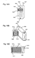
- Semiconductor devices of this type include a video camera, a still camera, a car navigation system, a personal computer, and a portable information terminal (such as a mobile computer and a cellular telephone), examples of which are shown in Figs. 16A to 16C and Figs. 17A to 17E .
- Fig. 16A shows a cellular telephone formed of a main body 1601, a voice output portion 1602, a voice input portion 1603, a reflection type liquid crystal panel 1604, an optical fiber array 1605, a control switch 1606, and an antenna 1607.
- Fig. 16B shows a video camera formed of a main body 1608, a reflection type liquid crystal panel 1609, an optical fiber array 1610, a voice input portion 1611, a control switch 1612, a battery 1613, and an image reception portion 1614.
- Fig. 16C shows a mobile computer formed of a main body 1615, a reflection type liquid crystal panel 1616, an optical fiber array 1617, a camera portion 1618, an image reception portion 1619, and a control switch 1620.
- Fig. 17A shows a personal computer formed of a main body 2001, an image input portion 2002, a reflection type liquid crystal panel 2003, a keyboard 2004, and an optical fiber array 2005.
- Fig. 17B shows a goggles type display formed of a main body 2101, a reflection type liquid crystal panel 2102, an arm portion 2103, and an optical fiber array 2104.
- Fig. 17C shows a player using a recording medium with a program recorded therein (hereinafter referred to as a recording medium) and formed of a main body 2201, a reflection type liquid crystal panel 2202, a speaker portion 2203, a recording medium 2204, a control switch 2205, and an optical fiber array 2206.
- a recording medium with a program recorded therein (hereinafter referred to as a recording medium) and formed of a main body 2201, a reflection type liquid crystal panel 2202, a speaker portion 2203, a recording medium 2204, a control switch 2205, and an optical fiber array 2206.
- a DVD digital versatile disc
- CD compact disc
- Fig. 17D shows a digital camera formed of a main body 2301, a reflection type liquid crystal panel 2302, a viewfinder 2303, a control switch 2304, an optical fiber array 2305, and an image reception portion (not shown).
- Fig. 17E shows a portable electronic book formed of a main body 2401, a reflection type liquid crystal panels 2402 and 2403, a recording medium 2404, a control switch 2405, an antenna 2406, and an optical fiber array 2407.
- a reflection type semiconductor display device of the present invention light other than incident light on a liquid crystal panel can be taken in to be an auxiliary light source using optical fibers, and thus, display of high quality level can be made even indoors or in a place where light is faint.
Landscapes
- Physics & Mathematics (AREA)
- General Physics & Mathematics (AREA)
- Optics & Photonics (AREA)
- Nonlinear Science (AREA)
- Mathematical Physics (AREA)
- Chemical & Material Sciences (AREA)
- Crystallography & Structural Chemistry (AREA)
- Liquid Crystal (AREA)
- Devices For Indicating Variable Information By Combining Individual Elements (AREA)
Claims (14)
- Reflektierende Anzeigevorrichtung, die umfasst:ein erstes Substrat (301, 401);eine Vielzahl von reflektierenden Pixelelektroden (305, 405) über dem ersten Substrate (301, 401);eine Lichtführungsplatte (307, 408) über der Vielzahl von reflektierenden Pixelelektroden (305, 405);einen Flüssigkristall (306, 406), der zwischen dem ersten Substrat (301, 401) und der Lichtführungsplatte (307, 408) angeordnet ist;ein Glasfaserkabel (801), das eine Vielzahl von Glasfasern (802) umfasst, wobei das Glasfaserkabel (801) ein erstes Ende und ein zweites Ende aufweist; undein Mikrolinsenarray (803), das sich an dem zweiten Ende befindet, wobei das erste Ende im Betrieb an einem Rand der Lichtführungsplatte (307, 408) angeschlossen ist und das zweite Ende so angeordnet ist, dass Außenlicht durch das zweite Ende einfallen kann.
- Reflektierende Anzeigevorrichtung nach Anspruch 1, die ferner ein zweites Substrat (407), das zwischen dem Flüssigkristall (406) und der Lichtführungsplatte (408) angeordnet ist, umfasst.
- Reflektierende Anzeigevorrichtung nach Anspruch 1 oder 2, wobei die reflektierenden Pixelelektroden (305, 405) an Dünnschichttransistoren (304, 404) angeschlossen sind.
- Reflektierende Anzeigevorrichtung nach Anspruch 2, die ferner eine durchsichtige leitende Schicht unter dem zweiten Substrat umfasst.
- Reflektierende Anzeigevorrichtung nach Anspruch 1 oder 2, die ferner ein Frontlicht (1409) umfasst.
- Reflektierende Anzeigevorrichtung nach Anspruch 5, wobei das Frontlicht eine LED umfasst.
- Mobiltelefon, das die reflektierende Anzeigevorrichtung nach Anspruch 1 oder 2 aufweist.
- Videokamera, die die reflektierende Anzeigevorrichtung nach Anspruch 1 oder 2 aufweist.
- Mobilcomputer, der die reflektierende Anzeigevorrichtung nach Anspruch 1 oder 2 aufweist.
- Personalcomputer, der die reflektierende Anzeigevorrichtung nach Anspruch 1 oder 2 aufweist.
- Brillendisplay, das die reflektierende Anzeigevorrichtung nach Anspruch 1 oder 2 aufweist.
- Spieler, der ein Aufnahmemedium, das die reflektierende Anzeigevorrichtung nach Anspruch 1 oder 2 aufweist, verwendet.
- Digitalkamera, die die reflektierende Anzeigevorrichtung nach Anspruch 1 oder 2 aufweist.
- Tragbares elektronisches Buch, das die reflektierende Anzeigevorrichtung nach Anspruch 1 oder 2 aufweist.
Applications Claiming Priority (2)
| Application Number | Priority Date | Filing Date | Title |
|---|---|---|---|
| JP28230298 | 1998-10-05 | ||
| JP28230298 | 1998-10-05 |
Publications (3)
| Publication Number | Publication Date |
|---|---|
| EP0992837A2 EP0992837A2 (de) | 2000-04-12 |
| EP0992837A3 EP0992837A3 (de) | 2000-06-28 |
| EP0992837B1 true EP0992837B1 (de) | 2010-06-16 |
Family
ID=17650661
Family Applications (1)
| Application Number | Title | Priority Date | Filing Date |
|---|---|---|---|
| EP99118795A Expired - Lifetime EP0992837B1 (de) | 1998-10-05 | 1999-09-23 | Reflektierende Halbleitervorrichtung |
Country Status (3)
| Country | Link |
|---|---|
| US (4) | US6407785B1 (de) |
| EP (1) | EP0992837B1 (de) |
| DE (1) | DE69942499D1 (de) |
Families Citing this family (107)
| Publication number | Priority date | Publication date | Assignee | Title |
|---|---|---|---|---|
| DE69942499D1 (de) * | 1998-10-05 | 2010-07-29 | Semiconductor Energy Lab | Reflektierende Halbleitervorrichtung |
| DE10000300A1 (de) * | 1999-06-11 | 2000-12-14 | Mannesmann Vdo Ag | Flüssigkristallanzeige |
| US7697052B1 (en) | 1999-02-17 | 2010-04-13 | Semiconductor Energy Laboratory Co., Ltd. | Electronic view finder utilizing an organic electroluminescence display |
| EP1063561A1 (de) | 1999-06-11 | 2000-12-27 | Mannesmann VDO Aktiengesellschaft | Flüssigkristallanzeige |
| US20050007515A1 (en) * | 2000-06-26 | 2005-01-13 | Faris Sadeg M. | Backlight for a liquid crystal display having high light-recycling efficiency |
| KR100706752B1 (ko) * | 2000-08-09 | 2007-04-11 | 삼성전자주식회사 | 반사형 액정표시장치 |
| GB2372868B (en) * | 2001-03-02 | 2004-10-06 | Hewlett Packard Co | A display |
| US6988806B2 (en) * | 2001-06-08 | 2006-01-24 | Infocus Corporation | Instant-on projector |
| US7567384B2 (en) * | 2001-06-08 | 2009-07-28 | Infocus Corporation | Method and apparatus for combining light paths of like-colored light sources |
| US6688747B2 (en) * | 2001-06-08 | 2004-02-10 | Infocus Corporation | Achieving color balance in image projection systems by injecting compensating light |
| CN1643439A (zh) * | 2002-03-14 | 2005-07-20 | 日本电气株式会社 | 光调制显示器件、其制作方法以及装有此光调制显示器件的显示装置 |
| JP3946062B2 (ja) * | 2002-03-18 | 2007-07-18 | シャープ株式会社 | 表示装置およびその製造方法 |
| FR2843792B1 (fr) * | 2002-08-20 | 2005-04-08 | Thales Sa | Boite a lumiere a haute luminance pour visualisations |
| WO2004051609A2 (en) * | 2002-11-29 | 2004-06-17 | Magink Display Technologies Ltd. | Display panel and large display using such display panel |
| TWI289708B (en) | 2002-12-25 | 2007-11-11 | Qualcomm Mems Technologies Inc | Optical interference type color display |
| US20040204151A1 (en) * | 2002-12-30 | 2004-10-14 | Sivakumar Muthuswamy | Method and apparatus for advising a user of a wireless device as to a connection status thereof |
| US6919635B2 (en) * | 2003-11-04 | 2005-07-19 | International Business Machines Corporation | High density microvia substrate with high wireability |
| ATE552521T1 (de) | 2003-12-19 | 2012-04-15 | Barco Nv | Breitbandige reflektive anzeigevorrichtung |
| US7342705B2 (en) | 2004-02-03 | 2008-03-11 | Idc, Llc | Spatial light modulator with integrated optical compensation structure |
| GB0403367D0 (en) * | 2004-02-16 | 2004-03-17 | Microsharp Corp Ltd | Light-coupling device for a display backlight assembly |
| US7706050B2 (en) | 2004-03-05 | 2010-04-27 | Qualcomm Mems Technologies, Inc. | Integrated modulator illumination |
| US20050259216A1 (en) * | 2004-05-20 | 2005-11-24 | Alps Electric (North America), Inc. | Optical switching device using holographic polymer dispersed liquid crystals |
| US7301601B2 (en) * | 2004-05-20 | 2007-11-27 | Alps Electric (Usa) Inc. | Optical switching device using holographic polymer dispersed liquid crystals |
| US7355780B2 (en) | 2004-09-27 | 2008-04-08 | Idc, Llc | System and method of illuminating interferometric modulators using backlighting |
| US7750886B2 (en) * | 2004-09-27 | 2010-07-06 | Qualcomm Mems Technologies, Inc. | Methods and devices for lighting displays |
| US7813026B2 (en) * | 2004-09-27 | 2010-10-12 | Qualcomm Mems Technologies, Inc. | System and method of reducing color shift in a display |
| US7561323B2 (en) * | 2004-09-27 | 2009-07-14 | Idc, Llc | Optical films for directing light towards active areas of displays |
| US7643105B2 (en) * | 2005-03-25 | 2010-01-05 | Tai-Her Yang | Display system on reflective interaction guided by a light source |
| WO2006107989A2 (en) * | 2005-04-05 | 2006-10-12 | Advanced Lighting Technologies, Inc. | Fiber illumination system for back lighting |
| US7486854B2 (en) | 2006-01-24 | 2009-02-03 | Uni-Pixel Displays, Inc. | Optical microstructures for light extraction and control |
| US7603001B2 (en) | 2006-02-17 | 2009-10-13 | Qualcomm Mems Technologies, Inc. | Method and apparatus for providing back-lighting in an interferometric modulator display device |
| US20080006833A1 (en) * | 2006-06-02 | 2008-01-10 | Semiconductor Energy Laboratory Co., Ltd. | Lighting device and liquid crystal display device |
| US7766498B2 (en) | 2006-06-21 | 2010-08-03 | Qualcomm Mems Technologies, Inc. | Linear solid state illuminator |
| US7845841B2 (en) * | 2006-08-28 | 2010-12-07 | Qualcomm Mems Technologies, Inc. | Angle sweeping holographic illuminator |
| WO2008045200A2 (en) | 2006-10-06 | 2008-04-17 | Qualcomm Mems Technologies, Inc. | Optical loss structure integrated in an illumination apparatus of a display |
| US7855827B2 (en) | 2006-10-06 | 2010-12-21 | Qualcomm Mems Technologies, Inc. | Internal optical isolation structure for integrated front or back lighting |
| EP2069838A2 (de) | 2006-10-06 | 2009-06-17 | Qualcomm Mems Technologies, Inc. | Beleuchtungsvorrichtung mit eingebautem lichtkoppler |
| KR20090094241A (ko) * | 2006-10-06 | 2009-09-04 | 퀄컴 엠이엠스 테크놀로지스, 인크. | 박형 라이트 바 및 그 제조방법 |
| US8107155B2 (en) | 2006-10-06 | 2012-01-31 | Qualcomm Mems Technologies, Inc. | System and method for reducing visual artifacts in displays |
| WO2008045207A2 (en) * | 2006-10-06 | 2008-04-17 | Qualcomm Mems Technologies, Inc. | Light guide |
| US7864395B2 (en) | 2006-10-27 | 2011-01-04 | Qualcomm Mems Technologies, Inc. | Light guide including optical scattering elements and a method of manufacture |
| US7777954B2 (en) | 2007-01-30 | 2010-08-17 | Qualcomm Mems Technologies, Inc. | Systems and methods of providing a light guiding layer |
| US7733439B2 (en) * | 2007-04-30 | 2010-06-08 | Qualcomm Mems Technologies, Inc. | Dual film light guide for illuminating displays |
| US8184238B2 (en) * | 2007-09-04 | 2012-05-22 | Panasonic Corporation | Planar illumination device and liquid crystal display device using the same |
| US8941631B2 (en) | 2007-11-16 | 2015-01-27 | Qualcomm Mems Technologies, Inc. | Simultaneous light collection and illumination on an active display |
| US7949213B2 (en) | 2007-12-07 | 2011-05-24 | Qualcomm Mems Technologies, Inc. | Light illumination of displays with front light guide and coupling elements |
| US8068710B2 (en) | 2007-12-07 | 2011-11-29 | Qualcomm Mems Technologies, Inc. | Decoupled holographic film and diffuser |
| US8654061B2 (en) | 2008-02-12 | 2014-02-18 | Qualcomm Mems Technologies, Inc. | Integrated front light solution |
| WO2009102731A2 (en) | 2008-02-12 | 2009-08-20 | Qualcomm Mems Technologies, Inc. | Devices and methods for enhancing brightness of displays using angle conversion layers |
| JP2011517118A (ja) * | 2008-04-11 | 2011-05-26 | クォルコム・メムズ・テクノロジーズ・インコーポレーテッド | Pvの美観および効率を改善する方法 |
| WO2009129264A1 (en) | 2008-04-15 | 2009-10-22 | Qualcomm Mems Technologies, Inc. | Light with bi-directional propagation |
| US8118468B2 (en) * | 2008-05-16 | 2012-02-21 | Qualcomm Mems Technologies, Inc. | Illumination apparatus and methods |
| RU2010147803A (ru) * | 2008-05-28 | 2012-07-10 | Квалкомм Мемс Текнолоджис, Инк. (Us) | Подсвечивающие устройства для фронтальной подсветки и способы их изготовления |
| CN102047035A (zh) * | 2008-06-04 | 2011-05-04 | 高通Mems科技公司 | 用于棱镜前光的减少边缘阴影的方法 |
| US20100051089A1 (en) * | 2008-09-02 | 2010-03-04 | Qualcomm Mems Technologies, Inc. | Light collection device with prismatic light turning features |
| US8358266B2 (en) | 2008-09-02 | 2013-01-22 | Qualcomm Mems Technologies, Inc. | Light turning device with prismatic light turning features |
| US20100066941A1 (en) * | 2008-09-16 | 2010-03-18 | Illumitex, Inc. | Hybrid lighting panel and lcd system |
| JP5342016B2 (ja) | 2009-01-13 | 2013-11-13 | クォルコム・メムズ・テクノロジーズ・インコーポレーテッド | 大面積光パネル及びスクリーン |
| US8905610B2 (en) | 2009-01-26 | 2014-12-09 | Flex Lighting Ii, Llc | Light emitting device comprising a lightguide film |
| US8172417B2 (en) | 2009-03-06 | 2012-05-08 | Qualcomm Mems Technologies, Inc. | Shaped frontlight reflector for use with display |
| CN102449513B (zh) | 2009-05-29 | 2015-01-21 | 高通Mems科技公司 | 照明装置及其制造方法 |
| TW201113476A (en) * | 2009-07-29 | 2011-04-16 | Illumitex Inc | Orthogonally separable light bar |
| US20110169428A1 (en) * | 2010-01-08 | 2011-07-14 | Qualcomm Mems Technologies, Inc. | Edge bar designs to mitigate edge shadow artifact |
| US9651729B2 (en) | 2010-04-16 | 2017-05-16 | Flex Lighting Ii, Llc | Reflective display comprising a frontlight with extraction features and a light redirecting optical element |
| US9097832B2 (en) * | 2010-04-27 | 2015-08-04 | Xiao Lin Yu | Liquid crystal display (LCD) system and method |
| US8402647B2 (en) | 2010-08-25 | 2013-03-26 | Qualcomm Mems Technologies Inc. | Methods of manufacturing illumination systems |
| WO2012068543A1 (en) * | 2010-11-18 | 2012-05-24 | Flex Lighting Ii, Llc | Light emitting device comprising a lightguide film and aligned coupling lightguides |
| US8902484B2 (en) | 2010-12-15 | 2014-12-02 | Qualcomm Mems Technologies, Inc. | Holographic brightness enhancement film |
| CA2829388C (en) | 2011-03-09 | 2018-09-25 | Flex Lighting Ii, Llc | Light emitting device with adjustable light output profile |
| TW201319677A (zh) * | 2011-11-02 | 2013-05-16 | Hon Hai Prec Ind Co Ltd | 具有光補償模組的反射型顯示裝置 |
| US8860910B2 (en) * | 2012-11-02 | 2014-10-14 | Shenzhen China Star Optoelectronics Technology Co., Ltd. | Backlight module and display apparatus |
| JP5851979B2 (ja) * | 2012-12-26 | 2016-02-03 | 株式会社ジャパンディスプレイ | 表示装置 |
| US11009646B2 (en) | 2013-03-12 | 2021-05-18 | Azumo, Inc. | Film-based lightguide with interior light directing edges in a light mixing region |
| US10247870B2 (en) | 2015-05-04 | 2019-04-02 | Himax Display, Inc. | Wearable display apparatus comprising an optical assembly having an optical integrator rod |
| US10860142B1 (en) | 2015-08-27 | 2020-12-08 | Apple Inc. | Light-based devices with light guide arrays |
| DE102015115265A1 (de) * | 2015-09-10 | 2017-03-16 | Schott Ag | Linienleuchte |
| WO2017064593A1 (en) | 2015-10-12 | 2017-04-20 | Semiconductor Energy Laboratory Co., Ltd. | Display device and manufacturing method thereof |
| WO2017081575A1 (en) | 2015-11-11 | 2017-05-18 | Semiconductor Energy Laboratory Co., Ltd. | Display device and method for manufacturing the same |
| CN106772762A (zh) * | 2016-12-27 | 2017-05-31 | 惠科股份有限公司 | 背光模块 |
| US10160379B2 (en) * | 2016-12-30 | 2018-12-25 | Valeo North America, Inc. | Integration of side reflex and light pipe side marker |
| US11309370B1 (en) | 2018-01-12 | 2022-04-19 | Apple Inc. | Electronic device displays with curved surfaces |
| US11003015B1 (en) | 2018-03-05 | 2021-05-11 | Apple Inc. | Electronic device with a light guiding layer |
| US11737307B1 (en) | 2018-06-05 | 2023-08-22 | Apple Inc. | Electronic devices having curved displays with supporting frames |
| US11054861B2 (en) | 2018-06-11 | 2021-07-06 | Apple Inc. | Electronic devices having displays with expanded edges |
| US11963425B1 (en) | 2018-07-10 | 2024-04-16 | Apple Inc. | Electronic devices having displays with curved surfaces |
| US11353652B1 (en) | 2018-07-10 | 2022-06-07 | Apple Inc. | Electronic devices having displays with curved surfaces and image transport layers |
| US11388329B1 (en) | 2018-07-17 | 2022-07-12 | Apple Inc. | Electronic devices having displays with image transport layers |
| US10937987B1 (en) | 2018-07-20 | 2021-03-02 | Apple Inc. | Electronic devices having displays with tilted anodes |
| US11619779B1 (en) | 2018-08-10 | 2023-04-04 | Apple Inc. | Methods for forming image transport layers |
| CN113272693B (zh) | 2018-08-30 | 2023-06-13 | 阿祖莫公司 | 具有角度变化的漫射膜的基于膜的前光源 |
| US11810534B1 (en) | 2018-09-14 | 2023-11-07 | Apple Inc. | Distortion control in displays with optical coupling layers |
| US11436964B1 (en) | 2018-11-13 | 2022-09-06 | Apple Inc. | Electronic devices having image transport layers and electrical components |
| US11817025B1 (en) | 2018-11-13 | 2023-11-14 | Apple Inc. | Electronic devices having housings with image transport layers |
| US12101426B1 (en) | 2018-11-13 | 2024-09-24 | Apple Inc. | Electronic devices having vertical image transport layers |
| US11516908B1 (en) | 2018-11-13 | 2022-11-29 | Apple Inc. | Electronic devices having image transport layers with embedded circuitry |
| WO2020123539A1 (en) | 2018-12-11 | 2020-06-18 | Flex Lighting Ii, Llc | Front illumination lightguide with a diffusely reflective release liner |
| CN113678035B (zh) | 2019-01-03 | 2024-10-18 | 阿祖莫公司 | 包括产生多个照明峰值的光导和光转向膜的反射型显示器 |
| CN117891020A (zh) | 2019-01-09 | 2024-04-16 | 阿祖莫公司 | 包括以不同的折叠角折叠的耦合光导的反射型显示器 |
| US11844236B2 (en) | 2019-07-12 | 2023-12-12 | Semiconductor Energy Laboratory Co., Ltd. | Functional panel, display device, input/output device, and data processing device |
| US11513274B2 (en) | 2019-08-01 | 2022-11-29 | Azumo, Inc. | Lightguide with a light input edge between lateral edges of a folded strip |
| US11247421B1 (en) | 2019-08-20 | 2022-02-15 | Apple Inc. | Single-step extrusion of fiber optic plates for electronic devices |
| US11513554B1 (en) | 2019-08-23 | 2022-11-29 | Apple Inc. | Electronic devices having displays with borders of image transport material |
| US11774644B1 (en) | 2019-08-29 | 2023-10-03 | Apple Inc. | Electronic devices with image transport layers having light absorbing material |
| US11997766B2 (en) | 2019-10-11 | 2024-05-28 | Semiconductor Energy Laboratory Co., Ltd. | Functional panel, display device, input/output device, and data processing device |
| US11525955B1 (en) | 2020-06-05 | 2022-12-13 | Apple Inc. | Electronic devices with drawn sheet-packed coherent fiber bundles |
| US12571956B2 (en) | 2020-09-29 | 2026-03-10 | Azumo, Inc. | Manufacturing a lightguide with cut lateral edges |
| CN113885249B (zh) * | 2021-11-04 | 2022-07-12 | 厦门天马微电子有限公司 | 显示模组和显示装置 |
Family Cites Families (28)
| Publication number | Priority date | Publication date | Assignee | Title |
|---|---|---|---|---|
| US4212048A (en) * | 1978-06-16 | 1980-07-08 | General Electric Company | Illuminator for reflective dichroic liquid crystal displays |
| DE3102626A1 (de) | 1981-01-27 | 1982-08-19 | Siemens AG, 1000 Berlin und 8000 München | "passive elektrooptische anzeigevorrichtung" |
| DE3314323A1 (de) | 1983-04-20 | 1984-10-31 | Robert Bosch Gmbh, 7000 Stuttgart | Vorrichtung zur ausleuchtung passiver anzeigen |
| JPS609330A (ja) | 1983-06-27 | 1985-01-18 | 株式会社東芝 | 系統切換制御装置 |
| US4911536A (en) * | 1986-05-08 | 1990-03-27 | Ditzik Richard J | Interactive graphic comunications terminal |
| US5121232A (en) * | 1989-10-18 | 1992-06-09 | Asahi Kogaku Kogyo Kabushiki Kaisha | Displaying device having two separate light receiving portions for receiving the external light and the light emitted by a light source |
| US5181130A (en) * | 1990-01-09 | 1993-01-19 | Hewlett-Packard Company | Fiber optic faceplate liquid crystal display |
| JPH03248125A (ja) * | 1990-02-26 | 1991-11-06 | Sharp Corp | 液晶表示素子 |
| US5101325A (en) * | 1990-03-20 | 1992-03-31 | General Electric Company | Uniform illumination of large, thin surfaces particularly suited for automotive applications |
| JPH0429291A (ja) * | 1990-05-25 | 1992-01-31 | Sumitomo Electric Ind Ltd | 導光板 |
| GB2246231A (en) | 1990-07-20 | 1992-01-22 | Marconi Gec Ltd | Liquid crystal displays. |
| JP2812851B2 (ja) | 1993-03-24 | 1998-10-22 | シャープ株式会社 | 反射型液晶表示装置 |
| US5329386A (en) * | 1993-04-13 | 1994-07-12 | Hewlett-Packard Company | Fiber-optic faceplate with tilted fibers |
| CA2121653C (en) * | 1993-05-05 | 1997-05-13 | Kevin D. Kaschke | Optical fiber light emitting apparatus |
| JPH0772446A (ja) * | 1993-09-01 | 1995-03-17 | Sharp Corp | 表示システム |
| US5982540A (en) * | 1994-03-16 | 1999-11-09 | Enplas Corporation | Surface light source device with polarization function |
| JPH07301714A (ja) * | 1994-05-09 | 1995-11-14 | Beam Soken:Kk | 面放光装置 |
| JPH08179300A (ja) * | 1994-12-22 | 1996-07-12 | Sony Corp | カラー表示装置 |
| US5765934A (en) * | 1995-08-04 | 1998-06-16 | Mitsubishi Denki Kabushiki Kaisha | Projection type display |
| US5706066A (en) * | 1995-10-16 | 1998-01-06 | Sharp Kabushiki Kaisha | Deflecting device and projection-type display unit using same |
| US5703664A (en) * | 1995-10-23 | 1997-12-30 | Motorola, Inc. | Integrated electro-optic package for reflective spatial light modulators |
| US5760852A (en) * | 1995-11-03 | 1998-06-02 | Hughes Electronics Corporation | Laser-hardened eye protection goggles |
| TW446843B (en) * | 1996-01-10 | 2001-07-21 | Sumitomo Chemical Co | A microlens-array, production method thereof, and liquid crystal display device using the same |
| JPH09325221A (ja) * | 1996-04-04 | 1997-12-16 | Hitachi Cable Ltd | 照明装置 |
| US5930044A (en) * | 1997-01-09 | 1999-07-27 | U.S. Philips Corporation | Deflecting element having a switchable liquid crystalline material |
| US6151089A (en) * | 1998-01-20 | 2000-11-21 | Sony Corporation | Reflection type display with light waveguide with inclined and planar surface sections |
| DE69942499D1 (de) * | 1998-10-05 | 2010-07-29 | Semiconductor Energy Lab | Reflektierende Halbleitervorrichtung |
| JP2000280527A (ja) * | 1999-04-02 | 2000-10-10 | Mitsubishi Electric Corp | 光プリントヘッド |
-
1999
- 1999-09-23 DE DE69942499T patent/DE69942499D1/de not_active Expired - Lifetime
- 1999-09-23 EP EP99118795A patent/EP0992837B1/de not_active Expired - Lifetime
- 1999-09-29 US US09/407,796 patent/US6407785B1/en not_active Expired - Lifetime
-
2002
- 2002-04-23 US US10/127,854 patent/US6784952B2/en not_active Expired - Fee Related
-
2004
- 2004-07-20 US US10/895,009 patent/US6999137B2/en not_active Expired - Fee Related
-
2005
- 2005-12-12 US US11/301,127 patent/US7253854B2/en not_active Expired - Fee Related
Also Published As
| Publication number | Publication date |
|---|---|
| US20060092354A1 (en) | 2006-05-04 |
| US20020176035A1 (en) | 2002-11-28 |
| EP0992837A2 (de) | 2000-04-12 |
| US20040257503A1 (en) | 2004-12-23 |
| EP0992837A3 (de) | 2000-06-28 |
| US6407785B1 (en) | 2002-06-18 |
| US6784952B2 (en) | 2004-08-31 |
| US6999137B2 (en) | 2006-02-14 |
| DE69942499D1 (de) | 2010-07-29 |
| US7253854B2 (en) | 2007-08-07 |
Similar Documents
| Publication | Publication Date | Title |
|---|---|---|
| EP0992837B1 (de) | Reflektierende Halbleitervorrichtung | |
| JP2000181367A (ja) | 反射型半導体表示装置 | |
| CN100437273C (zh) | 前光源及电子设备 | |
| CN100378537C (zh) | 背光组件和具有该背光组件的液晶显示装置 | |
| US7517128B2 (en) | Backlight assembly removing dark areas and display device provided with the same | |
| US8446541B2 (en) | Portable computer | |
| CN101126494B (zh) | 照明装置、液晶装置及电子设备 | |
| WO2012071749A1 (zh) | 拼接式导光板构造及背光模块 | |
| US20150362652A1 (en) | Lighting device, display device, and television receiving device | |
| KR20080107633A (ko) | 액정 표시 장치 | |
| JP2006350301A (ja) | 液晶表示装置 | |
| JP2005249942A (ja) | 表示装置 | |
| KR20120068499A (ko) | 백라이트 유닛 및 이를 구비한 액정표시장치 | |
| CN110471203B (zh) | 显示装置及电子设备 | |
| JP2009158274A (ja) | Led光源装置、及びこのled光源装置を備える液晶表示装置 | |
| TWI403802B (zh) | 具有改良光導板之背光組件及具有該背光組件之顯示器裝置 | |
| US11309370B1 (en) | Electronic device displays with curved surfaces | |
| US20150022759A1 (en) | Display with Radioluminescent Backlight Unit | |
| US20190196089A1 (en) | Display apparatus with backlight unit and method of fabricating backlight unit | |
| JP2009043574A (ja) | 光学デバイス及び液晶表示装置 | |
| JPH0854517A (ja) | 導光板及びこれを用いた液晶表示装置 | |
| JP2007047811A (ja) | 表示装置 | |
| KR20120075115A (ko) | 도광판, 이를 구비한 백라이트 유닛 및 이들을 포함하는 액정표시장치 | |
| KR20080039637A (ko) | 발광 다이오드 유닛, 이를 이용한 백라이트 유닛 및 이를구비하는 표시 장치 | |
| KR20150039034A (ko) | 액정표시장치 및 그 제조방법 |
Legal Events
| Date | Code | Title | Description |
|---|---|---|---|
| PUAI | Public reference made under article 153(3) epc to a published international application that has entered the european phase |
Free format text: ORIGINAL CODE: 0009012 |
|
| AK | Designated contracting states |
Kind code of ref document: A2 Designated state(s): DE FR GB NL |
|
| AX | Request for extension of the european patent |
Free format text: AL;LT;LV;MK;RO;SI |
|
| PUAL | Search report despatched |
Free format text: ORIGINAL CODE: 0009013 |
|
| AK | Designated contracting states |
Kind code of ref document: A3 Designated state(s): AT BE CH CY DE DK ES FI FR GB GR IE IT LI LU MC NL PT SE |
|
| AX | Request for extension of the european patent |
Free format text: AL;LT;LV;MK;RO;SI |
|
| 17P | Request for examination filed |
Effective date: 20001208 |
|
| AKX | Designation fees paid |
Free format text: DE FR GB NL |
|
| GRAP | Despatch of communication of intention to grant a patent |
Free format text: ORIGINAL CODE: EPIDOSNIGR1 |
|
| GRAS | Grant fee paid |
Free format text: ORIGINAL CODE: EPIDOSNIGR3 |
|
| GRAA | (expected) grant |
Free format text: ORIGINAL CODE: 0009210 |
|
| AK | Designated contracting states |
Kind code of ref document: B1 Designated state(s): DE FR GB NL |
|
| REF | Corresponds to: |
Ref document number: 69942499 Country of ref document: DE Date of ref document: 20100729 Kind code of ref document: P |
|
| REG | Reference to a national code |
Ref country code: NL Ref legal event code: VDEP Effective date: 20100616 |
|
| PG25 | Lapsed in a contracting state [announced via postgrant information from national office to epo] |
Ref country code: NL Free format text: LAPSE BECAUSE OF FAILURE TO SUBMIT A TRANSLATION OF THE DESCRIPTION OR TO PAY THE FEE WITHIN THE PRESCRIBED TIME-LIMIT Effective date: 20100616 |
|
| PLBE | No opposition filed within time limit |
Free format text: ORIGINAL CODE: 0009261 |
|
| STAA | Information on the status of an ep patent application or granted ep patent |
Free format text: STATUS: NO OPPOSITION FILED WITHIN TIME LIMIT |
|
| 26N | No opposition filed |
Effective date: 20110317 |
|
| REG | Reference to a national code |
Ref country code: DE Ref legal event code: R097 Ref document number: 69942499 Country of ref document: DE Effective date: 20110316 |
|
| PGFP | Annual fee paid to national office [announced via postgrant information from national office to epo] |
Ref country code: GB Payment date: 20120919 Year of fee payment: 14 |
|
| PGFP | Annual fee paid to national office [announced via postgrant information from national office to epo] |
Ref country code: FR Payment date: 20120926 Year of fee payment: 14 |
|
| GBPC | Gb: european patent ceased through non-payment of renewal fee |
Effective date: 20130923 |
|
| REG | Reference to a national code |
Ref country code: FR Ref legal event code: ST Effective date: 20140530 |
|
| PG25 | Lapsed in a contracting state [announced via postgrant information from national office to epo] |
Ref country code: GB Free format text: LAPSE BECAUSE OF NON-PAYMENT OF DUE FEES Effective date: 20130923 |
|
| PG25 | Lapsed in a contracting state [announced via postgrant information from national office to epo] |
Ref country code: FR Free format text: LAPSE BECAUSE OF NON-PAYMENT OF DUE FEES Effective date: 20130930 |
|
| PGFP | Annual fee paid to national office [announced via postgrant information from national office to epo] |
Ref country code: DE Payment date: 20150916 Year of fee payment: 17 |
|
| REG | Reference to a national code |
Ref country code: DE Ref legal event code: R119 Ref document number: 69942499 Country of ref document: DE |
|
| PG25 | Lapsed in a contracting state [announced via postgrant information from national office to epo] |
Ref country code: DE Free format text: LAPSE BECAUSE OF NON-PAYMENT OF DUE FEES Effective date: 20170401 |