EP0993016A2 - Plasma-Anzeige-Vorrichtung und Verfahren zu deren Zerlegung - Google Patents
Plasma-Anzeige-Vorrichtung und Verfahren zu deren Zerlegung Download PDFInfo
- Publication number
- EP0993016A2 EP0993016A2 EP99118967A EP99118967A EP0993016A2 EP 0993016 A2 EP0993016 A2 EP 0993016A2 EP 99118967 A EP99118967 A EP 99118967A EP 99118967 A EP99118967 A EP 99118967A EP 0993016 A2 EP0993016 A2 EP 0993016A2
- Authority
- EP
- European Patent Office
- Prior art keywords
- panel
- pdp
- plasma display
- panels
- display panel
- Prior art date
- Legal status (The legal status is an assumption and is not a legal conclusion. Google has not performed a legal analysis and makes no representation as to the accuracy of the status listed.)
- Granted
Links
Images


Classifications
-
- H—ELECTRICITY
- H01—ELECTRIC ELEMENTS
- H01J—ELECTRIC DISCHARGE TUBES OR DISCHARGE LAMPS
- H01J11/00—Gas-filled discharge tubes with alternating current induction of the discharge, e.g. alternating current plasma display panels [AC-PDP]; Gas-filled discharge tubes without any main electrode inside the vessel; Gas-filled discharge tubes with at least one main electrode outside the vessel
- H01J11/20—Constructional details
- H01J11/48—Sealing, e.g. seals specially adapted for leading-in conductors
-
- G—PHYSICS
- G09—EDUCATION; CRYPTOGRAPHY; DISPLAY; ADVERTISING; SEALS
- G09F—DISPLAYING; ADVERTISING; SIGNS; LABELS OR NAME-PLATES; SEALS
- G09F9/00—Indicating arrangements for variable information in which the information is built-up on a support by selection or combination of individual elements
- G09F9/30—Indicating arrangements for variable information in which the information is built-up on a support by selection or combination of individual elements in which the desired character or characters are formed by combining individual elements
- G09F9/313—Indicating arrangements for variable information in which the information is built-up on a support by selection or combination of individual elements in which the desired character or characters are formed by combining individual elements being gas discharge devices
-
- H—ELECTRICITY
- H01—ELECTRIC ELEMENTS
- H01J—ELECTRIC DISCHARGE TUBES OR DISCHARGE LAMPS
- H01J11/00—Gas-filled discharge tubes with alternating current induction of the discharge, e.g. alternating current plasma display panels [AC-PDP]; Gas-filled discharge tubes without any main electrode inside the vessel; Gas-filled discharge tubes with at least one main electrode outside the vessel
- H01J11/10—AC-PDPs with at least one main electrode being out of contact with the plasma
- H01J11/12—AC-PDPs with at least one main electrode being out of contact with the plasma with main electrodes provided on both sides of the discharge space
-
- H—ELECTRICITY
- H01—ELECTRIC ELEMENTS
- H01J—ELECTRIC DISCHARGE TUBES OR DISCHARGE LAMPS
- H01J11/00—Gas-filled discharge tubes with alternating current induction of the discharge, e.g. alternating current plasma display panels [AC-PDP]; Gas-filled discharge tubes without any main electrode inside the vessel; Gas-filled discharge tubes with at least one main electrode outside the vessel
- H01J11/20—Constructional details
- H01J11/34—Vessels, containers or parts thereof, e.g. substrates
-
- H—ELECTRICITY
- H01—ELECTRIC ELEMENTS
- H01J—ELECTRIC DISCHARGE TUBES OR DISCHARGE LAMPS
- H01J9/00—Apparatus or processes specially adapted for the manufacture, installation, removal, maintenance of electric discharge tubes, discharge lamps, or parts thereof; Recovery of material from discharge tubes or lamps
- H01J9/50—Repairing or regenerating used or defective discharge tubes or lamps
-
- H—ELECTRICITY
- H01—ELECTRIC ELEMENTS
- H01J—ELECTRIC DISCHARGE TUBES OR DISCHARGE LAMPS
- H01J9/00—Apparatus or processes specially adapted for the manufacture, installation, removal, maintenance of electric discharge tubes, discharge lamps, or parts thereof; Recovery of material from discharge tubes or lamps
- H01J9/52—Recovery of material from discharge tubes or lamps
-
- Y—GENERAL TAGGING OF NEW TECHNOLOGICAL DEVELOPMENTS; GENERAL TAGGING OF CROSS-SECTIONAL TECHNOLOGIES SPANNING OVER SEVERAL SECTIONS OF THE IPC; TECHNICAL SUBJECTS COVERED BY FORMER USPC CROSS-REFERENCE ART COLLECTIONS [XRACs] AND DIGESTS
- Y02—TECHNOLOGIES OR APPLICATIONS FOR MITIGATION OR ADAPTATION AGAINST CLIMATE CHANGE
- Y02W—CLIMATE CHANGE MITIGATION TECHNOLOGIES RELATED TO WASTEWATER TREATMENT OR WASTE MANAGEMENT
- Y02W30/00—Technologies for solid waste management
- Y02W30/50—Reuse, recycling or recovery technologies
- Y02W30/60—Glass recycling
-
- Y—GENERAL TAGGING OF NEW TECHNOLOGICAL DEVELOPMENTS; GENERAL TAGGING OF CROSS-SECTIONAL TECHNOLOGIES SPANNING OVER SEVERAL SECTIONS OF THE IPC; TECHNICAL SUBJECTS COVERED BY FORMER USPC CROSS-REFERENCE ART COLLECTIONS [XRACs] AND DIGESTS
- Y02—TECHNOLOGIES OR APPLICATIONS FOR MITIGATION OR ADAPTATION AGAINST CLIMATE CHANGE
- Y02W—CLIMATE CHANGE MITIGATION TECHNOLOGIES RELATED TO WASTEWATER TREATMENT OR WASTE MANAGEMENT
- Y02W30/00—Technologies for solid waste management
- Y02W30/50—Reuse, recycling or recovery technologies
- Y02W30/82—Recycling of waste of electrical or electronic equipment [WEEE]
Definitions
- the present invention relates to recycling of a plasma display panel (hereinafter referred to as "PDP") employed in a computer terminal, a wall-hung television, and the like. More particularly, the invention relates to a method of disassembling a PDP, as well as a structure of PDP and a method of heating the PDP, with which the disassembling is made efficiently.
- PDP plasma display panel
- PDPs are self-luminous devices that are highly viewable, and have an advantage of making displays thin and large in screen size. For this reason, the PDPs gather a great expectation in these years as new display devices that replace the CRT's. Since surface-discharge type AC PDPs, in particular, are easy to manufacture, and have long operational life, many of them have been developed, manufactured, and marketed by numerous manufacturers.
- a PDP comprises a front panel 1 consisting of a glass substrate 3 provided on it with sustain electrodes 5, a dielectric layer 6 and a protection layer 7, and a back panel 2 also consisting of another glass substrate 4 provided on it with address electrodes 8, and barrier ribs 9. Further, phosphor 10 is provided within the ribs 9. Both panels are bonded together in their entire periphery with bonding material 13.
- An ordinary manufacturing process of the PDPs can be broken down into the steps of (a) producing front panels, (b) producing back panels, (c) assembling, sealing, vacuuming and gas charging.
- sustain electrodes 5 are formed on a glass substrate 3, and a dielectric layer 6 made of low temperature-melting glass containing lead oxide is formed on it by screen-printing and sintering.
- a back panel 2 is produced by forming address electrodes 8 on a glass substrate 4, and ribs 9 between the address electrodes 8 with low temperature-melting glass containing lead oxide. Phosphors 10 of red, green and blue colors are formed between the ribs 9.
- the front panel 1 and the back panel 2 are assembled together by placing one over another, and hermetically bonding them with bonding material 13 containing lead oxide.
- a PDP is completed finally by charging it with rare gas containing Xe, after a sufficient discharge of impure gases by vacuum-pumping an interior while heating the assembled PDP.
- the PDPs use a considerable amount of low temperature-melting glass containing lead oxide.
- Low temperature-melting glass is used for the dielectric layer in the front panel, the ribs in the back panel, and the bonding material for hermetically bonding the front panel and the back panel, to name a few examples.
- These PDPs are disposed of, if any flaw is found in them during the manufacturing process, or when they have reached their usable life in their end use application. However, they can not be discarded just as they are, but they shall be treated properly by establishments specialized in industrial waste disposal, because they contain lead.
- the discarded PDPs propound a problem of degrading quality of glass, if mixed with raw glass material, since they contain lead oxide.
- the present invention utilizes a thermal action and a chemical action in a process of disassembling the above-described PDPs.
- a first method adopts a component, which does not contract thermally at a softening temperature of bonding material used for hermetically bonding a front panel and a back panel, and is positioned between the two panels at the front and back, and that the two panels are separated with the use of this component. Further, the above-cited component maintains a gap with either one of the front panel and the back panel under a room ambient temperature, but the component either remains unchanged dimensionally, or expands when heated, thereby the component facilitates disassembly of the PDP.
- the present invention provides a groove on at least one of surfaces of the front panel and the back panel, for communicating the bonding material to an exterior of the PDP.
- Softened bonding material can be drawn out or absorbed through the groove.
- Another feature of the invention is to uniformalize heating and cooling of the PDP with a laminated graphite sheet provided on either an upper surface or a side surface of the PDP during the heating.
- a second method of the present invention is to separate a PDP into two glass substrates by immersing the PDP in etching solution that selectively dissolves only lead glass, and melting the bonding material.
- a groove is formed in a space between a perimeter of an image display screen and a bonded portion, in order to prevent the etching solution from invading into the display area in a center of the PDP by a capillary phenomenon.
- the groove is formed in a direction parallel with a longitudinal direction of electrodes formed on the substrates.
- the front panel and the back panel separated through the foregoing process are refurbished in a way that a deteriorated portion or a defective portion regains an original function.
- the refurbished front panel and back panel can be reutilized to make a PDP by hermetically bonding them again.
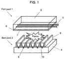
- Fig. 1 shows an exploded perspective view of a surface-discharge type AC PDP.
- the PDP comprises a front panel 1 and a back panel 2.
- the front panel 1 comprises sustain electrodes 5 for sustaining an electric discharge, a dielectric layer 6 provided over the sustain electrodes 5 and composed of low temperature-melting glass containing lead oxide, and a protection layer 7 composed of MgO, all formed on a glass substrate 3.
- the protection layer 7 of MgO has a function of protecting the dielectric layer 6 from sputtering due to electric discharge as well as a function of lowering a discharge voltage.
- the back panel 2 comprises address electrodes 8, ribs 9, and phosphors 10 of red, green and blue colors, all formed on another glass substrate 4.
- Material of the ribs 9 is low temperature-melting glass containing filler for maintaining its shape, and lead oxide. Both panels are held together and bonded in their entire periphery with bonding material 13, in an actual PDP, although Fig 1 illustrates the front panel 1 and the back panel 2 as being separated from each other in order to make them more comprehensible.
- the bonding material 13 also consists of low temperature-melting glass containing lead oxide.
- the PDP is completed when it is charged with rare gas such as Ne gas containing several percent of Xe, after having bonded hermetically with the bonding material 13, and expelled of gases by vacuum-pumping an interior while heating.
- a PDP has a portion where a front panel 1 and a back panel 2 do not overlap completely, as shown in Fig. 2. This portion is mainly used for leading terminals of address electrodes (not shown in the Fig. 2).
- the PDP can be illustrated as in a side view of Fig. 3, if it is held vertically and viewed from a direction of an arrow shown in Fig.2. There is a space 101 underneath the front panel 1, as viewed in this direction.
- the front panel 1 and the back panel 2 can be separated when a downward force is applied to the front panel 1 with a depressing part 102 provided on top of the front panel 1, as shown in Fig. 3, since bonding material 13 softens if the PDP is heated to 450°C or higher temperature, and more preferably at a temperature between 450°C and 550°C.
- the depressing part 102 is provided on the front panel 1 in the present exemplary embodiment, the same result can be attained by providing it on the back panel 2. Also, in the case that the front panel 1 and the back panel 2 overlap entirely, a provision of a spacer stand under one of the panels can produce a space under the other panel, thereby the same result can be attained.
- the depressing part 102 is used for applying a downward force, in the described exemplary embodiment, the same result can be attained by other means such as pulling up one of the panels.
- the PDP is placed vertically in the described embodiment, the same result can also be attained by placing the PDP horizontally, and either pushing or pulling one side of at least either one of the front panel 1 and the back panel 2 horizontally.
- Fig. 4 is a cross sectional view illustrating an essential portion of a PDP of the present exemplary embodiment.
- the PDP has a structure in which a front panel 1 and a back panel 2 are bonded together with bonding material 13.
- the bonding material 13 in this instance is composed of lead oxide and silicon oxide as primary components.
- the front panel 1 has a structure wherein sustain electrodes 5, a dielectric layer 6 and a protection layer 7 are provided on a glass substrate.
- the back panel 2 has a structure wherein address electrodes 8 and barrier walls 9 are provided on another panel. Also, phosphors 10 are provided within spaces provided between the ribs 9.
- the bonding material 13 bonds both panels in an entire perimeter of the PDP.
- the PDP is also provided with supporting components 22 between the front panel 1 and the back panel 2.
- the supporting components 22 in this exemplary embodiment are made of stainless steel, which generally has a thermal coefficient of expansion between 1 and 2 ⁇ 10 -5 / K.
- the PDP is placed in a high temperature ambient of 450°C or higher, and more preferably in a temperature range of 450°C and 550°C.
- the supporting components 22 expand thermally in this ambient, so as to widen a space between the front panel 1 and the back panel 2.
- the bonding material 13 softens in this high temperature ambient, and it dissociates from the panels, when it becomes unbearable to an expanding force of the supporting components 22. As a result, the PDP can be separated into the front panel 1 and the back panel 2 for reutilization.
- the supporting components 22 is provided at an outer side of the bonding material 13, as shown in Fig. 4, the same effect can be attained so long as it is provided at any position between the front panel 1 and the back panel 2.
- the present exemplary embodiment adopts the supporting components 22 made of stainless steel.
- the bonding material 13 not only softens, but also flags in this high temperature ambient, so as to shrink in height as shown in Fig. 5. Therefore, the same result can be achieved, even if the supporting components 22 are made of material having a small thermal coefficient of expansion, e.g. ceramic such as silicon nitride, and the like, instead of stainless steel.
- the present exemplary embodiment adopts a structure wherein the supporting components 22 are provided in advance between the front panel 1 and the back panel 2, they may be inserted between the front panel 1 and the back panel 2 immediately before heating the PDP for the purpose of separating the PDP in order to obtain the same effect.
- Fig. 6 is a cross sectional view showing an essential portion of a PDP of a third exemplary embodiment.
- each of supporting components 22 holds a gap 23 to a front panel 1, whereas it maintains a direct contact with a back panel 2.
- the supporting components 22 are made of stainless steel.
- the gaps 23 disappear due to a thermal expansion of the supporting components 22, when the PDP is heated to 450°C, which is a softening point of bonding material 13. Further continuation of the heating causes the supporting components 22 to produce a force of expansion, and the bonding material 13 dissociates from the panels when it becomes unbearable against this force.
- the supporting components 22 is capable of separating the two panels even if they produce only a small force of expansion, since the bonding material 13 shrinks in height as it flags, as shown in Fig. 5.
- Fig. 7 illustrates a side view of a PDP.
- a back panel 2 is provided with grooves 24 communicating bonding material 13 to an exterior of the PDP.
- the PDP is heated to a temperature of 450°C or higher, and more preferably at a temperature range of 450°C and 550°C.
- the PDP is then placed in an atmosphere of reduced pressure while maintaining the heated temperature. This draws out the bonding material 13 through the grooves 24, since the bonding material 13 has been softened at the heated temperature, and the exterior of the PDP is surrounded by the reduced pressure.
- the PDP can be separated into the front panel 1 and the back panel 2 for reutilization.
- the bonding material 13 is removed by reducing a surrounding pressure of the PDP, the same effect can be achieved with an aid of a nozzle-shaped tool for drawing the bonding material 13 by suction.
- the same effect can also be attained by inserting a metal mesh or a porous material such as alumina-ceramic into the grooves 24, so as to remove the bonding material 13 by absorption.
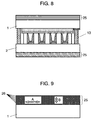
- Laminated graphite sheets 25 are placed on a front panel 1 and a back panel 2, as shown in Fig. 8.
- the laminated graphite sheets 25 used in this exemplary embodiment comprise a number of discrete graphite sheets 26 , which are stacked vertically in the same direction with the front panel 1 and the back panel 2, as shown in Fig. 9 (the back panel 2 is not shown in Fig. 9).
- the laminated graphite sheets 25 exhibit a relatively high thermal conductivity in a range of 10 to 87 W/m ⁇ K in an "A" direction, which is orthogonal to the direction of stacking, but a relatively low thermal conductivity in a range of 0.4 to 1.2 W/m ⁇ K in a "B" direction, which is the same direction as the stacking.
- the laminated graphite sheets 25 can prevent the panels and associated components from cracks or similar damages, which may occur otherwise when heating the PDP. Such cracks and damages can occur due to a lack of uniformity in temperature or a thermal shock in the substrates.
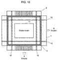
- a PDP of the present exemplary embodiment is provided with a groove 12 between a perimeter of an image display screen 11 and a bonded portion on at least either surface of a front panel 1 and a back panel 2, as shown in Fig. 10. This structure prevents etching solution from entering into the screen area by a capillary phenomenon.
- the image display screen 11 is located in a center area where the front panel 1 and the back panel 2 intersect, and bonding material 13 is applied in a boundary of intersection of the two panels.
- the groove 12 provided in the area between the bonded portion and the display screen, as shown in Fig. 10, can prevent the etching solution from advancing beyond the groove 12 to the screen side, even if the etching solution permeates through the bonding material 13, thereby protecting the display screen.
- a direction of the groove is in parallel with a longitudinal direction of electrodes on the front panel 1, on which at least the electrodes and a dielectric layer are formed.
- Providing the groove 12 in such direction can facilitate lead-out of the sustain electrodes to terminals, since the electrodes and the groove 12 do not cross with each other in a way of leading the electrodes to the terminals.
- a direction of the groove 12, when provided on the back panel 2 is in parallel with a longitudinal direction of electrodes on the back panel 2.
- Providing the groove in such direction also facilitate lead-out of the address electrodes to terminals, since the electrodes and the groove 12 do not cross with each other in a way of leading the electrodes to the terminals.
- the groove 12 in the present invention is more effective in preventing permeation of the solution by the capillary phenomenon, as the groove is made wider and deeper. If the groove is sized 1 mm in width and 0.5 mm in depth, for instance, it can not prevent permeation of the etching solution into the PDP, as the solution crosses over the groove.
- the groove can prevent permeation, if it is deepened to 1 mm while keeping the same width of 1 mm.
- an addition of surface-active agent into the etching solution can effectively reduce a rise of liquid level of the etching solution due to the capillary phenomenon.
- the groove can prevent permeation, if a surface-active agent is added into the etching solution, whereas the solution crosses over the groove if it does not contain surface-active agent.
- Fig. 13 illustrates a cross sectional view of the front panel 1.
- a pane of ordinary soda lime glass having a thickness of 2.8 mm is used for a glass panel 3, on which a groove 12 of 1 mm wide by 1.5 mm deep is cut at each side with a diamond cutter.
- the processing of grooves may be made by other method such as glass etching.
- the grooves are to be oriented in parallel with a longitudinal direction of sustain electrodes 5.
- the sustain electrodes 5 are then formed in a shape of stripes with Ag or Cr / Cu / Cr on the glass substrate 3, after processing the grooves as above.
- a dielectric layer 6 is formed next by printing low temperature-melting glass containing lead oxide over the sustain electrodes 5.
- FIG. 14 illustrates a cross sectional view of the back panel 2.
- a pane of soda glass having the same thickness of 2.8 mm is used for a glass substrate 4, on which a groove 14 of 1 mm wide by 1.5 mm deep is cut at each side with a diamond cutter.
- the grooves are also oriented in parallel with a longitudinal direction of address electrodes 8.
- the address electrodes 8 are then formed in a shape of stripes with Ag or Cr / Cu / Cr on the glass substrate 4, after processing the grooves as above.
- Ribs 9 are formed thereafter between the address electrodes 8.
- the ribs 9 are formed by printing multiple layers of low temperature-melting glass paste containing lead oxide by a screen-printing method. Other methods may be used such as sandblasting, photosensitive paste, photo burying, compression molding, and the like to form ribs 9.
- Phosphor 10 is then formed by screen-printing phosphor paste between the ribs 9 on the substrate prepared as above.
- Fig. 11 and Fig. 12 respectively illustrate cross sectional views of the PDP as it is viewed from an "A" direction and a "B" direction as marked in Fig. 10.
- a sealing method will be described hereinafter.
- the front panel 1 and the back panel 2 are placed together, and sintered to bond them hermetically, after they are coated with bonding material 13 (glass paste) near boundary area of intersection between the two panels, as shown in Fig. 10.
- the hermetically bonded panels are vacuum-pumped to evacuate air sufficiently from the interior while heating them in an electric furnace, and mixture gas of Ne containing 5 % of Xe is charged at a pressure of 500 torr (ca 67,000 Pa), in order to complete a PDP.
- Fig 15 shows a general idea of immersing the PDP in etching solution 14 that can selectively dissolve only lead glass.
- the PDP is immersed in the etching solution 14 in a such extent that a liquid level does not exceed beyond the groove 12, while keeping the PDP in a position that the groove 12 on the substrate is in parallel with the liquid surface.
- etching solution is aqueous solution of nitric acid and HBF 4 .
- Aqueous solution of mineral acid of other kind, such as sulfuric acid, hydrochloric acid, and the like may be used as an alternative etching solution.
- other chemical substance may also be used as long as it dissolves lead oxide, while not dissolving the substrates made of soda lime glass. The front panel and the back panel are thus separated after all four sides are etched in the described manner.
- a protection layer 7 is the one that deteriorates most in the front panel 1.
- the protection layer 7 is sputtered during a long term of services, even though it is made of MgO, which is highly resistive to sputtering. This results in an exposure of an under layer of dielectric substances, thereby increasing a discharge voltage.
- the layer of MgO reduces the discharge voltage because of its high emissivity of secondary electrons, the dielectric substances has a relatively lower emissivity of secondary electrons as compared to MgO, so as to require high discharge voltage.
- a method of refurbishing the back panel is now described.
- a phosphor 10 is the one that deteriorates mainly in the back panel 2.
- charged particles generated by plasma discharge collide against the phosphor 10, and reduce luminous efficiency of the phosphor.
- sputtered MgO deposits on a surface of the phosphor, and reduces transmissivity of the ultraviolet rays, so as to further decrease the luminous efficiency.
- a PDP is completed by hermetically bonding them again, and charging an interior of the bonded panels with mixture gas of Ne containing 5 % of Xe.
- the PDP as refurbished in the foregoing process was not at all inferior to a PDP made of new front and back panels, and it exhibited totally identical performance to the brand-new PDP.
- Described hereinafter is a seventh exemplary embodiment, wherein surface-active agent is added into etching solution for lead oxide-contained glass.
- a PDP is immersed in solution, which is prepared by adding 10% of neutral detergent in the etching solution used in the sixth exemplary embodiment.
- the etching solution added with surface-active agent can reduce a level of permeation that the solution rises up into a space between the two panels from the liquid surface, when compared to the case using the etching solution with no additive.
- the panels are refurbished by taking the same methods as what have been described in the sixth exemplary embodiment.
- the present invention realizes separation of the panels, thereby providing an advantageous effect of reutilizing them, although panels of the prior art PDPs have not been reutilized heretofore.
- the present invention also provides an advantageous effect that the PDP is capable of resisting against heating without resulting in cracks and fracture, even if it is heated rapidly during a process of separation.
- the panels can be reutilized for new PDPs by collecting old PDPs from the market place after they have lost their original performance over the long term of services. That is, a dielectric layer formed on the front panel and ribs formed on the back panel can be used just as they are. This helps to reduce manufacturing steps in the production of PDPs, as well as reducing the power consumption for manufacturing PDPs and for electric furnaces because of a reduction in number of sintering processes.
- the invention eases waste disposal of the glass substrates, even if they are not reused for new PDPs, since removal of the lead components from the panels allows them to be treated as ordinary glass. There is also an advantage that the panels can be recycled as glass cullet in any of glass manufactories, as needless to note. Moreover, they can be reused for manufacture of glass substrates. Accordingly, effects of the present invention are very significant, considering that those PDPs give environmental impact, if they are disposed of as industrial waste.
Landscapes
- Engineering & Computer Science (AREA)
- Physics & Mathematics (AREA)
- Plasma & Fusion (AREA)
- Manufacturing & Machinery (AREA)
- General Physics & Mathematics (AREA)
- Theoretical Computer Science (AREA)
- Manufacture Of Electron Tubes, Discharge Lamp Vessels, Lead-In Wires, And The Like (AREA)
- Gas-Filled Discharge Tubes (AREA)
Applications Claiming Priority (4)
| Application Number | Priority Date | Filing Date | Title |
|---|---|---|---|
| JP27495398 | 1998-09-29 | ||
| JP27495398A JP2000106087A (ja) | 1998-09-29 | 1998-09-29 | プラズマディスプレイパネルおよび分離方法 |
| JP28625698A JP3781565B2 (ja) | 1998-10-08 | 1998-10-08 | プラズマディスプレイパネルおよび分離方法 |
| JP28625698 | 1998-10-08 |
Publications (3)
| Publication Number | Publication Date |
|---|---|
| EP0993016A2 true EP0993016A2 (de) | 2000-04-12 |
| EP0993016A3 EP0993016A3 (de) | 2005-09-07 |
| EP0993016B1 EP0993016B1 (de) | 2006-11-08 |
Family
ID=26551263
Family Applications (1)
| Application Number | Title | Priority Date | Filing Date |
|---|---|---|---|
| EP19990118967 Expired - Lifetime EP0993016B1 (de) | 1998-09-29 | 1999-09-27 | Plasma-Anzeige-Vorrichtung und Verfahren zu deren Zerlegung |
Country Status (3)
| Country | Link |
|---|---|
| US (2) | US6353288B1 (de) |
| EP (1) | EP0993016B1 (de) |
| DE (1) | DE69933915T2 (de) |
Cited By (5)
| Publication number | Priority date | Publication date | Assignee | Title |
|---|---|---|---|---|
| EP1361595A3 (de) * | 2002-05-09 | 2005-11-16 | Fujitsu Hitachi Plasma Display Limited | Plasma Anzeigetafel |
| WO2009086272A1 (en) * | 2007-12-28 | 2009-07-09 | E. I. Du Pont De Nemours And Company | Method for reworking adhesively bonded liquid crystal displays |
| DE102009020751A1 (de) | 2009-05-11 | 2010-11-18 | Electrocycling Gmbh | Verfahren und Vorrichtung zur Zerlegung und Schadstoffentfrachtung von LCD-Bildschirmen |
| CN102522289A (zh) * | 2011-12-30 | 2012-06-27 | 四川虹欧显示器件有限公司 | 等离子显示屏中前基板与后基板的分离方法及装置 |
| US8419896B2 (en) | 2008-11-20 | 2013-04-16 | E. I. Du Pont De Nemours And Company | Semi-automated reworkability process for de-bonding a display |
Families Citing this family (24)
| Publication number | Priority date | Publication date | Assignee | Title |
|---|---|---|---|---|
| EP0975001B1 (de) * | 1998-07-22 | 2004-04-28 | Matsushita Electric Industrial Co., Ltd. | Plasma-Anzeigetafel und Herstellungsverfahren derselben |
| JP3428931B2 (ja) | 1998-09-09 | 2003-07-22 | キヤノン株式会社 | フラットパネルディスプレイの解体処理方法 |
| WO2000074100A1 (en) * | 1999-05-28 | 2000-12-07 | Matsushita Electric Industrial Co., Ltd. | Production method for plasma display panel excellent in luminous characteristics |
| US6936965B1 (en) * | 1999-11-24 | 2005-08-30 | Lg Electronics Inc. | Plasma display panel |
| JP4111416B2 (ja) * | 2000-08-03 | 2008-07-02 | パイオニア株式会社 | プラズマディスプレイパネル及びその製造方法 |
| JP2003288028A (ja) * | 2001-12-25 | 2003-10-10 | Canon Inc | 画像表示装置の分解方法、画像表示装置の製造方法、支持体の製造方法、画像表示部の製造方法、加工材料の製造方法、および画像表示装置 |
| US6988921B2 (en) * | 2002-07-23 | 2006-01-24 | Canon Kabushiki Kaisha | Recycling method and manufacturing method for an image display apparatus |
| KR100488449B1 (ko) * | 2002-09-12 | 2005-05-11 | 엘지전자 주식회사 | 플라즈마 디스플레이 패널 |
| CN101042970A (zh) * | 2002-10-22 | 2007-09-26 | 松下电器产业株式会社 | 等离子体显示面板 |
| US7329990B2 (en) * | 2002-12-27 | 2008-02-12 | Lg Electronics Inc. | Plasma display panel having different sized electrodes and/or gaps between electrodes |
| KR100521475B1 (ko) * | 2003-06-23 | 2005-10-12 | 삼성에스디아이 주식회사 | 플라즈마 디스플레이 장치 |
| KR100528917B1 (ko) * | 2003-07-22 | 2005-11-15 | 삼성에스디아이 주식회사 | 플라즈마 디스플레이 장치 |
| KR20050030011A (ko) * | 2003-09-24 | 2005-03-29 | 삼성에스디아이 주식회사 | 방열 시트를 구비한 플라즈마 디스플레이 장치 |
| US9081220B2 (en) * | 2005-06-27 | 2015-07-14 | Graftech International Holdings Inc. | Optimized frame system for a display device |
| US9087669B2 (en) * | 2005-06-27 | 2015-07-21 | Graftech International Holdings Inc. | Display device having improved properties |
| US9104058B2 (en) | 2005-06-27 | 2015-08-11 | Graftech International Holdings Inc. | Optimized frame system for a liquid crystal display device |
| CN100524583C (zh) * | 2005-11-22 | 2009-08-05 | 中华映管股份有限公司 | 等离子体显示面板分离方法 |
| KR100804276B1 (ko) * | 2006-08-17 | 2008-02-18 | 주식회사 엘지화학 | 콘트라스트 향상용 필름, 이를 포함하는 pdp 필터 및디스플레이 장치 |
| EP1898440A3 (de) * | 2006-09-08 | 2009-05-06 | Pioneer Corporation | Plasmaanzeigetafel und Antriebsverfahren dafür |
| CN101488435B (zh) * | 2008-01-18 | 2010-09-22 | 西安东旺精细化学有限公司 | 石墨复合片材的生产及安装方法 |
| DE102009020690A1 (de) | 2009-05-11 | 2010-11-18 | Electrocycling Gmbh | Verfahren und Vorrichtung zur Zerlegung und Schadstoffentfrachtung von LCD-Bildschirmen |
| WO2013031052A1 (ja) * | 2011-09-01 | 2013-03-07 | パナソニック株式会社 | プラズマディスプレイ装置の解体方法 |
| CN102522285B (zh) * | 2011-12-30 | 2014-08-27 | 四川虹欧显示器件有限公司 | 等离子显示屏中玻璃基板与软接线的分离方法及装置 |
| US10220537B2 (en) * | 2012-10-17 | 2019-03-05 | Saxum, Llc | Method and apparatus for display screen shield replacement |
Family Cites Families (12)
| Publication number | Priority date | Publication date | Assignee | Title |
|---|---|---|---|---|
| US3011673A (en) * | 1959-10-16 | 1961-12-05 | Owens Illinois Glass Co | Composite glass article and method of making the same |
| US3821588A (en) * | 1973-03-08 | 1974-06-28 | Burroughs Corp | Display panel having flat side edges to permit butting together plural panels |
| US4055458A (en) * | 1975-08-07 | 1977-10-25 | Bayer Aktiengesellschaft | Etching glass with HF and fluorine-containing surfactant |
| US5675212A (en) * | 1992-04-10 | 1997-10-07 | Candescent Technologies Corporation | Spacer structures for use in flat panel displays and methods for forming same |
| JPS6012256U (ja) * | 1983-07-05 | 1985-01-28 | 双葉電子工業株式会社 | 表示管の外囲器 |
| DE3343951A1 (de) * | 1983-12-05 | 1985-06-13 | Siemens AG, 1000 Berlin und 8000 München | Anzeigevorrichtung und verfahren zu ihrer herstellung |
| CA2104934C (en) * | 1992-09-10 | 2001-04-10 | Jurgen Wolf | Method of reprocessing picture tubes |
| JPH0745198A (ja) * | 1993-07-30 | 1995-02-14 | Nec Kansai Ltd | Crtバルブの再生方法及びその装置 |
| JPH08185802A (ja) * | 1994-12-28 | 1996-07-16 | Noritake Co Ltd | 放電表示装置 |
| US5859502A (en) * | 1996-07-17 | 1999-01-12 | Candescent Technologies Corporation | Spacer locator design for three-dimensional focusing structures in a flat panel display |
| US5754002A (en) | 1996-11-05 | 1998-05-19 | General Electric Company | Antioxidant control of leachable mercury in fluorescent lamps |
| JP3428931B2 (ja) * | 1998-09-09 | 2003-07-22 | キヤノン株式会社 | フラットパネルディスプレイの解体処理方法 |
-
1999
- 1999-09-27 DE DE1999633915 patent/DE69933915T2/de not_active Expired - Lifetime
- 1999-09-27 EP EP19990118967 patent/EP0993016B1/de not_active Expired - Lifetime
- 1999-09-29 US US09/407,997 patent/US6353288B1/en not_active Expired - Fee Related
-
2000
- 2000-07-12 US US09/614,602 patent/US6409562B1/en not_active Expired - Fee Related
Cited By (6)
| Publication number | Priority date | Publication date | Assignee | Title |
|---|---|---|---|---|
| EP1361595A3 (de) * | 2002-05-09 | 2005-11-16 | Fujitsu Hitachi Plasma Display Limited | Plasma Anzeigetafel |
| KR100774897B1 (ko) * | 2002-05-09 | 2007-11-09 | 후지츠 히다찌 플라즈마 디스플레이 리미티드 | 플라즈마 디스플레이 패널 |
| WO2009086272A1 (en) * | 2007-12-28 | 2009-07-09 | E. I. Du Pont De Nemours And Company | Method for reworking adhesively bonded liquid crystal displays |
| US8419896B2 (en) | 2008-11-20 | 2013-04-16 | E. I. Du Pont De Nemours And Company | Semi-automated reworkability process for de-bonding a display |
| DE102009020751A1 (de) | 2009-05-11 | 2010-11-18 | Electrocycling Gmbh | Verfahren und Vorrichtung zur Zerlegung und Schadstoffentfrachtung von LCD-Bildschirmen |
| CN102522289A (zh) * | 2011-12-30 | 2012-06-27 | 四川虹欧显示器件有限公司 | 等离子显示屏中前基板与后基板的分离方法及装置 |
Also Published As
| Publication number | Publication date |
|---|---|
| US6353288B1 (en) | 2002-03-05 |
| US6409562B1 (en) | 2002-06-25 |
| EP0993016A3 (de) | 2005-09-07 |
| DE69933915D1 (de) | 2006-12-21 |
| EP0993016B1 (de) | 2006-11-08 |
| DE69933915T2 (de) | 2007-06-14 |
Similar Documents
| Publication | Publication Date | Title |
|---|---|---|
| US6353288B1 (en) | Plasma display panel including a component provided between front and back plates thereof | |
| JP3781565B2 (ja) | プラズマディスプレイパネルおよび分離方法 | |
| JPH10269935A (ja) | パネルディスプレイ製造方法及び製造装置 | |
| JP2000173480A (ja) | プラズマディスプレ―パネルの後面基板とその製造方法 | |
| KR100326532B1 (ko) | 표시소자용 스페이서 부재의 제조방법 | |
| JP2005056834A (ja) | 表示パネルの製造方法 | |
| CN101322212A (zh) | 等离子显示面板 | |
| US20040198130A1 (en) | Method of manufacturing plasma display panels and baking panel device used for the method | |
| JP2004111093A (ja) | プラズマディスプレイパネルの製造方法およびプラズマディスプレイ用のガラス基板 | |
| JP2000106087A (ja) | プラズマディスプレイパネルおよび分離方法 | |
| JP5007275B2 (ja) | プラズマディスプレイパネルの製造方法 | |
| KR100323509B1 (ko) | 플라즈마 디스플레이 패널 및 그의 제조방법 | |
| US20070205721A1 (en) | Method of manufacturing display device including oxidized porous silicon material-based emission source | |
| JP2008269939A (ja) | プラズマディスプレイパネルおよびプラズマディスプレイパネルの製造方法 | |
| JP2001126624A (ja) | プラズマディスプレイパネル用基板とその製造方法 | |
| KR100444514B1 (ko) | 플라즈마 디스플레이 패널의 하판 및 그의 제조방법 | |
| JP3334706B2 (ja) | プラズマディスプレイパネルの製造方法 | |
| KR100496255B1 (ko) | 플라즈마 디스플레이 패널 및 그의 제조방법 | |
| JP4175084B2 (ja) | プラズマディスプレイパネルの分離方法 | |
| JP2006318854A (ja) | プラズマディスプレイパネルの製造方法 | |
| US20050140300A1 (en) | Plasma display panel | |
| KR100709256B1 (ko) | 플라즈마 디스플레이 패널 및 그 제조방법 | |
| JP2004146231A (ja) | プラズマディスプレイパネルの製造方法 | |
| KR100674870B1 (ko) | 플라즈마 디스플레이 패널의 전극형성 방법 | |
| JP4265410B2 (ja) | プラズマディスプレイパネル |
Legal Events
| Date | Code | Title | Description |
|---|---|---|---|
| PUAI | Public reference made under article 153(3) epc to a published international application that has entered the european phase |
Free format text: ORIGINAL CODE: 0009012 |
|
| AK | Designated contracting states |
Kind code of ref document: A2 Designated state(s): AT BE CH CY DE DK ES FI FR GB GR IE IT LI LU MC NL PT SE |
|
| AX | Request for extension of the european patent |
Free format text: AL;LT;LV;MK;RO;SI |
|
| PUAL | Search report despatched |
Free format text: ORIGINAL CODE: 0009013 |
|
| AK | Designated contracting states |
Kind code of ref document: A3 Designated state(s): AT BE CH CY DE DK ES FI FR GB GR IE IT LI LU MC NL PT SE |
|
| AX | Request for extension of the european patent |
Extension state: AL LT LV MK RO SI |
|
| RIC1 | Information provided on ipc code assigned before grant |
Ipc: 7G 09F 9/313 B Ipc: 7H 01J 17/49 B Ipc: 7H 01J 9/52 B Ipc: 7H 01J 9/50 A |
|
| 17P | Request for examination filed |
Effective date: 20050928 |
|
| AKX | Designation fees paid |
Designated state(s): DE FR GB |
|
| GRAP | Despatch of communication of intention to grant a patent |
Free format text: ORIGINAL CODE: EPIDOSNIGR1 |
|
| GRAS | Grant fee paid |
Free format text: ORIGINAL CODE: EPIDOSNIGR3 |
|
| GRAA | (expected) grant |
Free format text: ORIGINAL CODE: 0009210 |
|
| AK | Designated contracting states |
Kind code of ref document: B1 Designated state(s): DE FR GB |
|
| REG | Reference to a national code |
Ref country code: GB Ref legal event code: FG4D |
|
| REF | Corresponds to: |
Ref document number: 69933915 Country of ref document: DE Date of ref document: 20061221 Kind code of ref document: P |
|
| EN | Fr: translation not filed | ||
| PLBE | No opposition filed within time limit |
Free format text: ORIGINAL CODE: 0009261 |
|
| STAA | Information on the status of an ep patent application or granted ep patent |
Free format text: STATUS: NO OPPOSITION FILED WITHIN TIME LIMIT |
|
| 26N | No opposition filed |
Effective date: 20070809 |
|
| PG25 | Lapsed in a contracting state [announced via postgrant information from national office to epo] |
Ref country code: FR Free format text: LAPSE BECAUSE OF FAILURE TO SUBMIT A TRANSLATION OF THE DESCRIPTION OR TO PAY THE FEE WITHIN THE PRESCRIBED TIME-LIMIT Effective date: 20070622 |
|
| PG25 | Lapsed in a contracting state [announced via postgrant information from national office to epo] |
Ref country code: FR Free format text: LAPSE BECAUSE OF FAILURE TO SUBMIT A TRANSLATION OF THE DESCRIPTION OR TO PAY THE FEE WITHIN THE PRESCRIBED TIME-LIMIT Effective date: 20061108 |
|
| PGFP | Annual fee paid to national office [announced via postgrant information from national office to epo] |
Ref country code: GB Payment date: 20090923 Year of fee payment: 11 |
|
| GBPC | Gb: european patent ceased through non-payment of renewal fee |
Effective date: 20100927 |
|
| PG25 | Lapsed in a contracting state [announced via postgrant information from national office to epo] |
Ref country code: GB Free format text: LAPSE BECAUSE OF NON-PAYMENT OF DUE FEES Effective date: 20100927 |
|
| PGFP | Annual fee paid to national office [announced via postgrant information from national office to epo] |
Ref country code: DE Payment date: 20120919 Year of fee payment: 14 |
|
| REG | Reference to a national code |
Ref country code: DE Ref legal event code: R119 Ref document number: 69933915 Country of ref document: DE Effective date: 20140401 |
|
| PG25 | Lapsed in a contracting state [announced via postgrant information from national office to epo] |
Ref country code: DE Free format text: LAPSE BECAUSE OF NON-PAYMENT OF DUE FEES Effective date: 20140401 |