EP0994486B1 - Halbleiterspeicheranordnung - Google Patents
Halbleiterspeicheranordnung Download PDFInfo
- Publication number
- EP0994486B1 EP0994486B1 EP99308058A EP99308058A EP0994486B1 EP 0994486 B1 EP0994486 B1 EP 0994486B1 EP 99308058 A EP99308058 A EP 99308058A EP 99308058 A EP99308058 A EP 99308058A EP 0994486 B1 EP0994486 B1 EP 0994486B1
- Authority
- EP
- European Patent Office
- Prior art keywords
- bit line
- power
- potential
- voltage
- line
- Prior art date
- Legal status (The legal status is an assumption and is not a legal conclusion. Google has not performed a legal analysis and makes no representation as to the accuracy of the status listed.)
- Expired - Lifetime
Links
- 239000004065 semiconductor Substances 0.000 title claims description 54
- 239000003990 capacitor Substances 0.000 claims description 89
- 238000001514 detection method Methods 0.000 claims description 8
- 101001094647 Homo sapiens Serum paraoxonase/arylesterase 1 Proteins 0.000 claims description 6
- 102100035476 Serum paraoxonase/arylesterase 1 Human genes 0.000 claims description 6
- 239000011159 matrix material Substances 0.000 claims description 5
- 230000010287 polarization Effects 0.000 description 39
- 238000010586 diagram Methods 0.000 description 23
- 230000000295 complement effect Effects 0.000 description 16
- 230000005684 electric field Effects 0.000 description 14
- 238000010276 construction Methods 0.000 description 11
- 238000000034 method Methods 0.000 description 4
- 239000000463 material Substances 0.000 description 2
- 230000001360 synchronised effect Effects 0.000 description 2
- 230000002411 adverse Effects 0.000 description 1
- 230000008878 coupling Effects 0.000 description 1
- 238000010168 coupling process Methods 0.000 description 1
- 238000005859 coupling reaction Methods 0.000 description 1
- 230000007423 decrease Effects 0.000 description 1
- 230000006866 deterioration Effects 0.000 description 1
- 230000000694 effects Effects 0.000 description 1
- 238000009413 insulation Methods 0.000 description 1
- 230000003071 parasitic effect Effects 0.000 description 1
- 230000002265 prevention Effects 0.000 description 1
- 239000000758 substrate Substances 0.000 description 1
- 238000011144 upstream manufacturing Methods 0.000 description 1
Images


Classifications
-
- G—PHYSICS
- G11—INFORMATION STORAGE
- G11C—STATIC STORES
- G11C11/00—Digital stores characterised by the use of particular electric or magnetic storage elements; Storage elements therefor
- G11C11/21—Digital stores characterised by the use of particular electric or magnetic storage elements; Storage elements therefor using electric elements
- G11C11/22—Digital stores characterised by the use of particular electric or magnetic storage elements; Storage elements therefor using electric elements using ferroelectric elements
-
- G—PHYSICS
- G11—INFORMATION STORAGE
- G11C—STATIC STORES
- G11C5/00—Details of stores covered by group G11C11/00
- G11C5/02—Disposition of storage elements, e.g. in the form of a matrix array
Definitions
- the present invention relates to a semiconductor memory device, and more specifically, relates to a nonvolatile semiconductor memory device for storing information depending upon a polarization state of a ferroelectric material intervening between ferroelectric capacitor electrodes.
- Memory cells MC arranged in an array have a capacitance C for storing information make use of ferroelectric material (hereinafter referred to as "capacitor C") and a MOS transistor Q, respectively, and are arranged in a matrix so as to form a memory cell array 30 to enable to write, read and erase of the information of the memory cell MC.
- capacitor C ferroelectric material
- MOS transistor Q MOS transistor
- a word line (WL0, WL1 ) is connected in common a gate terminal of the transistor Q of the memory cell MC in the same column, and to a plate line (PL0 , PL1 ...) is connected in common one of the electrodes of the capacitor C of the memory cell in the same column, and word lines WL and plate lines PL are alternately arranged one by one.
- bit line (BL0, /BL0, BL1, /BL1 ). is connected in common to either the drain or source of the transistor Q of the memory cell MC in the same row. Therefore, memory cells are arranged in a matrix as a whole, corresponding to nodes of bit lines BL, /BL, word lines WL and plate lines PL.
- bit line BL of the pair of bit lines BL and /BL
- the other bit line /BL is also referred to as a "complementary bit line”.
- a symbol showing the complementary bit line there is used "/BL” or "BL” with an upper line " -- ", but both of them are used in the same meaning.
- bit line BL and the complementary bit line /BL extending in the row direction of the memory cell MC is connected to a sense amplifier 31 for amplifying and detecting the potential difference between the bit line BL and the complementary bit line /BL.
- each bit line BL, /BL and plate line PL are connected to a bit line potential supply circuit 32 and a plate potential supply circuit 33, respectively, for supplying optional predetermined potential for each line, and a plurality of memory cells MC are connected between the above described adjacent bit line BL and /BL.
- the method for writing data "1" is performed in the following manner, as shown in Fig. 2A. That is to say, positive power supply voltage Vcc is supplied to a bit line BL corresponding to a memory cell MC to be written, and at the same time, potential of the ground level is supplied to a complementary bit line /BL. Then a corresponding word line WL is set to "H” level, and MOS transistors Q1 and Q2 included in the memory cell MC to be written are made "ON", that is, drain and source are connected to supply the power supply voltage Vcc to one of the electrodes of a capacitor C1.
- optional predetermined potential Vp has been already supplied to a corresponding plate line PL, since the power is switched on, and voltage at a level corresponding to the power supply voltage Vcc is applied to the bit line BL, to thereby generate electric field EVcc1, occurring between the both electrodes of capacitor C1, at a level determined by subtracting the predetermined potential Vp of the plate line PL from Vcc.
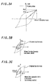
- electric field electric charge corresponding to the polarization Ps1 shown in Fig. 3A is stored in the capacitor C1 to thereby store the polarization state.
- the bit line BL and the complementary bit line /BL are discharged to the ground potential level, then subsequently, the potential of the word line WL is made to be "H" level, to thereby make the MOS transistors Q1 and Q2 ON, to start the read operation.
- the potential of the plate line PL is always the optional predetermined potential Vp.
- the MOS transistor Q1 is ON, and the voltage of the ground potential level applied to the capacitor C1, to thereby generate the electric field in the opposite direction to that of the write case between the potential Vp of the plate line PL and the capacitor C1.
- the polarization state of the ferroelectric film included therein is inverted, to inverse the storage state of polarization in the capacitor C1.
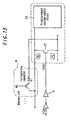
- Japanese Unexamined Patent Publication No. Hei 8-124379 discloses a semiconductor memory device in which a memory cell array 42 is provided with an erroneous write preventing circuit 41 which makes the word line WL and the bit line BL have the same potential only at the time of power on, using a power on reset circuit 40 outlined in Fig. 5.
- the power on reset circuit 40 is so constructed as to generate a power on signal PWRON which becomes "H" level for a certain period of time at the time of power on.
- a bit line potential generation circuit and an SSR circuit (not shown) are controlled to thereby control the occurrence of respective potentials (VBL, VBB and the like), and meaningless access at the time of power on is prevented by controlling stop and release of the operation of an access control circuit (not shown).
- the erroneous write preventing circuit 41 is for preventing inversion of polarization and failure of memory data in a memory cell in the ferroelectric memory cell MC with the power on signal PWRON generated by the power on reset circuit 40, and transistors Q1 and Q2 for switches are connected between at least all bit lines BL and predetermined potential nodes (Vss in the drawing).
- the MOS transistor Q becomes OFF (not connect), and external electric field is not applied to the memory retaining node of the ferroelectric capacitor C connected to the MOS transistor Q. Therefore, only polarization exists in the memory retaining node regardless of the state of the nonvolatile data, and its potential is in a floating state.
- the potential of the memory retaining node follows the potential of plate line PL and changes because of coupling of the ferroelectric capacitor. Due to the parasitic capacity of the memory retaining node, however, potential difference is caused between both ends of the capacitor C, hence there is a possibility of causing erroneous write.
- the present invention has the following construction to attain the above objects.
- a first aspect of the present invention is a semiconductor memory device comprising a matrix array of memory cells, each having a ferroelectric memory capacitor and a MOS transistor, wherein: gates of the MOS transistors in the same column are connected to the same one of a set of word lines; one of the source and the drain of the MOS transistors in the same row is connected to the same one of a set of bit lines, and the other is connected to one electrode of the memory capacitor; the other electrode of the memory capacitor is connected to a plate line; and a plurality of memory capacitors are selected in the plate line in the column direction or in the row direction; characterised in that the semiconductor memory device comprises: a gate voltage supply section which supplies a predetermined voltage to the gates of the MOS transistors connected to the word line, at the time of power on, to activate the MOS transistors and to connect the bit line and one electrode of the memory capacitor, so that the bit line and the electrode of the memory capacitor have the same potential by the MOS transistor; and a potential control section which makes the potential of the bit line and
- a second aspect of the present invention is a semiconductor memory device according to the first aspect, wherein the potential control section comprises a switching transistor for controlling conducting/non-conducting of current, and wherein by supplying predetermined voltage to the gate of the switching transistor to activate the switching transistor, the bit line and the plate line are connected so that the bit line and the plate line have the same potential.
- a third aspect of the present invention is a semiconductor memory device according to the first aspect, wherein the potential control section includes a voltage supply circuit for supplying a predetermined voltage and a switching transistor for supplying voltage from the voltage supply circuit to the bit line and/or the plate line; and wherein by supplying a predetermined voltage to the gate of the switching transistor to activate the switching transistor, the bit line and the plate line have the same potential.
- a fourth aspect of the present invention is a semiconductor memory device according to the first aspect, wherein the potential control section includes a voltage supply circuit for supplying a predetermined voltage to the bit line and the plate line, based on a power on detection signal sent out at the time of power on or at the time of returning from the power down mode, to thereby make the potential of both of the bit line and the plate line the same.
- a fifth aspect of the present invention is a semiconductor memory device according to the first aspect, wherein the potential control section formed by combining the potential control sections defined in aspect 2 to 4 is used to make the potential of the bit line and the plate line the same.
- a sixth aspect of the present invention is a semiconductor memory device according to the aspect 2 or 3, wherein the gate voltage supply section is a power on reset circuit for supplying a predetermined output voltage to at least one word line connected to the gate of the MOS transistor, at the time of power on, or for a predetermined period of time since returning from the power down mode, to activate the MOS transistor to thereby connect the bit line and the electrode of the memory capacitor, and also for supplying a predetermined output voltage to the gate of the switching transistor to activate the switching transistor to thereby make the potential of both poles of the memory capacitor the same.
- the gate voltage supply section is a power on reset circuit for supplying a predetermined output voltage to at least one word line connected to the gate of the MOS transistor, at the time of power on, or for a predetermined period of time since returning from the power down mode, to activate the MOS transistor to thereby connect the bit line and the electrode of the memory capacitor, and also for supplying a predetermined output voltage to the gate of the switching transistor to activate the switching transistor to thereby
- a seventh aspect of the present invention is a semiconductor memory device according to the aspect 4, wherein the gate voltage supply section is a power on reset circuit for supplying a predetermined output voltage to at least one word line connected to the gate of the MOS transistor, at the time of power on, or for a predetermined period of time since returning from the power down mode, to activate the MOS transistor to thereby connect the bit line and the electrode of the memory capacitor, and also for supplying a power on detection signal to the voltage supply circuit to supply predetermined voltage to the bit line and the plate line so that the potential of both lines becomes the same.
- the gate voltage supply section is a power on reset circuit for supplying a predetermined output voltage to at least one word line connected to the gate of the MOS transistor, at the time of power on, or for a predetermined period of time since returning from the power down mode, to activate the MOS transistor to thereby connect the bit line and the electrode of the memory capacitor, and also for supplying a power on detection signal to the voltage supply circuit to supply predetermined voltage to the bit line and the plate
- An eighth aspect of the present invention is a semiconductor memory device according to the aspect 6 or 7, wherein the power on reset circuit has a boosting circuit for boosting the output voltage up to the power supply voltage or higher.
- predetermined voltage is supplied to the gates of the MOS transistors connected to the word line by means of the gate voltage supply section to activate the MOS transistors, so that the bit line connected to the source or drain of the MOS transistor is connected to one electrode of the memory capacitor.
- the bit line connected to one electrode of the memory capacitor (via the MOS transistor) and the plate line connected to the other electrode thereof have the same potential.
- the potential polarity of the memory retaining node of the memory capacitor which is likely to be changed is clamped to the same potential, to thereby prevent inversion of the polarization direction of the memory capacitor at an undesirable timing, hence failure of the memory state can be prevented.
- the potential control section of the first aspect comprises a switching transistor for controlling conducting/non-conducting of current, and by supplying predetermined voltage to the gate to activate the switching transistor, the bit line and the plate line can be easily connected so that the bit line and the plate line becomes the same potential.
- the voltage control section of the first aspect includes a voltage supply circuit for supplying a predetermined voltage and a switching transistor for supplying voltage from the voltage supply circuit to the bit line and/or the plate line, and predetermined voltage is supplied to the gate of the switching transistor to activate the switching transistor.
- the bit line and the plate line have the same potential, so that at the time of power on or at the time of returning from the power down mode to the optional predetermined voltage again, inversion of the polarization direction of the memory capacitor at an undesirable timing can be prevented, to thereby prevent failure of the memory state with a simple device.
- the voltage control section of the first aspect includes a voltage supply circuit for supplying a predetermined voltage to the bit line and the plate line so as to make the potential of both lines the same, based on a power on detection signal sent out at the time of power on or at the time of returning from the power down mode, to thereby prevent inversion of the polarization direction of the memory capacitor at an undesirable timing, at the time of power on or at the time of returning from the power down mode to the optional predetermined voltage again, hence failure of the memory state can be prevented with a simple device.
- the bit line and the plate line can be made to have the same potential for general-purposes.
- predetermined output voltage is supplied to at least one word line connected to the gate of the MOS transistor, at the time of power on, or for a predetermined period of time since returning from the power down mode, to activate the MOS transistor to thereby connect the bit line and the electrode of the memory capacitor, hence the MOS transistor can be activated by a simple device utilizing the existing word line.
- the MOS transistor and the switching transistor can be activated synchronously, to make the device more efficient and controllable.
- inversion of the polarization direction of the memory capacitor at an undesirable timing can be prevented at high precision, at the time of power on or at the time of returning from the power down mode to the optional predetermined voltage again, to thereby prevent failure of the memory state.
- predetermined output voltage is supplied to at least one word line connected to the gate of the MOS transistor, at the time of power on, or for a predetermined period of time since returning from the power down mode, to activate the MOS transistor to thereby connect the bit line and the electrode of the memory capacitor, hence the MOS transistor can be activated by a simple device utilizing the existing word line.
- both electrodes of the memory capacitor can be reliably made to have the same potential, at the time of power on or at the time of returning from the power down mode to the optional predetermined voltage again, to thereby protect the memory content of the memory capacitor.
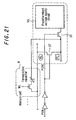
- a semiconductor memory device has a similar construction as the semiconductor memory device shown in Fig. 1, for the convenience sake of explanation, wherein a plurality of bit lines BL and a plurality of word lines WL arranged in the direction crossing the bit lines BL are arranged on a substrate, and a plurality of memory cells M are arranged in a matrix at a point corresponding to each node of the bit lines BL and the word lines WL.
- Each memory cell M is provided with at least one transistor Q (for example, MOS transistor) and at least one ferroelectric capacitor C including a ferroelectric film as an insulation film, so that the memory cells M form a nonvolatile semiconductor memory device for storing information depending upon the polarization direction of the ferroelectric film.
- the gates of the MOS transistors Q in the same column are connected to the same word line WL, and either one of the source or drain of the MOS transistors Q in the same row is connected to the same bit line BL, the other thereof is connected to one electrode of the ferroelectric capacitor C, and the other electrode of the ferroelectric capacitor C is connected to the plate line PL, so that a plurality of ferroelectric capacitors C are selected in the plate line PL.
- the semiconductor memory device comprises a power on reset circuit 5 (Fig. 7), described later, for outputting predetermined voltage until the predetermined potential becomes stable, when the predetermined potential is supplied to the bit line BL or to the plate line PL, at the time of power on or at the time of returning from the power down mode, in addition to the conventional semiconductor memory device shown in Fig. 1.
- a power on reset circuit 5 (Fig. 7), described later, for outputting predetermined voltage until the predetermined potential becomes stable, when the predetermined potential is supplied to the bit line BL or to the plate line PL, at the time of power on or at the time of returning from the power down mode, in addition to the conventional semiconductor memory device shown in Fig. 1.
- PON Fig. 7
- "H" level voltage is applied to at least one of the plurality of word lines WL shown in Fig. 6 so that the MOS transistor Q becomes ON (conductive), to thereby connect the bit line BL connected to the MOS transistor Q and the ferroelectric capacitor C.
- the power down mode stands for an operation mode in which, after power on, the plate line PL or the bit line BL supplied with the predetermined voltage is made to have optional predetermined potential for reducing the electric power consumption, regardless of being during operation or being in a standby state.
- one switching transistor ST for electrically connecting the bit line BL and the plate line PL corresponding to the memory cells M in the same row by applying predetermined potential to the gate, based on the signal PON from the power on reset circuit 5 is provided for each bit line BL and each plate line PL corresponding to the memory cells M in each row.
- the switching transistor ST is not limited to the above described arrangement, and the construction may be such that all bit lines BL and plate lines PL can be electrically connected by one switching transistor ST.
- the bit line BL and one electrode of the ferroelectric capacitor C are connected until the predetermined potential becomes stable.
- the potential of the bit line BL and the plate line of the semiconductor memory device becomes the same.
- the electric field applied to the ferroelectric capacitor C is not changed, to thereby prevent the occurrence of polarization inversion, enabling prevention of erroneous write. This will be described in more detail.
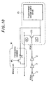
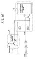
- Fig. 7 shows a circuit diagram showing the construction of the power on reset circuit 5 which outputs predetermined voltage until the predetermined potential becomes stable, when the predetermined potential is supplied to the bit line BL or plate line PL at the time of power on or at the time of returning from the power down mode, and a word line drive circuit A which applies "H" level voltage to at least one of the plurality of word lines WL, depending upon the signal PON synchronous to the output of the power on reset circuit 5.
- the word line drive circuit A in Fig. 7 is provided with a row decoder 1, an inverter 2, a level shift circuit 3 and a pair of transistors 4 in series.
- the output of the level shift circuit 3 is, respectively, connected to gate terminals of a pair of N channel transistor QN4 and P channel transistor QP4 constituting the transistor pair 4.
- the source terminal of the P channel transistor QP4 is connected to the power supply Vpp, the source terminal of the N channel transistor QN4 is connected to output-side of a pair of transistors 6 described later, and the output terminal (drain terminal) of the transistor pair 4 is connected to the word line WL.
- the power on reset circuit 5 is a signal output circuit for outputting a predetermined output voltage signal (hereinafter, this node is referred to as "POM"), until the bit line BL or the plate line PL has stable predetermined potential, at the time of power on of the device or at the time of returning from the power down mode, as described above.
- the output terminal of the power on reset circuit 5 is respectively connected to gate terminals of a pair of N channel transistor QN6 and P channel transistor QP6 constituting the transistor pair 6, respectively, via the inverter 2.
- the source terminal of the P channel transistor QP6 is connected to the power supply Vcc, the source terminal of the N channel transistor QN6 is earthed, and the output terminal (drain terminal) of the transistor pair 6 is connected to the source terminal of the N channel transistor QN4.
- the output terminal of the power on reset circuit 5 is connected to a level shift circuit 7 via two inverters 2, and the output terminal of the level shift circuit 7 is connected to a gate of the switching transistor ST described later.
- the output signal PON of the power on reset circuit 5 is time-adjusted by the two inverters 2, then changed to a predetermined potential signal of the same phase with the PON signal (hereinafter, this node is referred to as "PON1") through the level shift circuit 7 with the voltage Vpp, and used as an input signal to the switching transistor ST (Fig. 6) which makes the bit line BL and the plate line PL have the same potential, at the time of power on.
- PON1 a predetermined potential signal of the same phase with the PON signal
- the switching transistor ST Fig. 6
- two inverters are used, but the present invention is not limited thereto, or an inverter may not be used.
- the switching transistor ST can be switched ON reliably, and though not shown, the voltage applied to the word line WL is also boosted by the boosting circuit. Hence, boosting potential is supplied to the memory cell M via the word line WL, making it possible to switch the memory cell M ON reliably.
- the power on reset circuit 5 has a detection circuit which outputs an "H” signal until the predetermined potential supplied to the bit line BL or the plate line PL becomes stable, at the time of power on or returning from the power down mode which adversely affects the memory content of the ferroelectric capacitor C, and after the predetermined potential becomes stable, outputs an "L" signal.
- the "H” signal is output from the power on reset circuit 5, and the P channel transistor QP6 is switched ON by the "L” signal via the inverter 2.
- the "L" signal of the row decoder 1 is changed to an "H” signal via the inverter 2, thereby the N channel transistor QN4 is switched ON.
- the power supply Vcc is connected to the word line WL through the above described P channel transistor QP6 and the N channel transistor QN4.
- the word line WL is connected to the gate terminal of the MOS transistor Q constituting the memory cell M.
- one of the source or drain of the MOS transistor Q is connected to the bit line BL, and the other is connected to the ferroelectric capacitor C.
- Vcc supplementary power supply
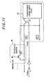
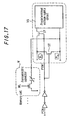
- bit line BL and the plate line PL connected to the memory cell M are connected to the source and drain of the switching transistor ST, so that on/off thereof is controlled depending upon the presence or absence of the PON1 signal voltage applied to the gate terminal. If the bit line BL and the plate line PL are electrically connected, both lines BL and PL are charged to the potential supplied from a predetermined voltage supply circuit VS to the plate line PL.
- the signal voltage PON1 in Fig. 8 is different from that shown in Fig. 7 in that it is synchronized without being through the level shift circuit 4, and an alternative circuit which does not change the voltage level is used.
- an "H” signal is output from the power on reset circuit 5, as shown in Fig. 7, until the predetermined potential supplied to the bit line BL or the plate line PL becomes stable, and the P channel transistor QP6 is switched ON by an "L” signal via the inverter 2, to thereby apply the supplementary power supply Vcc to the transistor pair 4.
- the N channel transistor QN4 is switched ON, thereby the power supply Vcc is connected to the word line WL through the above described P channel transistor QP6 and the N channel transistor QN4. Then, the supplementary power supply Vcc is applied to the gate terminal of the MOS transistor Q, for example, shown in Fig. 8, via the word line WL, hence the MOS transistor Q is ON, to thereby connect the bit line BL and the ferroelectric capacitor C.
- the signal voltage PON1 from the power on reset circuit 5 is applied to the gate of the switching transistor ST to make the switching transistor conductive, and short circuit occurs between the bit line BL and the plate line PL.
- both lines BL and PL are charged to the potential supplied from the voltage supply circuit VS to the plate line PL.
- both poles of the ferroelectric capacitor C for storing the information can be maintained to be the same potential.
- Fig. 9 shows a time chart of the power supply Vcc, predetermined supply voltage, PON signal voltage and voltage of the word line WL, in an order from up to down in the drawing.
- Time A on the time axis in the flow chart shown in Fig. 9 shows the time starting the power on
- time B shows the time when the power supply voltage and the supplied predetermined voltage become sufficiently stable, and until time B the above described PON signal is output, and the word line is "H”.
- time C is the time when the power down mode is started
- time D is the time when the supplied predetermined voltage is discharged to become the ground potential.
- Time E is the time returning from the power down mode to the operation mode
- time F is the time when the power supply voltage and the supplied predetermined voltage become sufficiently stable, and until time F the above described PON signal is output, and the word line is "H".
- "H" level voltage is applied to at least one of the plurality of word lines, to thereby connect the bit line and one electrode of the ferroelectric capacitor C, as well as when the predetermined potential is supplied to the bit line BL and the plate line PL and the like, the bit line BL and the plate line PL are connected via the switching transistor ST, thereby the bit line BL and the plate line PL become the same potential.
- both poles having the potential of the memory retaining node of the ferroelectric capacitor C which is likely to be changed are clamped to the same potential for the above described period. Thereby, inversion of the polarization direction of the ferroelectric film included in the ferroelectric capacitor C at an undesirable timing can be prevented, hence failure of the nonvolatile data stored as the polarization direction can be suppressed.
- the switching transistors ST, ST 2 are provided between the bit line BL and the plate line PL, but the switching transistors ST, ST 2 are for electrically connecting the bit line BL and the plate line PL, therefore, the switching transistors ST, ST 2 may be inserted in series between the bit line BL and the plate line PL, to connect the bit line BL and the plate line PL with the predetermined voltage supply circuit VS (see Figs. 11, 12, 17, 18, 19, 20 and 25). Furthermore, combining the above described circuits, at least two switching transistors may be provided between the bit line BL and the plate line PL (see Figs. 17 to 25).
- bit line BL and the plate line PL are directly connected by controlling ON/OFF of the switching transistor, and the case where the same voltage is applied to the bit line BL and the plate line PL from the predetermined voltage supply circuit, but it is possible to make the bit line BL and the plate line PL have the same voltage without using the switching transistor.
- a power on detection signal for example, predetermined voltage signal (PON)
- PON predetermined voltage signal
- the voltage supply circuit VS is activated (for example, the normal output is in the high impedance state, or the like), to thereby supply the same voltage to the bit line and the plate line for a predetermined period of time, hence the same effect as that of the above described embodiment can be obtained.
- a common voltage supply circuit VS is shown, but the voltage supply circuit VS may be provided separately for the bit line and the plate line.
- the bit line and the plate line may be made to have the same potential, using these device in combination. According to such a device, a device used for the general-purposes can be obtained.
- the bit line and one electrode of the memory capacitor are connected by applying "H" level voltage to at least one of the plurality of word lines, at the time of power on or at the time of returning from the power down mode, at the same time, the bit line and the plate line are connected or supplied with the predetermined potential.
- both poles of the potential of the memory retaining node of the memory capacitor which is likely to be changed are clamped to the same potential.
- inversion of the polarization direction of the ferroelectric film included in the memory capacitor at an undesirable timing can be prevented, hence failure of the nonvolatile data stored as the polarization direction can be suppressed.
- the bit line and the plate line may be directly connected, or a switching transistor for supplying voltage from the voltage supply circuit to the both lines may be used, or a voltage supply circuit for directly supplying voltage for a predetermined period of time may be used, or a simple device obtained by combining them may be used, hence failure of data in the memory capacitor can be prevented with a simple device.
- timing when the MOS transistor is activated, and timing when the potential control section is accessed to make the bit line and the plate line have the same potential can be easily controlled, hence failure of data in the memory capacitor can be prevented with a simple device.
- the gate voltage supply section and the potential control section can be reliably operated, hence failure of data in the memory capacitor can be prevented reliably.
Landscapes
- Engineering & Computer Science (AREA)
- Computer Hardware Design (AREA)
- Dram (AREA)
Claims (8)
- Halbleiterspeichervorrichtung, aufweisend eine Matrixanordnung (30) von Speicherzellen (M), von denen jede einen ferroelektrischen Speicherkondensator (C) und einen MOS-Transistor (Q) aufweist, wobei:Gates der MOS-Transistoren derselben Spalte mit derselben Wortleitung aus einem Satz an Wortleitungen (WL) verbunden sind;die Source oder Drain der MOS-Transistoren in derselben Zeile mit derselben Bitleitung aus einem Satz an Bitleitungen (BL) verbunden ist und das andere der beiden Elemente (Drain oder Source) mit einer Elektrode des Speicherkondensators verbunden ist;die andere Elektrode des Speicherkondensators mit einer Plattenleitung (PL) verbunden ist; undeine Anzahl an Speicherkondensatoren in der Plattenleitung in Spaltenrichtung oder in Reihenrichtung ausgewählt sind;dadurch gekennzeichnet, dass die Halbleiterspeichervorrichtung folgendes umfasst:einen Gatespannungs-Versorgungsabschnitt (4, 5, 6), welcher eine vorgegebene Spannung (Vcc) den Gates der MOS-Transistoren, welche mit der Wortleitung verbunden sind, zum Zeitpunkt des Einschaltens oder zum Zeitpunkt der Rückkehr aus dem Ausschaltmodus zuführt, um die MOS-Transistoren zu aktivieren und um die Bitleitung und eine Elektrode des Speicherkondensators zu verbinden, so dass die Bitleitung die Elektrode des Speicherkondensators durch den MOS-Transistor dasselbe Potenzial aufweisen; undeinen Potenzialsteuerabschnitt (ST; ST, VS; ST2, VS; ST, ST2, VS), welcher das Potenzial der Bitleitung und der Plattenleitung angleicht, so dass beide Pole des Speicherkondensators auf demselben Potenzial liegen.
- Halbleiterspeichervorrichtung nach Anspruch 1, wobei der Potenzialsteuerabschnitt einen Schalttransistor (ST) zum Steuern des Leitens/Nichtleitens von Strom aufweist und wobei durch Zuführen einer vorgegebenen Spannung zum Gate des Schalttransistors zum Aktivieren des Schalttransistors die Bitleitung und die Plattenleitung so verbunden sind, dass die Bitleitung und die Plattenleitung auf demselben Potenzial liegen.
- Halbleiterspeichervorrichtung nach Anspruch 1, wobei der Potenzialsteuerabschnitt folgendes umfasst:eine Spannungsversorgungsschaltung (VS) zum Zuführen einer vorgegebenen Spannung undeinen Schalttransistor (ST; ST2; ST, ST2) zum Zuführen von Spannung von der Spannungsversorgungsschaltung an die Bitleitung und/oder die Plattenleitung; und wobeidurch Zuführen einer vorgegebenen Spannung an das Gate des Schalttransistors zum Aktivieren des Schalttransistors die Bitleitung und die Plattenleitung auf demselben Potenzial liegen.
- Halbleiterspeichervorrichtung nach Anspruch 1, wobei der Potenzialsteuerabschnitt eine Spannungsversorgungsschaltung (VS) zum Zuführen einer vorgegebenen Spannung an die Bitleitung und die Plattenleitung basierend auf einem Einschalt-Detektionssignal, das zum Zeitpunkt des Einschaltens oder zum Zeitpunkt des Rückkehrens aus dem Ausschaltmodus ausgesendet wurde, umfasst, um hierdurch die Potenziale der Bitleitung und der Plattenleitung einander anzugleichen.
- Halbleiterspeichervorrichtung nach Anspruch 1, wobei der Potenzialsteuerabschnitt, der durch Kombinieren der Potenzialsteuerabschnitte gemäß den Ansprüchen 2 bis 4 ausgebildet ist, dazu verwendet wird, die Potenziale der Bitleitung und der Plattenleitung einander anzugleichen.
- Halbleiterspeichervorrichtung nach Anspruch 2 oder 3, wobei der Gatespannungs-Versorgungsabschnitt eine Einschalt-Resetschaltung (4, 5, 6, 7, 8) aufweist, um eine vorgegebene Ausgangsspannung (Vcc) der mindestens einer Wortleitung (WL), die mit dem Gate des MOS-Transistors verbunden ist, zum Zeitpunkt des Einschaltens oder über eine vorgegebene Zeitperiode seit der Rückkehr vom Ausschaltmodus zuzuführen, um den MOS-Transistor zu aktivieren, um hierdurch die Bitleitung und die Elektrode des Speicherkondensators miteinander zu verbinden, und
um eine vorgegebene Ausgangsspannung (PON1) dem Gate des Schalttransistors (ST) zuzuführen, um den Schalttransistor zu aktivieren, um hierdurch die Potenziale beider Pole des Speicherkondensators einander anzugleichen. - Halbleiterspeichervorrichtung nach Anspruch 4, wobei der Gatespannungs-Versorgungsabschnitt eine Einschalt-Resetschaltung (4, 5, 6, 7, 8) aufweist, um eine vorgegebene Ausgangsspannung (Vcc) mindestens einer Wortleitung (WL), die mit dem Gate des MOS-Transistors verbunden ist, zum Zeitpunkt des Einschaltens oder über eine vorgegebene Zeitperiode seit der Rückkehr aus dem Ausschaltmodus zuzuführen, um den MOS-Transistor zu aktivieren, um hierdurch die Bitzeile und die Elektrode des Speicherkondensators miteinander zu verbinden, und
um ein Einschalt-Detektionssignal der Spannungsversorgungsachaltung (VS) zuzuführen, um eine vorgegebene Spannung der Bitleitung und der Plattenleitung zuzuführen, so dass die Potenziale der beiden Leitungen einander angeglichen sind. - Halbleiterspeichervorrichtung nach Anspruch 6 oder 7, wobei die Einschalt-Resetschaltung eine Verstärkerschaltung (8) aufweist, um die Ausgangsspannung bis zur Leistungsversorgungsspannung oder darüber hinaus zu erhöhen.
Applications Claiming Priority (2)
| Application Number | Priority Date | Filing Date | Title |
|---|---|---|---|
| JP10291064A JP2000123578A (ja) | 1998-10-13 | 1998-10-13 | 半導体メモリ装置 |
| JP29106498 | 1998-10-13 |
Publications (3)
| Publication Number | Publication Date |
|---|---|
| EP0994486A2 EP0994486A2 (de) | 2000-04-19 |
| EP0994486A3 EP0994486A3 (de) | 2001-01-17 |
| EP0994486B1 true EP0994486B1 (de) | 2007-01-17 |
Family
ID=17763965
Family Applications (1)
| Application Number | Title | Priority Date | Filing Date |
|---|---|---|---|
| EP99308058A Expired - Lifetime EP0994486B1 (de) | 1998-10-13 | 1999-10-13 | Halbleiterspeicheranordnung |
Country Status (6)
| Country | Link |
|---|---|
| US (1) | US6262910B1 (de) |
| EP (1) | EP0994486B1 (de) |
| JP (1) | JP2000123578A (de) |
| KR (1) | KR100332535B1 (de) |
| DE (1) | DE69934853T2 (de) |
| TW (1) | TW442789B (de) |
Families Citing this family (20)
| Publication number | Priority date | Publication date | Assignee | Title |
|---|---|---|---|---|
| JP3971536B2 (ja) * | 1999-09-14 | 2007-09-05 | 松下電器産業株式会社 | 強誘電体メモリ装置 |
| JP3617615B2 (ja) * | 1999-11-08 | 2005-02-09 | シャープ株式会社 | 強誘電体記憶装置 |
| DE10005619A1 (de) * | 2000-02-09 | 2001-08-30 | Infineon Technologies Ag | Integrierter Halbleiterspeicher mit Speicherzellen mit ferroelektrischem Speichereffekt |
| JP3916837B2 (ja) | 2000-03-10 | 2007-05-23 | 株式会社東芝 | 強誘電体メモリ |
| JP2001291385A (ja) * | 2000-04-05 | 2001-10-19 | Nec Corp | 半導体記憶装置並びにその試験装置および試験方法 |
| DE10031947B4 (de) * | 2000-06-30 | 2006-06-14 | Infineon Technologies Ag | Schaltungsanordnung zum Ausgleich unterschiedlicher Spannungen auf Leitungszügen in integrierten Halbleiterschaltungen |
| JP2002042496A (ja) * | 2000-07-26 | 2002-02-08 | Matsushita Electric Ind Co Ltd | 強誘電体メモリ |
| JP3740577B2 (ja) * | 2001-12-20 | 2006-02-01 | 松下電器産業株式会社 | 負電位発生回路、負電位発生装置及びこれを用いた半導体装置 |
| JP3806084B2 (ja) * | 2002-12-25 | 2006-08-09 | 株式会社東芝 | 強誘電体メモリ及びそのデータ読み出し方法 |
| US7269048B2 (en) | 2003-09-22 | 2007-09-11 | Kabushiki Kaisha Toshiba | Semiconductor integrated circuit device |
| JP4672702B2 (ja) * | 2003-09-22 | 2011-04-20 | 株式会社東芝 | 半導体集積回路装置 |
| JP4074279B2 (ja) * | 2003-09-22 | 2008-04-09 | 株式会社東芝 | 半導体集積回路装置、デジタルカメラ、デジタルビデオカメラ、コンピュータシステム、携帯コンピュータシステム、論理可変lsi装置、icカード、ナビゲーションシステム、ロボット、画像表示装置、光ディスク記憶装置 |
| JP2005340356A (ja) * | 2004-05-25 | 2005-12-08 | Hitachi Ltd | 半導体記憶装置 |
| JP2007053321A (ja) * | 2005-08-19 | 2007-03-01 | Matsushita Electric Ind Co Ltd | 半導体記憶装置 |
| JP2009059398A (ja) * | 2007-08-30 | 2009-03-19 | Toshiba Corp | 強誘電体半導体記憶装置 |
| JP6148534B2 (ja) * | 2013-05-20 | 2017-06-14 | 株式会社東芝 | 不揮発性メモリ |
| US8917560B1 (en) * | 2013-11-13 | 2014-12-23 | Nanya Technology Corporation | Half bit line high level voltage genertor, memory device and driving method |
| US9590686B2 (en) | 2013-12-26 | 2017-03-07 | Google Technology Holdings LLC | Maintaining a capacitor dielectric under strain to reduce capacitance variation due to time variant hysterisis effect |
| US9715918B1 (en) * | 2016-05-23 | 2017-07-25 | Micron Technology, Inc. | Power reduction for a sensing operation of a memory cell |
| JP6625942B2 (ja) * | 2016-07-29 | 2019-12-25 | 株式会社東芝 | 半導体記憶装置 |
Family Cites Families (9)
| Publication number | Priority date | Publication date | Assignee | Title |
|---|---|---|---|---|
| JPH07111085A (ja) * | 1993-10-14 | 1995-04-25 | Sharp Corp | 不揮発性半導体記憶装置 |
| US5798964A (en) * | 1994-08-29 | 1998-08-25 | Toshiba Corporation | FRAM, FRAM card, and card system using the same |
| JP3591790B2 (ja) * | 1994-08-29 | 2004-11-24 | 東芝マイクロエレクトロニクス株式会社 | 強誘電体メモリおよびこれを用いたカードおよびカードシステム |
| JP2576425B2 (ja) * | 1994-10-27 | 1997-01-29 | 日本電気株式会社 | 強誘電体メモリ装置 |
| JP3542675B2 (ja) * | 1995-07-24 | 2004-07-14 | 株式会社ルネサステクノロジ | 半導体記憶装置 |
| US5703804A (en) * | 1996-09-26 | 1997-12-30 | Sharp Kabushiki K.K. | Semiconductor memory device |
| KR100224673B1 (ko) * | 1996-12-13 | 1999-10-15 | 윤종용 | 불휘발성 강유전체 메모리장치 및 그의 구동방법 |
| US5959878A (en) * | 1997-09-15 | 1999-09-28 | Celis Semiconductor Corporation | Ferroelectric memory cell with shunted ferroelectric capacitor and method of making same |
| KR100282045B1 (ko) * | 1998-08-07 | 2001-03-02 | 윤종용 | 강유전체 커패시터를 구비한 불 휘발성 다이나믹 랜덤 엑세스메모리 |
-
1998
- 1998-10-13 JP JP10291064A patent/JP2000123578A/ja active Pending
-
1999
- 1999-09-29 TW TW088116759A patent/TW442789B/zh not_active IP Right Cessation
- 1999-10-12 KR KR1019990044142A patent/KR100332535B1/ko not_active Expired - Fee Related
- 1999-10-13 US US09/417,274 patent/US6262910B1/en not_active Expired - Lifetime
- 1999-10-13 EP EP99308058A patent/EP0994486B1/de not_active Expired - Lifetime
- 1999-10-13 DE DE69934853T patent/DE69934853T2/de not_active Expired - Lifetime
Also Published As
| Publication number | Publication date |
|---|---|
| EP0994486A3 (de) | 2001-01-17 |
| JP2000123578A (ja) | 2000-04-28 |
| US6262910B1 (en) | 2001-07-17 |
| TW442789B (en) | 2001-06-23 |
| DE69934853T2 (de) | 2007-10-18 |
| KR20000029014A (ko) | 2000-05-25 |
| EP0994486A2 (de) | 2000-04-19 |
| KR100332535B1 (ko) | 2002-04-13 |
| DE69934853D1 (de) | 2007-03-08 |
Similar Documents
| Publication | Publication Date | Title |
|---|---|---|
| EP0994486B1 (de) | Halbleiterspeicheranordnung | |
| KR100223990B1 (ko) | 반도체 기억장치 | |
| US6587367B1 (en) | Dummy cell structure for 1T1C FeRAM cell array | |
| KR100538718B1 (ko) | 반도체기억장치 | |
| JP3431122B2 (ja) | 半導体記憶装置 | |
| KR20010030349A (ko) | 비트 라인 전압에 독립적으로 오프셋 전압을 발생시킬 수있는 반도체 메모리 장치 | |
| KR20000048350A (ko) | 센스 증폭기 회로, 이 회로를 사용한 메모리 장치, 및 이메모리 장치를 판독하는 방법 | |
| KR100275107B1 (ko) | 강유전체메모리장치및그구동방법 | |
| JP3787361B2 (ja) | 強誘電体記憶装置 | |
| US6545902B2 (en) | Ferroelectric memory device | |
| KR100323985B1 (ko) | 반도체 기억 장치 | |
| US7251153B2 (en) | Memory | |
| JP3604576B2 (ja) | 強誘電体メモリ装置 | |
| US5777934A (en) | Semiconductor memory device with variable plate voltage generator | |
| US7420833B2 (en) | Memory | |
| JP4284614B2 (ja) | 強誘電体メモリ装置 | |
| US20090059648A1 (en) | Ferroelectric semiconductor storage device | |
| US6574134B1 (en) | Non-volatile ferroelectric capacitor memory circuit having nondestructive read capability | |
| KR19980087512A (ko) | 하나의 메모리셀에 다수비트의 정보를 저장할 수 있는 반도체 기억장치 | |
| JP3568876B2 (ja) | 集積メモリおよびメモリに対する作動方法 | |
| US7177174B2 (en) | Ferroelectric memory device having a reference voltage generating circuit | |
| US6195281B1 (en) | Apparatus for generating reference voltage in ferroelectric memory device | |
| JP3593739B2 (ja) | 強誘電体記憶装置 | |
| KR19990030710A (ko) | 강유전체 메모리 장치 및 그 동작 방법 | |
| KR100373352B1 (ko) | 셀 저장노드의 전압다운 보상을 위한 저항을 갖는 강유전체 메모리 장치의 메모리 셀 |
Legal Events
| Date | Code | Title | Description |
|---|---|---|---|
| PUAI | Public reference made under article 153(3) epc to a published international application that has entered the european phase |
Free format text: ORIGINAL CODE: 0009012 |
|
| AK | Designated contracting states |
Kind code of ref document: A2 Designated state(s): DE FR GB |
|
| AX | Request for extension of the european patent |
Free format text: AL;LT;LV;MK;RO;SI |
|
| PUAL | Search report despatched |
Free format text: ORIGINAL CODE: 0009013 |
|
| AK | Designated contracting states |
Kind code of ref document: A3 Designated state(s): AT BE CH CY DE DK ES FI FR GB GR IE IT LI LU MC NL PT SE |
|
| AX | Request for extension of the european patent |
Free format text: AL;LT;LV;MK;RO;SI |
|
| RIN1 | Information on inventor provided before grant (corrected) |
Inventor name: MAEDA, KENGO Inventor name: TAKATA, HIDEKAZU |
|
| 17P | Request for examination filed |
Effective date: 20010710 |
|
| AKX | Designation fees paid |
Free format text: DE FR GB |
|
| 17Q | First examination report despatched |
Effective date: 20040820 |
|
| GRAP | Despatch of communication of intention to grant a patent |
Free format text: ORIGINAL CODE: EPIDOSNIGR1 |
|
| GRAS | Grant fee paid |
Free format text: ORIGINAL CODE: EPIDOSNIGR3 |
|
| GRAA | (expected) grant |
Free format text: ORIGINAL CODE: 0009210 |
|
| AK | Designated contracting states |
Kind code of ref document: B1 Designated state(s): DE FR GB |
|
| REG | Reference to a national code |
Ref country code: GB Ref legal event code: FG4D |
|
| REF | Corresponds to: |
Ref document number: 69934853 Country of ref document: DE Date of ref document: 20070308 Kind code of ref document: P |
|
| ET | Fr: translation filed | ||
| PLBE | No opposition filed within time limit |
Free format text: ORIGINAL CODE: 0009261 |
|
| STAA | Information on the status of an ep patent application or granted ep patent |
Free format text: STATUS: NO OPPOSITION FILED WITHIN TIME LIMIT |
|
| 26N | No opposition filed |
Effective date: 20071018 |
|
| PGFP | Annual fee paid to national office [announced via postgrant information from national office to epo] |
Ref country code: DE Payment date: 20121010 Year of fee payment: 14 Ref country code: FR Payment date: 20121018 Year of fee payment: 14 |
|
| PGFP | Annual fee paid to national office [announced via postgrant information from national office to epo] |
Ref country code: GB Payment date: 20121010 Year of fee payment: 14 |
|
| GBPC | Gb: european patent ceased through non-payment of renewal fee |
Effective date: 20131013 |
|
| REG | Reference to a national code |
Ref country code: DE Ref legal event code: R119 Ref document number: 69934853 Country of ref document: DE Effective date: 20140501 |
|
| PG25 | Lapsed in a contracting state [announced via postgrant information from national office to epo] |
Ref country code: GB Free format text: LAPSE BECAUSE OF NON-PAYMENT OF DUE FEES Effective date: 20131013 |
|
| REG | Reference to a national code |
Ref country code: FR Ref legal event code: ST Effective date: 20140630 |
|
| PG25 | Lapsed in a contracting state [announced via postgrant information from national office to epo] |
Ref country code: FR Free format text: LAPSE BECAUSE OF NON-PAYMENT OF DUE FEES Effective date: 20131031 Ref country code: DE Free format text: LAPSE BECAUSE OF NON-PAYMENT OF DUE FEES Effective date: 20140501 |