EP0996064B1 - Cellule mémoire à programmation unique - Google Patents
Cellule mémoire à programmation unique Download PDFInfo
- Publication number
- EP0996064B1 EP0996064B1 EP19990410133 EP99410133A EP0996064B1 EP 0996064 B1 EP0996064 B1 EP 0996064B1 EP 19990410133 EP19990410133 EP 19990410133 EP 99410133 A EP99410133 A EP 99410133A EP 0996064 B1 EP0996064 B1 EP 0996064B1
- Authority
- EP
- European Patent Office
- Prior art keywords
- state
- transistor
- memory cell
- programming
- cell
- Prior art date
- Legal status (The legal status is an assumption and is not a legal conclusion. Google has not performed a legal analysis and makes no representation as to the accuracy of the status listed.)
- Expired - Lifetime
Links
- 230000015654 memory Effects 0.000 title claims description 81
- 238000003860 storage Methods 0.000 claims description 38
- 238000000034 method Methods 0.000 claims description 9
- 230000006870 function Effects 0.000 claims description 6
- 238000010586 diagram Methods 0.000 description 11
- 238000004519 manufacturing process Methods 0.000 description 10
- 238000005516 engineering process Methods 0.000 description 9
- 230000003071 parasitic effect Effects 0.000 description 7
- 230000008901 benefit Effects 0.000 description 5
- 230000000694 effects Effects 0.000 description 5
- 239000002784 hot electron Substances 0.000 description 4
- 230000008569 process Effects 0.000 description 4
- 230000007423 decrease Effects 0.000 description 3
- 238000009825 accumulation Methods 0.000 description 2
- 230000004048 modification Effects 0.000 description 2
- 238000012986 modification Methods 0.000 description 2
- 229910021420 polycrystalline silicon Inorganic materials 0.000 description 2
- 230000002441 reversible effect Effects 0.000 description 2
- 101710116850 Molybdenum cofactor sulfurase 2 Proteins 0.000 description 1
- 230000004913 activation Effects 0.000 description 1
- 238000000137 annealing Methods 0.000 description 1
- 230000008033 biological extinction Effects 0.000 description 1
- 230000000903 blocking effect Effects 0.000 description 1
- 230000008859 change Effects 0.000 description 1
- 238000005520 cutting process Methods 0.000 description 1
- 230000003111 delayed effect Effects 0.000 description 1
- 238000012217 deletion Methods 0.000 description 1
- 230000037430 deletion Effects 0.000 description 1
- 238000013461 design Methods 0.000 description 1
- 238000011161 development Methods 0.000 description 1
- 230000005684 electric field Effects 0.000 description 1
- 230000005021 gait Effects 0.000 description 1
- 230000006872 improvement Effects 0.000 description 1
- 239000011159 matrix material Substances 0.000 description 1
- 244000045947 parasite Species 0.000 description 1
- 230000036316 preload Effects 0.000 description 1
- 230000009467 reduction Effects 0.000 description 1
- 230000000284 resting effect Effects 0.000 description 1
- 150000003839 salts Chemical class 0.000 description 1
- 230000001960 triggered effect Effects 0.000 description 1
Images


Classifications
-
- G—PHYSICS
- G11—INFORMATION STORAGE
- G11C—STATIC STORES
- G11C29/00—Checking stores for correct operation ; Subsequent repair; Testing stores during standby or offline operation
- G11C29/70—Masking faults in memories by using spares or by reconfiguring
- G11C29/78—Masking faults in memories by using spares or by reconfiguring using programmable devices
- G11C29/785—Masking faults in memories by using spares or by reconfiguring using programmable devices with redundancy programming schemes
- G11C29/789—Masking faults in memories by using spares or by reconfiguring using programmable devices with redundancy programming schemes using non-volatile cells or latches
-
- G—PHYSICS
- G11—INFORMATION STORAGE
- G11C—STATIC STORES
- G11C16/00—Erasable programmable read-only memories
- G11C16/02—Erasable programmable read-only memories electrically programmable
- G11C16/04—Erasable programmable read-only memories electrically programmable using variable threshold transistors, e.g. FAMOS
- G11C16/0408—Erasable programmable read-only memories electrically programmable using variable threshold transistors, e.g. FAMOS comprising cells containing floating gate transistors
- G11C16/0433—Erasable programmable read-only memories electrically programmable using variable threshold transistors, e.g. FAMOS comprising cells containing floating gate transistors comprising cells containing a single floating gate transistor and one or more separate select transistors
Definitions
- the present invention relates to the field of cells single programming memory (OTP), which are likely to keep a programmed state even after the power supply has disappeared of the circuit.
- OTP single programming memory
- the invention relates more particularly to a such a memory cell made from a MOS transistor at P channel whose grid is left floating.
- An example of application of programming cells unique is the realization of redundancy elements which are generally provided in memories produced in the form of one or several matrix networks in integrated circuit, to replace functionally a failed memory element.
- the role of single programming cells is to program the offset of columns or rows of memory when using an item redundancy to compensate for the failure of a column or of a row in the network.
- Figure 1 shows, schematically, an example of memory cell 1 with single programming of the type to which the present invention applies.
- This cell essentially consists of a P-channel MOS 2 transistor with a single gate g left floating.
- the source s of transistor 2 receives a voltage Vprog having a quiescent potential and a programming potential which will be described below.
- the transistor 2 is connected in series with a programming transistor 3, the gate of which receives a programming signal Wr and the source of which is connected to a low supply potential vss, generally the ground.
- the programming transistor 3 is an N-channel transistor whose drain is connected to the drain d of the memory transistor 2 which constitutes a storage node St carrying the stored state "0" or "1".
- each memory cell generally has two programming transistors connected in series and whose control signals vary slightly from each other. However, this distinction is not fundamental to the invention.
- a floating gate transistor memory cell uses the phenomenon, known as “electrons” hot “where, under the effect of a potential difference between the source and drain of the transistor, electrons pass through the gate oxide constituting transistor 2 and remain stored in the polycrystalline silicon grid without being able to escape, so that they fix a passing state of transistor 2 by modification apparent from its threshold voltage.
- FIGS. 2A to 2D represent, in the form of timing diagrams, an example of the pattern of signals characteristic of the memory cell.
- FIG. 2A represents the appearance of the voltage Vprog applied to the source s of the transistor 2.
- FIG. 2B represents the appearance of the programming signal Wr.
- FIG. 2C represents the shape of the voltage Vgs-Vt, where Vgs represents the gate-source voltage of transistor 2 and where Vt represents its threshold voltage.
- FIG. 2D represents the shape of the potential Vst at the storage node St.
- cell 1 is initially blank, that is to say that the storage node St is, naturally at the end of manufacture, in a "low" state due to the blocked character of transistor 2.
- the source s of transistor 2 is brought to positive potential Vdd for supplying the circuit which constitutes, for memory cell 1, a resting supply potential.
- the signal Wr remains at the low state (substantially at the potential Vss) so that the transistor 3 remains blocked. It follows that the tension Vgs-Vt is positive or zero so that the potential Vst is floating.
- the programming signal Wr is switched to the potential Vdd to make the programming transistor 3 conductive.
- the transistor 2 tends to become conductive through the strong electric field applied between its drain and its source. This results in the generation of hot electrons, some of which accumulate on its grid g . Indeed, as the potential of the source s is greater than the supply voltage Vdd (nominal), the voltage Vgs-Vt of transistor 2 ends up becoming negative so that it becomes conductive. As the gate g is isolated, these electrons cannot be evacuated and the conductive state of transistor 2 is therefore a stable state. As illustrated in FIG.
- the voltage of the storage node St begins to increase by the gradual conduction of the transistor 2.
- the storage of the electrons in the grid g causes a reduction in the threshold voltage of the transistor which is here used to make it conductive in a stable manner. It can be considered that at an instant t5, where the node St has reached the potential Vpp (by neglecting the voltage drop in the transistor 2 in the conducting state), the gate-source voltage of the transistor 2 remains stable.
- the potential of the programming signal Wr is switched towards a low state (Vss) at an instant t3 after the necessary time programming of the cell.
- Signal switching Wr intervenes after the delivery of the Vprog signal at rest (instant t1).
- the node St also passes to the potential Vdd insofar as the transistor 2 remains on. Switching the programming signal Wr after restoring the state of rest of the Vprog signal allows precisely to bring back the potential of the node St at potential Vdd.
- the voltage level Vpp necessary for programming of such a memory cell, depends on several factors among which, in particular, the duration of a programming cycle and the unitary dimension of the manufacturing technology used which also conditions the supply voltage Vdd of the circuit.
- Vpp level of around 4.5 to 5 volts is sufficient for program a cell using a floating gate transistor.
- the supply voltage Vdd nominal is around 3.3 volts.
- the rate at which hot electrons accumulate in the grid depends on the level of potential applied on the source. More specifically, the rate of accumulation of these hot electrons depends on the potential difference between the voltage applied to the source of the transistor and its voltage threshold which is related to manufacturing technology.
- Vpp voltage of approximately 4.5 volts requires a duration of approximately 100 ms to reach the stable programming of the cell, whereas a Vpp voltage of 5 volts requires only 10 ms to program the cell. It follows that the phenomenon of electron storage in the polycrystalline silicon grid of a floating gate transistor, intervenes over time without the need to apply a potential greater than the nominal supply potential on the source of this transistor.
- a disadvantage of programming memory cells unique using a floating gate transistor so is that they are likely to take a programmed state while they are only supplied by the nominal supply voltage Vdd of the circuit.
- the higher this nominal supply voltage decreases the more the deviation of the quiescent voltage of the signal Vprog by compared to the threshold voltage of the transistor decreases and more programming parasitic on food can intervene quickly.
- a floating gate cell is susceptible to be programmed parasitically by food in one year, or even less. Therefore, the necessary reliability criteria for an industrial product are, in the current state of technical, incompatible with the use of programming cells single based on insulated gate transistor.
- the document US-A-5602777 describes a memory device with base of cells made up of double gate transistors. A first grid is left floating while a second grid serves as a control grid.
- the structure of this device is a differential structure and it includes a circuit for turn off floating gate transistors after storing their content in a storage entity.
- the present invention aims to provide a cell single programming memory from a single transistor grid left floating which is compatible with low voltage Power.
- the present invention aims, in particular, to protect the memory cell of a possible parasitic programming by food.
- the present invention also aims to provide a such memory cell which remains compatible with processes CMOS transistor manufacturing classics.
- the present invention also aims to provide a space-saving solution requiring only one cell for each bit of data.
- the present invention provides a single programming memory cell comprising a single MOS transistor with single gate left floating and a means for temporarily storing the state stored by the transistor at floating gate.
- the invention also provides a memory circuit comprising memory cells organized in non-differential structure for the storage nodes of the transistors with floating gate and comprising means for fixing the instant of reading as a function of the respective time constants establishing data from programmed cells and parasitic programming of cells in the virgin state.
- the power supply to the floating gate transistor is cut in outside of periods of reading the state it memorizes, or of a cell programming period.
- temporary storage of the state stored by the transistor at floating gate is performed each time the circuit is energized in which the memory cell is integrated.
- the temporary storage means comprises a stage, for reading the state memorized by the floating gate transistor, associated with a read status storage register.
- the register is controlled, by reading the state present on at minus one input, by a signal activated when the reading stage presents a stable state on an output.
- the invention also provides a control method a memory cell of the type comprising a single transistor gate left floating, consisting in supplying the transistor with floating grid, only during reading periods of the status of the latter or during a programming period of the state of the memory cell.
- the method consists in causing the reading of the state stored in the memory cell each time the electronic circuit is powered up in which it is integrated, and to store this state in a temporary storage register.
- the same elements have been designated by the same references to the different figures. For reasons of clarity, only the elements which are necessary for the understanding of the invention have been shown in the figures and will be described by the after.
- the invention refers to a cell comprising a single gate transistor, left floating. Through Consequently, within the meaning of the invention, a floating gate transistor designates such an isolated single gate transistor (left floating).
- a memory cell according to the present invention comprises, as before, a gate P-channel MOS transistor floating, connected in series with at least one programming transistor.
- a feature of the present invention is to cut the power of the floating gate transistor outside the periods when the memory cell must be read or programmed. Thus, the periods during which the transistor at floating gate receives the positive supply voltage and thus extends the operating time before which it risks a parasitic programming of the memory cell.
- a first solution (not shown) consists in putting implementing this principle of the invention, only so functional, i.e. by applying to the gate transistor floating the positive feed potential whenever you want to read the state stored in the programming memory cell unique. If such a solution already brings an improvement compared to single programming memory cells conventional, it may prove to be insufficient in the case of memory cells whose content is read relatively often. In effect, the duration of exposure of the floating gate transistor to positive supply potential depends on the frequency with which the memory cell is addressed for reading. It follows that this solution is, in practice, limited to the realization memory cells intended to be read only very sporadically.
- a characteristic of an embodiment preferred of the present invention is to associate a transistor with floating grid to a temporary storage register, for build a protected single programming memory cell any parasitic programming by the power supply.
- the memory cell is intended to be implanted in a structure non-differential. Consequently, the invention provides for fixing the instant the cells it contains are read to guarantee obtaining reliable data despite a monostable (non-differential) system .
- the state stored in the floating gate transistor is read to be stored in the temporary register, each time energizing the circuit.
- temporary storage register for the purposes of the present invention, a register means now not the stored state when not powered.
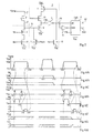
- FIG. 3 schematically shows a first embodiment of a memory cell with single programming according to the present invention.
- This cell comprises, like a conventional memory cell, a transistor 2 with a P channel and a floating g gate, connected in series with at least one programming transistor 3.
- the drain d of the transistor 2 is connected to the drain of the transistor 3 and constitutes the node St for storing the stored non-erasable data.
- the N-channel transistor 3 has its source connected to a negative supply potential Vss, generally the ground, and its gate receives a programming signal Wr from the memory cell.
- the source s of the floating gate transistor 2 is supplied by a signal Vprog whose quiescent potential corresponds to the low supply potential Vss of the circuit.
- the signal potential Vprog is brought to the high supply potential Vdd of the circuit during the periods of reading the state stored at node St, and at a programming potential Vpp exceeding the potential Vdd for programming the memory cell at a high level.
- the memory cell also includes a register 4 for temporary storage of the state memorized at node St. ce register 4 is intended to read a state occurring on a IN input on the appearance of a pulse on a control signal in reading (Sense).
- An output St 'of register 4 constitutes the output of the memory cell according to the present invention which delivers the programmed state as long as the electronic circuit, to which this memory cell is associated, is supplied with power.
- FIGS. 4A to 4F illustrate the operation of a memory cell as shown schematically in the figure 3. These figures represent, in the form of chronograms, a example of the appearance of characteristic signals of the cell during three characteristic operating phases which are the reading a blank state, programming to a high level and reading the programmed state of the cell.
- Figure 4A shows the shape of the voltage Vprog supplying the transistor to floating gate 2.
- FIG. 4B represents the shape of the signal Wr.
- FIG. 4C represents the shape of the voltage Vgs-Vt of the transistor 2.
- FIG. 4D represents the potential Vst of the node storage tank
- Figure 4E is an example of the signal shape Sense reading and FIG. 4F indicates the state St 'delivered by the temporary register 4.
- the instant t10 is chosen as a function of the time constant of node St so as to guarantee that the data read had time to settle.
- the instant t10 is later at the time of energization of a duration between the respective time constants ctmin and ctmax of node St a programmed cell and a blank cell.
- ctmin and ctmax correspond to CSt x R (2), where CSt represents the capacity of node St and where R (2) represents the resistance of the floating gate transistor 2. Note that only the latter changes significantly according to the state of the cell to be very important (tend towards infinity) in the virgin state and of the order of a hundred ohms to the programmed state.
- the time constant corresponds to the product of the capacity of the node St by the resistance in the on state of transistor 2.
- the time constant is equal to CSt x V / Ioff, where V represents the voltage across transistor 2 and where Ioff represents its leakage current in blocked state.
- the capacity of the node St is a function of the input capacity of register 4.
- the power supply of the gate transistor floating can be cut (instant t'10) as long as the non-erasable state of the cell remains available on the terminal St 'as long as the general circuit supply is not cut.
- the central part of the timing diagrams of FIGS. 4A to 4F illustrate another operating phase which corresponds to cell programming. This programming phase intervenes while the cell is blank insofar as the cell can only be electrically programmed once.
- Programming of a memory cell according to the invention is similar to programming a conventional cell as shown in Figure 1.
- a step of voltage at a programming potential Vpp on the source s of the floating gate transistor 2 instants t12, t'12, FIG. 4A.
- Vpp programming potential
- the potential Vst of the node storage is also reduced to the Vss potential. So a once programmed, the floating gate transistor 2 is no longer powered so there is no risk of programming parasitic by its food. As before, at one point t'13 posterior to instant t'12, the programming signal Wr is brought back to the low state (Vss).
- the right part of the timing diagrams of FIGS. 4A to 4F illustrates the reading, for example when switching on the circuit or after programming the cell, a cell programmed according to the invention.
- the appearance of Vprog and Sense signals is identical to that exposed in relation to the left part chronograms, that is to say with the reading of a cell Virgin.
- the potential vst follows this value and is therefore also at Vdd potential. It follows that at time t11, where the Sense signal triggers storage in register 4 of the value present on its IN input, this value is in the state high.
- register 4 memorizes this state and delivers a high state on its output St '.
- the power supply floating gate transistor 2 can be turned off so as to prevent the appearance of hot electrons and avoid thus any parasitic programming.
- An advantage of the invention is that it minimizes the periods during which the floating gate transistor is fed and, consequently, the periods during which the gate of this transistor accumulates electrons. In providing a supply for the floating gate transistor at each energization of the circuit in which the memory cell, in practice any spurious programming is prevented even for a memory cell made in a technology at low supply voltage.
- cell deletion cannot be performed electrically and requires annealing or, if necessary, a exposure to ultraviolet rays to evacuate electrons of the grid.
- Any programmable temporary storage register can be used in conjunction with a floating gate transistor to obtain a memory cell according to the invention, provided with respect the functional conditions for supplying the transistor with floating gate described above.
- FIG. 5 represents an embodiment of a memory cell of the invention illustrating an embodiment preferred of a stage 5 for reading the state stored by the transistor with floating gate 2 for its storage in a register of temporary storage 4.
- the embodiment of FIG. 5 uses the principles set out in relation to Figure 3, but shows a more detailed diagram.
- the cell of Figure 5 always includes a floating gate transistor 2 mounted in series with a programming structure.
- this programming structure consists of two N-channel MOS transistors 3 and 3 ′, connected in series between the drain d of the transistor 2 and the low supply potential Vss.
- the transistor 3 receives on its gate the programming signal Wr, while the transistor 3 'constitutes a selection transistor receiving a signal Sel on its gate.
- a programming and selection structure as shown in FIG. 5 constitutes a conventional structure for constituting, associated with a floating gate transistor, a memory cell with single programming. For a single cell, this amounts to substantially the same as the simplified structures described above.
- the selection transistor 3 ′ essentially serves for the selection of a cell to be programmed in a network of memory cells all receiving the same programming signal Wr.
- the source s of transistor 2 receives, as in the mode of previous embodiment, a power supply signal Vprog whose potential is a function of the operating phase in which is this memory cell.
- the storage node St corresponding to the drain d of the floating gate transistor 2, is connected to the input of a reading stage 5, intermediate between the transistor 2 and a storage register 4 proper.
- register 4 is supplied by potentials Vdd and Vss supplying the circuit in which the memory cell is integrated.
- This register 4 receives a signal Clk, activated, for example at the high state, to cause the memorization of the state present on its inputs not inverted IN and inverted NIN.
- Register 4 has two output terminals St 'and NSt' corresponding to the memorized state, respectively, not inverted and inverted.
- An example of temporary storage register structure 4 of this type is described, for example, in the French patent application No. 2,725,824.
- An output S5 of reading state 5 is directly connected to the IN terminal and, via an inverter 6, to the NIN terminal of register 4.
- the floor of reading 5 is a transistor assembly, suitable for reporting the state memorized at the storage node St on the entries of the register 4.
- This transistor assembly includes an N-channel transistor 7, called reader, connected between node St and low potential Vss Power.
- Transistor 7 receives a control signal Prech says read preload.
- the node St is also connected to the gate of an N-channel MOS transistor 8 whose source is connected to the potential Vss and the drain of which is connected, via two MOS transistors 9, 10 with P channel connected in series, with high supply potential Vdd.
- the common drain of transistors 8 and 10 constitute an NSt node connected, via of an inverter 11, at the output stage terminal S5 of the reading 5.
- This terminal S5 is also connected to the base of the transistor 9 and, via an N-channel transistor 12, at potential Vss.
- the base of transistor 12 receives an Init signal, said read trigger, and the base of transistor 10 receives the Ninit inverse of this Init signal.
- the NSt node constitutes, in this reading stage 5, a floating node reproducing the reverse of the state stored at node St.
- FIGS. 6A to 6H represent, in the form of chronograms, an example of gaits of characteristic signals of the diagram of FIG. 5 in three operating phases corresponding, respectively, to a reading from a blank memory cell, with a programming of this cell and a reading from the programmed memory cell.
- Figures 6A, 6B and 6C show, respectively, the pace Vprog, Wr and Sel signals.
- Figures 6D and 6E show, respectively, the appearance of the Prech and Init signals for controlling the reading stage 5.
- the Ninit signal (not shown) applied to the gate of transistor 10 corresponds to the reverse of the Init signal.
- FIG. 6F represents the signal Clk of control of the temporary storage register 4.
- FIGS. 6G and 6H represent, respectively, the potentials Vnst and Vs5 at respective nodes Nst and S5.
- the single programming cell is in a virgin state, that is to say that the transistor 2 is blocked.
- the quiescent potential of the signal Vprog is the potential Vss, so the gate transistor floating 2 is not supplied outside of periods when this is necessary for reading or programming.
- the Vprog signal is switched to the Vdd potential so that start a memory cell read cycle.
- the signals Wr and Sel are both low (Vss) since it this is not a programming cycle.
- the signal Init is switched to its rest state (Vss), which results in to block transistor 12 and, by the Ninit signal, the transistor 10.
- the Prech signal is released so that transistor 7 blocks itself.
- the drain common of transistors 8 and 10 which constitutes the node NSt is floating, that is to say it is isolated from the supply lines.
- the potential Vnst therefore remains at the potential Vdd.
- the drain of transistor 12 that is to say the node S5 remains at the low state, which is compatible with the blocking state of the transistor 12, so that the state thus read is stable to allow recording the value in the register 4.
- FIGS. 6A to 6H illustrates a programming cycle of the memory cell. This cycle is similar to that illustrated in FIGS. 4A to 4D and the Vgs-Vt and Vst voltages have not been represented again.
- FIG. 6C illustrates that the transistor 3 ′ is made conductive, at the less during the entire period t12-t'13 necessary for programming.
- the selection transistor 3 ' is made conductive by a high level (Vdd) signal Salt prior to time t12 at which the Vprog signal passes to the Vpp programming potential.
- Vdd high level
- the potential of the node St (not shown), initially forced (time t15) to potential Vss, increases towards the potential Vdd by following the form of a charge of an element capacitive so that transistor 8 turns on. he it follows that the potential Vnst goes to "0" and, by way of Consequently, the potential Vs5 goes to state "1" at the output of the inverter 11.
- the transistor 9 is then blocked so that the high state of the node NSt is stable the time to perform the memorization by the temporary register 4. We can then trigger the storage of the state at node S5 by the signal Clk.
- instant t'18 chosen to leave time 4 to store the value at node S5
- the instant t18 is delayed by a sufficient value with respect to the instant t17 to allow the signals Nst and S5 time to stabilize. This goes in the direction of guaranteeing the reliability of data read and corresponds to data compilation times at the nodes of the circuit as previously indicated. A such choice of reading instants avoids the need to a differential structure (bistable).
- register 4 The value memorized by register 4 remains present in outputs St 'and NSt' until the circuit is extinguished, i.e. until the power to register 4 is cut off.
- An advantage of the present invention is that the cell memory is protected against spurious programming by sound food.
- An advantage of saving in a register temporary, which can only change state on command by the Clk signal or in the event of loss of general power of the circuit in which the memory cell is installed, is that the reliability of the cell is made substantially independent the reading frequency of the data it stores. We however, ensure that if the cubicle is programmed of the invention, a new cycle for reading the memorized state by the floating gate transistor be triggered without waiting the next power up of the circuit.
- An advantage of reading each time voltage is that the subsequent read cycles of the circuit under voltage are not disturbed by switching the Vprog signal.
- the creation of the temporary storage register 4 is within the reach of the skilled person according to the indications functional data given above. Note that even if the register is of differential structure, the memory point St of the invention remains non-differential.
- the present invention is capable of various variants and modifications which will appear to the man of art.
- others reading periods that power up can be provided. They will, however, preferably be the most widely spaced possible.
- the respective dimensions of the different transistors used to design a programming cell unique according to the invention are within the reach of the skilled person in function of the functional constraints of this cell.
- the invention does not require a manufacturing process of particular transistor, as is the case for a EEPROM or for a double gate transistor, and is satisfied with a CMOS process.
Landscapes
- Engineering & Computer Science (AREA)
- Microelectronics & Electronic Packaging (AREA)
- Read Only Memory (AREA)
Description
Claims (6)
- Cellule mémoire à programmation unique du type comportant un seul transistor MOS à simple grille, laissée flottante (2), caractérisée en ce qu'elle comporte un moyen (4) de mémorisation temporaire de l'état stocké par le transistor à grille flottante, l'alimentation du transistor à grille flottante (2) étant coupée en dehors de périodes (t10, t'10) de lecture de l'état qu'il mémorise, ou d'une période de programmation (t12, t'12) de la cellule.
- Cellule mémoire selon la revendication 1, caractérisée en ce que la mémorisation temporaire de l'état stocké par le transistor à grille flottante (2) est effectuée à chaque mise sous tension du circuit dans lequel est intégrée la cellule mémoire.
- Cellule mémoire selon la revendication 1 ou 2, caractérisée en ce que le moyen de stockage temporaire comporte un étage (5), de lecture de l'état mémorisé par le transistor à grille flottante (2), associé à un registre (4) de stockage de l'état lu.
- Cellule mémoire selon la revendication 3, caractérisée en ce que le registre (4) est commandé, en lecture de l'état présent sur au moins une entrée (IN, NIN), par un signal (Clk) activé lorsque l'étage de lecture (5) présente un état stable sur une sortie (S5).
- Circuit mémoire comprenant des cellules mémoire conformes à l'une quelconque des revendications 1 à 4, caractérisé en ce qu'il comporte des moyens propres à fixer un instant de lecture des états respectifs stockés par les cellules pour mémorisation temporaire, en fonction des constantes de temps respectives des cellules selon leur état vierge ou programmé.
- Procédé de commande d'une cellule mémoire du type comportant un seul transistor à simple grille, laissée flottante (2), caractérisé en ce qu'il consiste :à alimenter le transistor à grille flottante, uniquement pendant des périodes de lecture (t10, t'10) de l'état de ce dernier ou pendant une période de programmation (t12, t'12) de l'état de la cellule mémoire ;à provoquer la lecture de l'état stocké dans la cellule mémoire à chaque mise sous tension du circuit électronique dans lequel elle est intégrée, et à stocker cet état dans un registre (4) de mémorisation temporaire, l'instant de lecture étant choisi postérieurement à l'instant de mise sous tension d'une durée supérieure au temps d'établissement de l'état d'une cellule programmée et inférieure à la constante de temps d'une cellule à l'état vierge.
Applications Claiming Priority (2)
| Application Number | Priority Date | Filing Date | Title |
|---|---|---|---|
| FR9813168A FR2784783B1 (fr) | 1998-10-16 | 1998-10-16 | Cellule memoire a programmation unique |
| FR9813168 | 1998-10-16 |
Publications (2)
| Publication Number | Publication Date |
|---|---|
| EP0996064A1 EP0996064A1 (fr) | 2000-04-26 |
| EP0996064B1 true EP0996064B1 (fr) | 2003-12-17 |
Family
ID=9531798
Family Applications (1)
| Application Number | Title | Priority Date | Filing Date |
|---|---|---|---|
| EP19990410133 Expired - Lifetime EP0996064B1 (fr) | 1998-10-16 | 1999-10-13 | Cellule mémoire à programmation unique |
Country Status (3)
| Country | Link |
|---|---|
| EP (1) | EP0996064B1 (fr) |
| DE (1) | DE69913640D1 (fr) |
| FR (1) | FR2784783B1 (fr) |
Families Citing this family (2)
| Publication number | Priority date | Publication date | Assignee | Title |
|---|---|---|---|---|
| WO2004040579A1 (fr) * | 2002-08-22 | 2004-05-13 | Thomson Licensing S.A. | Registre de carte a puce a ecriture seule |
| US8320191B2 (en) | 2007-08-30 | 2012-11-27 | Infineon Technologies Ag | Memory cell arrangement, method for controlling a memory cell, memory array and electronic device |
Family Cites Families (3)
| Publication number | Priority date | Publication date | Assignee | Title |
|---|---|---|---|---|
| US3744036A (en) * | 1971-05-24 | 1973-07-03 | Intel Corp | Electrically programmable read only memory array |
| JP3160160B2 (ja) * | 1994-09-28 | 2001-04-23 | シャープ株式会社 | 半導体記憶装置 |
| JPH1116387A (ja) * | 1997-06-26 | 1999-01-22 | Mitsubishi Electric Corp | 冗長回路 |
-
1998
- 1998-10-16 FR FR9813168A patent/FR2784783B1/fr not_active Expired - Fee Related
-
1999
- 1999-10-13 EP EP19990410133 patent/EP0996064B1/fr not_active Expired - Lifetime
- 1999-10-13 DE DE69913640T patent/DE69913640D1/de not_active Expired - Lifetime
Also Published As
| Publication number | Publication date |
|---|---|
| DE69913640D1 (de) | 2004-01-29 |
| FR2784783A1 (fr) | 2000-04-21 |
| FR2784783B1 (fr) | 2001-11-02 |
| EP0996064A1 (fr) | 2000-04-26 |
Similar Documents
| Publication | Publication Date | Title |
|---|---|---|
| EP0080394B1 (fr) | Bascule bistable à stockage non volatil et à repositionnement statique | |
| EP0666573B1 (fr) | Bascule bistable non volatile programmable par la source, notamment pour circuit de redondance de mémoire | |
| EP1434237B1 (fr) | Cellule de mémoire SRAM non volatile | |
| FR2480504A1 (fr) | Transistor programmable et effacable electriquement | |
| EP1014447A1 (fr) | Cellule mémoire à programmation unique en technologie CMOS | |
| FR2778012A1 (fr) | Dispositif et procede de lecture de cellules de memoire eeprom | |
| EP0718849A1 (fr) | Procédé d'écriture de données dans une mémoire et mémoire électriquement programmable correspondante | |
| EP0279712B1 (fr) | Circuit de lecture pour mémoire | |
| FR2957449A1 (fr) | Micro-amplificateur de lecture pour memoire | |
| EP0278832B1 (fr) | Circuit de lecture pour mémoire | |
| FR2775382A1 (fr) | Procede de controle du rafraichissement d'un plan memoire d'un dispositif de memoire vive dynamique, et dispositif de memoire vive correspondant | |
| FR2762708A1 (fr) | Procede de commande d'une cellule memoire et memoire non volatile programmable une seule fois en technologie cmos | |
| EP0996064B1 (fr) | Cellule mémoire à programmation unique | |
| FR2871282A1 (fr) | Dispositif memoire programmable une seule fois | |
| FR2770326A1 (fr) | Procede d'ecriture dans une memoire non volatile modifiable electriquement | |
| FR2751778A1 (fr) | Memoire accessible en lecture seulement | |
| EP1158408B1 (fr) | Mémoire EEPROM comprenant un système de correction d'erreur | |
| FR2897193A1 (fr) | Circuit de fusible electrique procurant une fonction de lecture de marge | |
| EP1486987A1 (fr) | Memoire flash comprenant des moyens de contrôle et de rafraíchissement de cellules mémoire dans l'état effacé | |
| EP2977988B1 (fr) | Mémoire non volatile à résistance programmable | |
| EP1168359B1 (fr) | Procédé de commande d'un accès en lecture d'une mémoire vive dynamique et mémoire correspondante. | |
| EP3518241B1 (fr) | Mémoire sram à déclenchement de fin de lecture améliorée | |
| EP1164592A1 (fr) | Dispositif de mémoire vive dynamique et procédé de commande d'un accès en lecture d'une telle mémoire | |
| EP0478440B1 (fr) | Circuit de précharge pour la lecture de mémoires | |
| EP1103979A1 (fr) | Dispositif de mémoire vive dynamique, et procédé de lecture correspondant |
Legal Events
| Date | Code | Title | Description |
|---|---|---|---|
| PUAI | Public reference made under article 153(3) epc to a published international application that has entered the european phase |
Free format text: ORIGINAL CODE: 0009012 |
|
| AK | Designated contracting states |
Kind code of ref document: A1 Designated state(s): DE FR GB IT |
|
| AX | Request for extension of the european patent |
Free format text: AL;LT;LV;MK;RO;SI |
|
| 17P | Request for examination filed |
Effective date: 20001019 |
|
| AKX | Designation fees paid |
Free format text: DE FR GB IT |
|
| RAP1 | Party data changed (applicant data changed or rights of an application transferred) |
Owner name: STMICROELECTRONICS S.A. |
|
| 17Q | First examination report despatched |
Effective date: 20020906 |
|
| GRAH | Despatch of communication of intention to grant a patent |
Free format text: ORIGINAL CODE: EPIDOS IGRA |
|
| RIN1 | Information on inventor provided before grant (corrected) |
Inventor name: JACQUET, FRANEOIS Inventor name: FERRANT, RICHARD |
|
| GRAS | Grant fee paid |
Free format text: ORIGINAL CODE: EPIDOSNIGR3 |
|
| GRAA | (expected) grant |
Free format text: ORIGINAL CODE: 0009210 |
|
| AK | Designated contracting states |
Kind code of ref document: B1 Designated state(s): DE FR GB IT |
|
| PG25 | Lapsed in a contracting state [announced via postgrant information from national office to epo] |
Ref country code: IT Free format text: LAPSE BECAUSE OF FAILURE TO SUBMIT A TRANSLATION OF THE DESCRIPTION OR TO PAY THE FEE WITHIN THE PRESCRIBED TIME-LIMIT;WARNING: LAPSES OF ITALIAN PATENTS WITH EFFECTIVE DATE BEFORE 2007 MAY HAVE OCCURRED AT ANY TIME BEFORE 2007. THE CORRECT EFFECTIVE DATE MAY BE DIFFERENT FROM THE ONE RECORDED. Effective date: 20031217 |
|
| REG | Reference to a national code |
Ref country code: GB Ref legal event code: FG4D Free format text: NOT ENGLISH |
|
| REF | Corresponds to: |
Ref document number: 69913640 Country of ref document: DE Date of ref document: 20040129 Kind code of ref document: P |
|
| PG25 | Lapsed in a contracting state [announced via postgrant information from national office to epo] |
Ref country code: DE Free format text: LAPSE BECAUSE OF FAILURE TO SUBMIT A TRANSLATION OF THE DESCRIPTION OR TO PAY THE FEE WITHIN THE PRESCRIBED TIME-LIMIT Effective date: 20040318 |
|
| GBT | Gb: translation of ep patent filed (gb section 77(6)(a)/1977) |
Effective date: 20040301 |
|
| PLBE | No opposition filed within time limit |
Free format text: ORIGINAL CODE: 0009261 |
|
| STAA | Information on the status of an ep patent application or granted ep patent |
Free format text: STATUS: NO OPPOSITION FILED WITHIN TIME LIMIT |
|
| 26N | No opposition filed |
Effective date: 20040920 |
|
| PGFP | Annual fee paid to national office [announced via postgrant information from national office to epo] |
Ref country code: FR Payment date: 20050825 Year of fee payment: 7 |
|
| PGFP | Annual fee paid to national office [announced via postgrant information from national office to epo] |
Ref country code: GB Payment date: 20060926 Year of fee payment: 8 |
|
| REG | Reference to a national code |
Ref country code: FR Ref legal event code: ST Effective date: 20070629 |
|
| PG25 | Lapsed in a contracting state [announced via postgrant information from national office to epo] |
Ref country code: FR Free format text: LAPSE BECAUSE OF NON-PAYMENT OF DUE FEES Effective date: 20061031 |
|
| GBPC | Gb: european patent ceased through non-payment of renewal fee |
Effective date: 20071013 |
|
| PG25 | Lapsed in a contracting state [announced via postgrant information from national office to epo] |
Ref country code: GB Free format text: LAPSE BECAUSE OF NON-PAYMENT OF DUE FEES Effective date: 20071013 |