EP0996143A2 - Procédé de réduction des erreurs de positionnement des motifs en lithographie par faisceau électronique par projection - Google Patents
Procédé de réduction des erreurs de positionnement des motifs en lithographie par faisceau électronique par projection Download PDFInfo
- Publication number
- EP0996143A2 EP0996143A2 EP99121177A EP99121177A EP0996143A2 EP 0996143 A2 EP0996143 A2 EP 0996143A2 EP 99121177 A EP99121177 A EP 99121177A EP 99121177 A EP99121177 A EP 99121177A EP 0996143 A2 EP0996143 A2 EP 0996143A2
- Authority
- EP
- European Patent Office
- Prior art keywords
- electron
- lens system
- section
- electronic
- wafer
- Prior art date
- Legal status (The legal status is an assumption and is not a legal conclusion. Google has not performed a legal analysis and makes no representation as to the accuracy of the status listed.)
- Withdrawn
Links
Images




Classifications
-
- H—ELECTRICITY
- H01—ELECTRIC ELEMENTS
- H01J—ELECTRIC DISCHARGE TUBES OR DISCHARGE LAMPS
- H01J37/00—Discharge tubes with provision for introducing objects or material to be exposed to the discharge, e.g. for the purpose of examination or processing thereof
- H01J37/02—Details
- H01J37/04—Arrangements of electrodes and associated parts for generating or controlling the discharge, e.g. electron-optical arrangement or ion-optical arrangement
- H01J37/147—Arrangements for directing or deflecting the discharge along a desired path
- H01J37/1471—Arrangements for directing or deflecting the discharge along a desired path for centering, aligning or positioning of ray or beam
-
- B—PERFORMING OPERATIONS; TRANSPORTING
- B82—NANOTECHNOLOGY
- B82Y—SPECIFIC USES OR APPLICATIONS OF NANOSTRUCTURES; MEASUREMENT OR ANALYSIS OF NANOSTRUCTURES; MANUFACTURE OR TREATMENT OF NANOSTRUCTURES
- B82Y10/00—Nanotechnology for information processing, storage or transmission, e.g. quantum computing or single electron logic
-
- H—ELECTRICITY
- H01—ELECTRIC ELEMENTS
- H01J—ELECTRIC DISCHARGE TUBES OR DISCHARGE LAMPS
- H01J2237/00—Discharge tubes exposing object to beam, e.g. for analysis treatment, etching, imaging
- H01J2237/15—Means for deflecting or directing discharge
- H01J2237/1504—Associated circuits
-
- H—ELECTRICITY
- H01—ELECTRIC ELEMENTS
- H01J—ELECTRIC DISCHARGE TUBES OR DISCHARGE LAMPS
- H01J2237/00—Discharge tubes exposing object to beam, e.g. for analysis treatment, etching, imaging
- H01J2237/153—Correcting image defects, e.g. stigmators
-
- H—ELECTRICITY
- H01—ELECTRIC ELEMENTS
- H01J—ELECTRIC DISCHARGE TUBES OR DISCHARGE LAMPS
- H01J2237/00—Discharge tubes exposing object to beam, e.g. for analysis treatment, etching, imaging
- H01J2237/30—Electron or ion beam tubes for processing objects
- H01J2237/317—Processing objects on a microscale
- H01J2237/3175—Lithography
- H01J2237/31761—Patterning strategy
- H01J2237/31764—Dividing into sub-patterns
Definitions
- This invention relates generally to projection electron-beam lithography systems. More specifically this invention relates to a technique to reduce pattern placement errors in projection electron-beam lithography systems.
- One such technique utilizes an electron-beam lithography system in which electrons are directed onto the surface of a semiconductor wafer to expose an electron sensitive resist coating on the surface of the semiconductor wafer. After exposure and development, the resulting resist pattern is used as a template to effect patterned modifications on or to the underlying semiconductor material.
- the classic electron-beam lithography system is the "probe-forming" system in which a narrow beam of electrons that is the image of the electron source and having a Gaussian distribution is scanned over the surface to be exposed.
- the narrow beam is scanned a pixel at a time, the pixel being defined as the full width at half height of the beam intensity distribution.
- These systems can have the highest spatial resolution, but also have the lowest throughput of all electron-beam lithography systems due to the serial exposure of patterns one pixel at a time.
- One advantage of systems that serially expose patterns is that corrections can be applied dynamically, pixel by pixel, to compensate for aberrations of the electron lenses and deflection units in the system.
- Another advantage is that if the pixel represents the smallest feature of the desired pattern, a pattern of any arbitrary complexity can be created with this type of probe.
- a further advantage is that proximity corrections are also easily made with this type of probe.
- Electron-beam lithography systems with this feature create a shaped spot on the wafer by generating an image of apertures or other objects illuminated by the source, that is, not an image of the source itself.
- the image is electronically variable in size and adjustable to compose a pattern feature with serial exposures projecting up to several hundred pixels in parallel.
- An increase in throughput can also be achieved by providing a mask (reticle) through which a beam of electrons is directed and electronically focused onto the surface of the semiconductor wafer.
- the reticle has a pattern formed thereon that describes the features of the circuit or structure that is to be formed on the semiconductor wafer. Because the size of the reticle far exceeds the field of view of the electronic lenses that are available, it is necessary to direct the electron beam onto a portion of the reticle and then move (step or scan) the electron beam sequentially to other portions of the reticle.
- the reticle is divided into subfields and each subfield is illuminated one at a time by sequentially stepping or scanning the electron beam from one subfield to the next until the pattern on the reticle has been completely transferred by an electronic projection lens system onto the surface of the semiconductor wafer.
- the reticle may be moved so that other portions of the reticle are sequentially illuminated by the electron beam.
- the present invention overcomes the above problems and provides other additional advantages through electron-beam lithography systems that transfer images from subfields in a reticle to a semiconductor wafer and that position electron beams emerging from the subfields onto a semiconductor wafer with an accuracy in the range of 1 nanometer.
- deflection systems in the electronic lens system in the electron-beam lithography systems are controlled by inputs switched by first and second switches and position errors in the inputs are corrected by inputs from error tables.
- the deflection systems can either deflect electron beams emerging from subfields in the reticle to coincide with an electronic optical axis or deflect the electronic optical axis to coincide with the electron beams.
- the input from the first switch either deflects the electron beams or the electronic optical axis to within a range R R in accordance with the following condition:
- the input from the second switch either deflects the electron beams or the electronic optical axis to within a range R w in accordance with the following condition:
- a ⁇ 2 B R w , where R w is the range within which the input from the first switch is designed to deflect either the electron beams or the electronic optical axis.
- the desired accuracy of the electron-beam lithography system is in the range of 0.5 to 100 nanometers and the accuracy of the error DACs is in the range of 8 bits to 18 bits.
- deflection systems in the electronic lens system in electron-beam lithography systems are controlled by inputs from a main DAC.
- the output of the main DAC is amplified by a first amplifier with a gain G 1 and input to a first deflection system that either deflects electron beams emerging from subfields in the reticle to coincide with an electronic optical axis or deflects the electronic optical axis to coincide with the electron beams.
- the output of the main DAC is amplified by a second amplifier with a gain G 2 and input to a second deflection system that either deflects electron beams to coincide with the electronic optical axis or deflects the electronic optical axis to coincide with the electron beams.
- the electronic lens system is insensitive to position errors in the main DAC when the following condition is satisfied:
- G 1 /G2 M, where M is the magnification of the electronic lens system.
- inputs are summed with inputs from a grillage error DAC that has inputs from an error table.
- the sum is amplified by a third amplifier and the output of the third amplifier is summed with the output of the first amplifier and input to the first deflection system.
- deflection systems in the electronic lens system in electron-beam lithography systems are controlled by an input from a ramp generator with an output that is amplified by a first amplifier having a gain G 1 and input to a first deflection system that either deflects electron beams emerging from subfields in the reticle to coincide with an electronic optical axis or deflects the electronic optical axis to coincide with the electron beams.
- the output of the ramp generator is amplified by a second amplifier with a gain G 2 and input to a second deflection system that either deflects the electron beams to coincide with the electronic optical axis or deflects the electronic optical axis to coincide with the electron beams.
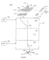
- Figure 1 illustrates a portion of a projection electron-beam lithography system 100 showing a portion of a reticle 102 , an electronic lens system 104 and a portion of a semiconductor wafer 106 .
- the reticle 102 is divided into subfields such as those indicated at 108 .
- the subfields 108 have been given a notation of " nm " where " n " is the number of rows and " m " is the number of columns.
- the first subfield 110 is then denoted as 11 and the last subfield 112 in the first row would be denoted as 1m and the last subfield 114 in the first column would be denoted as n1 .
- the last subfield 116 in the last row and last column would be denoted as nm .
- the subfields 108 can be separated by "grillage" that are extra bars of blank material between the subfields.
- the columnar grillage " g " is shown at 118 and the grillage separating the rows is shown at 120 . It is noted that the columnar grillage can be different than the row grillage.
- the width " a " of the subfields is shown at 122 and the height " b “ of the subfields is shown at 124 .
- the width " a " and the height " b " can be equal or different.
- Typical values for the width and height is 1 millimeter and for the grillage is 0.3 millimeters. It should be appreciated that other widths and heights and grillage values can be used and the use of 1 millimeter for width and height and 0.3 millimeters for the grillage are for illustrative purposes only.
- FIG. 1 there is shown a representation of an electron beam 126 emerging from a subfield n2 of the reticle 102 and entering the electronic lens system 104 .
- a first section 128 of the electronic lens system 104 includes a deflection system that deflects the electron beam 126 emerging from the reticle 102 to coincide with the electronic optical axis 130 ofthe electronic lens system 104 .
- a second section 132 of the electronic lens system 104 includes a magnification lens system that demagnifies the beam 126 emerging from the first section 128 of the electronic lens system 104 .
- a third section 134 ofthe electronic lens system 104 includes a deflection system that deflects the demagnified beam 126 emerging from the second section 132 of the electronic lens system 104 to the appropriate region on the wafer 106 . It should be appreciated that the magnification section 132 can be coincident with one or both of the deflection sections 128 and 134 .
- the gain of the magnification lens system in the second section 132 typically has a value of-1/M where M is typically a value such as 4.
- M typically a value such as 4.
- the minus indicates that the image is inverted from top to bottom and from right to left. Therefore, the image on the wafer 106 is inverted from top to bottom and from right to left.
- the deflection system in section 128 of the electronic lens system 104 can be controlled by a DAC (Digital to Analog Converter) 136 and the deflection lens system in section 134 of the electronic lens system 104 can also be controlled by a DAC 138 .
- the various components are further controlled by a central processing unit (cpu) not shown. Such a cpu would coordinate the functions described above. Such a unit is not part of the present invention and will not be shown or discussed.
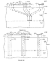
- Figure 2A illustrates a portion 200 of the projection electron-beam lithography system 100 shown in Figure 1 .
- Subfields of the reticle 102 are shown at 202, 204, 206, 208 , and 210.
- the grillage between the subfields 202, 204, 206, 208 , and 210 are shown at 212, 214, 216, 218 and 220 .
- a beam of electrons 222 is shown being directed onto the subfield 208 .
- a projection electron-beam lithography system has a source of electrons that emits a beam of electrons that is shaped by an electronic shaping system (not shown) into a collimated electron beam that is slightly larger than the subfields that are to be illuminated by the electron beam.
- An electronic deflection system (not shown) then sequentially deflects the shaped electron beam onto the appropriate subfield.
- the electron beam 222 is moved from subfield to subfield, typically from a first end of a row to the second end of the row at which time the electron beam can either be returned to the first end of the next row until all the rows have been illuminated or the electron beam can describe a serpentine path through the successive rows, that is, when one row is finished, the electron beam is stepped to the next row and is moved in the opposite direction until all the rows have been illuminated.
- any other illumination pattern of the reticle can be used.
- the reticle may be moved so that subfields on the reticle are being illuminated by the shaped electron beam.
- the electron beam 224 emerging from the subfield 202 is deflected by the deflection system 128 to the electronic optical axis 130 of the electronic lens system 104 .
- the electron beam from each of the subfields it is necessary for the electron beam from each of the subfields to be deflected to the electronic optical axis 130 of the electronic lens system 104 in order to minimize aberrations and distortion of the electron beam emerging from each of the subfields on the reticle 102 .
- the aberrations and distortion of the electron beam typically increase if the electron beam is not centered on the electronic optical axis 130 of the electronic lens system 104 .
- the electron beams 226 and 228 emerging from subfields 208 and 210 respectively, must be accurately deflected to be centered on the electronic optical axis 130 of the electronic lens system 104 .
- Figure 2B illustrates a portion 230 of a projection electron-beam lithography system similar to the one shown in Figure 1 .
- the portion 230 of the projection electron-beam lithography system shows the subfields of the reticle 102 at 202, 204 , 206, 208 and 210 .
- the grillage between the subfields 202, 204, 206, 208 and 210 are shown at 212, 214, 216, 218 and 220 .
- a beam of electrons 222 is shown being directed onto the subfield 208 .
- the beam of electrons 226 emerging from the subfield 208 is shown coincident with the electronic optical axis 130 .
- the electronic optical axis 130 is moved to be coincident with the electron beam 224 emerging from the subfield 202 .
- the electronic optical axis 130 is moved to be coincident with the electron beam 228 emerging from the subfield 210 and the other subfields.
- Figure 3A illustrates a portion 300 of the projection electron-beam lithography system 200 shown in Figure 2A .
- Three subfields 302, 304 , and 306 of the reticle 102 are shown with electron beams 308, 310 and 312 emerging from the subfields 302, 304 , and 306 , respectively.
- Each of the electron beams 308, 310 and 312 have a centerline 314, 316 and 318 , respectively.
- each of the centerlines 314, 316 and 318 of the electron beams 308, 310 , and 312 respectively, coincide with the electronic optical axis 130 of the projection lens system 104 .
- the centerline 314 of electron beam 308 is shown misaligned with the electronic optical axis 130 of the projection lens system 104 .
- the amount of the misalignment is shown at 320 .
- the centerlines 316 and 318 of electron beams 310 and 312 are shown misaligned with the electronic optical axis 130 of the projection lens system 104 .
- the misalignment of centerline 316 is shown at 322 and the misalignment of centerline 318 is shown at 324 .
- each of the beams emerging from each subfield in the reticle may have misalignments that must be corrected.
- Figure 3B illustrates a portion 326 of a projection electron-beam lithography system similar to the projection electron-beam lithography system 200 shown in Figure 2B .
- the difference between the portion 326 shown in Figure 3B and the portion 300 shown in Figure 3A is that the portion 326 shown in Figure 3B shows the electronic optical axis 130 being deflected to coincide with the centerlines of the electron beams emerging from the subfields in the reticle 102 .
- Three subfields 302 , 304 and 306 of the reticle 102 are shown with electron beams 308, 310 and 312 emerging from the subfields 302, 304 and 306 respectively.
- Each of the electron beams 308, 310 and 312 have a centerline 314, 316 and 318 , respectively.
- each of the centerlines 314, 316 , and 318 coincide with the electronic optical axis 130 of the projection lens system 104 .
- the electronic optical axis 130 is shown misaligned with the centerline 314 of the electron beam 308 . The amount of the misalignment is shown at 328 .
- the electronic optical axis 130 is shown misaligned with the ceriterlines 316 and 318 of electron beams 310 and 312 , respectively.
- the misalignment of the electronic optical axis 130 with the centerline 316 is shown at 330 and the misalignment of the electronic optical axis 130 with the centerline 318 is shown at 332 .
- the electronic optical axis 130 may be misaligned with the electron beams emerging from each of the subfields in the reticle and that misalignment must be corrected to minimize the aberrations and distortion of the electron beams.
- Figure 4 shows a row of 20 subfields that could be found in a typical reticle. It should be appreciated that the number of subfields in a row can be a number other than 20. For purposes of illustration and discussion, there are shown 20 subfields having a width "a,” a grillage “g” and a pitch "p" that is equal to (a + g). In order to have a specified accuracy for a given number of subfields as shown in Figure 4 , the number of bits required to control the DAC that control the deflection systems can be calculated from the following:
- a system with a 0.25 by 0.25 millimeter field size at the wafer, 1/4X magnification, 100 ⁇ A beam current at the reticle, a 25 ⁇ m beam current at the wafer (25% reticle transmission) and 5 ⁇ C/cm 2 resist sensitivity requires an exposure time of 32 ⁇ sec per subfield. This indicates the potential throughput drops in half if the DAC settling time is as long as 32 ⁇ sec. A typical requirement for the settling time may be less than 25 ⁇ sec.
- a typical electron-beam lithography system might have a 5 millimeter wide deflection at the wafer in one direction, thus dividing the scan area into 20 subfields (5mm/0.25mm) that must be scanned accurately.
- the reticle scan DACs For a 1 nanometer accuracy at the wafer and a 4 nanometer accuracy at the reticle, the reticle scan DACs must have at least approximately a 23 bit scan accuracy log 2 (24.7mm/4nm) ⁇ 22+ bits, which is rounded to 23 bits.
- 23 bit, 25 ⁇ sec DACs are not presently commercially available.
- the device 500 includes the electronic lens system 104 , a first control section 501 comprising a first switch 502 and a first error DAC 504 that control the operation of a deflection system in the first section 128 of the electronic lens system 104 .
- the first switch 502 switches between first sources S 1 through S m 503 .
- the first sources 503 may be current sources or voltage sources.
- the m first sources coincide with the m subfields, for example, the first switch 502 switches to first source S 1 when the first subfield in a row is being illuminated and switches to first source S 2 when the second subfield in a row is being illuminated and so on until all subfields in a row have been illuminated.
- the device 500 also includes a second control section 505 comprising a second switch 506 and a second error DAC 508 that control the operation of a deflection system in the third section 134 of the electronic lens system 104 .
- the second switch 506 switches between second sources S 1 through S m 507 .
- the second sources 507 may be current sources or voltage sources.
- the centerline 510 of the electron beam emerging from the subfield 302 may be misaligned from the electronic optical axis 130 as indicated at 512 due in part to a positioning error in the relevant first source 503 .
- the path 511 is the desired path for the centerline 510 of the electron beam.
- each of the electron beams that emerge from each of the subfields in the reticle 102 may each have a unique misalignment or alignment error and it is necessary that the device 500 be capable of correcting each of the misalignment errors as the electron beam is moved from subfield to subfield.
- the required accuracy of the first sources S 1 503 and the second sources S 2 507 and the error DACs 504 & 508 will be discussed below.
- the first sources S 1 503 cause the centerlines of the electron beams such as the centerline 510 of the electron beam to be deflected towards the electronic optical axis 130 .
- the second sources S 2 cause the centerlines of the electron beams to be deflected to the appropriate region on the wafer 106 . If there is a misalignment or alignment error as indicated at 512 the first error DAC 504 supplies a signal to correct the misalignment so that the centerline 510 of the electron beam coincides with the electronic optical axis 130 .
- the second error DAC 508 supplies a signal to correct the misalignment or alignment error.
- the first and second error DACs 504 & 508 generate a correction signal from Tables 514 & 516 , respectively, which have error data 518 tabulated for each subfield.
- the error data 518 is generated by running a calibration reticle through the lithography system and observing and tabulating the errors.
- a major requirement of the first sources 503 and the second sources 507 is that they are consistent in the amount of misalignment for each subfield.
- the misalignment for a given subfield in each row must be the same each time that subfield in each row is illuminated by the electron beam.
- the signal from each of the first sources S 1 through S m 503 and from each of the second sources S 1 through S m 507 is summed at 520 & 522 with the signal from the error DACs 504 & 508 , respectively.
- the summed signals then control the deflection system in the first section 128 of the electronic lens system 104 and in the second section 134 of the electronic lens system 104 . If there are 20 subfields in a row, there will be 20 first sources that are sequentially switched by switch 502 corresponding to the subfield being illuminated.
- first source S 1 when the first subfield in a row is being illuminated, the output of first source S 1 is input to the summer 520 .
- the switch 506 will have 20 second sources as inputs, indicated at 507 that are sequentially input to summer 522 corresponding to the subfield being illuminated.
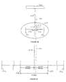
- Figure 5B shows in more detail the centerline 510 of the electron beam emerging from subfield 302 and the desired path 511 to the electronic optical axis 130 .
- the lines 524 & 526 denote the field of view within which it is desired that the centerline 510 of the electron beam be deflected by the pertinent first source 503 ( Figure 5A ).
- the lines 528 & 530 denote the field of view within which it is desired that the centerline 510 of the electron beam be deflected by the pertinent first source 503 in order for the error DAC 504 to correct the misalignment with the desired accuracy.
- the desired accuracy of a DAC to control the deflection of the electron beams from 20 subfields having a width of 1 millimeter and a grillage of 0.3 millimeters is calculated to be 23 bits.
- 23 bit DACs having the required speed are not presently commercially available. Therefore, it is desirable to provide the desired accuracy using DACs that are commercially available. For example, it would be desirable to achieve the desired accuracy using a 16 bit error DAC, which are commercially available at a reasonable cost and which have the required speed.
- the portion of the system within the ellipse 532 is shown enlarged in Figure 5C .
- the field of view is around the electronic optical axis 130 of the electronic lens system 104 .
- the first error DAC 504 could have an accuracy from 8 bits to 18 bits with the required accuracy of the first sources 503 adjusted to compensate for the selected accuracy of the first error DAC 504 .
- the 12 bit error DAC requires that the first sources 503 and the second sources 507 be much more accurate in deflecting the centerlines of the electron beams.
- FIG. 5D there is illustrated the device 500 as described above in conjunction with Figure 5A configured to correct the misalignment of the electronic optical axis 130 with the centerlines of the electron beams as the electronic optical axis 130 is moved to coincide with the centerlines of the electron beams emerging from each subfield.
- the functions of the elements of the device 500 shown and described in Figure 5D are the same as those shown and described in Figure 5A .
- the device 500 functions in Figure 5D to deflect or move the optical axis 130 to coincide with the centerlines of the electron beams emerging from the subfields in the reticle 102 .
- FIG. 5E & 5F there is shown in more detail the electronic optical axis 130 and the centerline 510 of an electron beam emerging from the subfield 302 .
- the lines 524 & 526 denote the boundaries of the electron beam emerging from the subfield 302 .
- the lines 528 & 530 denote the field of view within which it is desired that the electronic optical axis 130 be deflected by the pertinent first source 503 in order for the error DAC 504 to correct the misalignment with the desired accuracy.
- the desired accuracy of a DAC to control the deflection of the electronic optical axis 130 to be coincident with electron beams emerging from 20 subfields having a width of 1 millimeter and a grillage of 0.3 millimeters is calculated to be 23 bits.
- 23 bit DACs having the required speed are not commercially available. Therefore, it is desirable to provide the desired accuracy using DACs that are commercially available.
- the portion of the system within the ellipse 532 is shown enlarged in Figure 5F .
- the error DAC 508 ( Figure 5D ) has a 16 bit accuracy
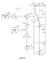
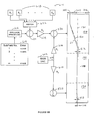
- the device 600 includes the electronic lens system 104 , a main DAC 602 having an output 604 that is amplified by an amplifier 606 having a gain G 1 and input via summer 520 to the deflection system in section 128 of the electronic lens system 104 .
- the deflection system in section 128 could be a magnetic deflection system or an electrostatic deflection system.
- the main DAC 602 has m discrete outputs corresponding to the number m of subfields in a row. As described above, the subfields in the reticle 102 may be separated by grillage. To account for the grillage when the electron beam is moved from subfield to subfield in a row, the output of a grillage DAC 608 after being reduced by a factor equal to the grillage G 3 , in this case 0.3 (0.3mm/mm), by amplifier 612 is summed by summer 520 with the output of amplifier 606 and input to the deflection system in section 128 .
- the output 604 from main DAC 602 is amplified by amplifier 610 having a gain G 2 and input via summer 522 to the deflection system in section 134 of the electronic lens system 104 . It is noted that there is only shown one input to summer 522 . The summer may have other inputs to affect the deflection system in section 134 . These other inputs are not an issue in the present invention and therefore are not shown or discussed.
- the device 614 includes the electronic lens system 104 , a control section comprising the main DAC 602 having an output 604 that is amplified by amplifier 606 having a gain G 1 and input to summer 520 .
- the output 604 is amplified by amplifier 610 having a gain G 2 and is input to summer 522 .
- the output of summer 522 is input to the third section 134 of the electronic lens system 104 .
- the grillage DAC because of the grillage between the columns, it is necessary to account for the grillage when moving from one subfield to the next in a row. Because the device 614 is insensitive to position errors caused by the main DAC 602 as described above, it is necessary for the grillage DAC to have the necessary accuracy in order to not degrade the position accuracy.
- the desired accuracy can be obtained with a 16 bit DAC rather than a 21 bit DAC by using a 16 bit DAC as a grillage error DAC 616 having m error inputs from an error table 619 , a switch 622 having m source inputs, S 1 to S m , 618 having high stability corresponding to the m subfields in a row on the reticle 102 .
- the grillage error DAC 616 has an output to a summer 620 that also has input from switch 622 .
- the error table 619 is constructed by running a calibration wafer through the system and tabulating the required corrections that are input to the grillage error DAC 616 .
- the output of summer 620 is amplified by amplifier 624 and input to summer 520 .
- the output of summer 520 is input to the deflection system in the first section 128 to control the deflection of the electron beams emerging from the subfields on the reticle 102 .
- FIG. 6C there is shown the device 600 and method shown in Figure 6A configured to correct the misalignment of the electronic optical axis 130 with the centerlines of the electron beams emerging from the subfields in the reticle 102 as the electronic optical axis 130 is moved to coincide with the centerlines, such as the centerline 510 .
- the grillage DAC 608 in order to obtain the necessary accuracy, must have an accuracy of 21 bits. And as discussed above, 21 bit DACs having the required speed are not commercially available.
- FIG. 6D there is illustrated the device 614 as shown in Figure 6B configured to correct the misalignment of the electronic optical axis 130 with the centerlines of the electron beams emerging from the subfields in the reticle 102 as the electronic optical axis 130 is moved to coincide with the centerlines, such as the centerline 510 emerging from subfield 302 .
- the inputs to summers 520 & 522 are the same as described above in the discussion of Figure 6B and the outputs of summers 520 & 522 control the deflection systems in the first and third sections of the lens system 104 , respectively.
- the deflection system in the first section 128 of the lens system 104 moves the electronic optical axis 130 to coincide with the electron beams emerging from the subfields in the reticle 102 and the deflection system in the third section 134 moves the electronic optical axis 130 to coincide with the centerlines of the electron beams.
- the device 700 includes a ramp generator 702 having an output 706 that is amplified by the amplifier 606 having a gain G 1 and input via summer 520 to the deflection system in section 128 of the electronic lens system 104 .
- the areas on the reticle in this case are not separated by grillage in the direction of electronic scanning and the ramp generator 702 moves the electron beam from area to area on the reticle rather than the electron beam being stepped from subfield to subfield.
- FIG. 7B there is illustrated the device 700 as shown in Figure 7A configured to correct the misalignment of the electronic optical axis 130 with the centerlines of the electron beam emerging from the reticle 102 as the electronic optical axis 130 is moved to coincide with the centerlines, such as the centerline 511 emerging from the reticle 102 .
- the inputs to summers 520 & 522 are the same as described above in the discussion of Figure 7A and the outputs of summers 520 & 522 control the deflections systems in the first and third sections of the lens system 104 , respectively.
- the deflection system in the first section 128 of the lens system 104 moves the electronic optical axis 130 to coincide with the electron beam emerging from the reticle 102 and the deflection system in the third section 134 moves the electronic optical axis 130 to coincide with the centerlines of the electron beam.
- FIG. 8 there is shown an electron beam 800 being deflected from the reticle 802 to the wafer 804 through the electronic lens system 104 .
- the electron beam 800 is shown being deflected without deflection error through the electronic lens system 104 .
- FIG 9 there is shown the electron beam 800 as shown in Figure 8 being deflected from the reticle 802 to the wafer 804 .
- the electron beam 800 is shown being deflected with a deflection error ⁇ R .
- the electron beam 800 deflected without a deflection error is reproduced in dashed outline and the parameters are shown unprimed.
- the parameters of the electron beam 800 that is deflected with deflection error ⁇ R are shown primed.
- the results and advantages of the electron-beam lithography systems of the present invention can now be more fully realized.
- the desired accuracy at the wafer can be obtained by utilizing commercially available 16 bit DACs.
- the electronic lens system in the electron-beam lithography system is made insensitive to position errors in the deflection control systems.
Landscapes
- Chemical & Material Sciences (AREA)
- Engineering & Computer Science (AREA)
- Nanotechnology (AREA)
- Analytical Chemistry (AREA)
- Physics & Mathematics (AREA)
- Mathematical Physics (AREA)
- Theoretical Computer Science (AREA)
- Crystallography & Structural Chemistry (AREA)
- Electron Beam Exposure (AREA)
- Exposure And Positioning Against Photoresist Photosensitive Materials (AREA)
Applications Claiming Priority (2)
| Application Number | Priority Date | Filing Date | Title |
|---|---|---|---|
| US177675 | 1980-08-13 | ||
| US09/177,675 US6133987A (en) | 1998-10-22 | 1998-10-22 | Technique for reducing pattern placement error in projection electron-beam lithography |
Publications (2)
| Publication Number | Publication Date |
|---|---|
| EP0996143A2 true EP0996143A2 (fr) | 2000-04-26 |
| EP0996143A3 EP0996143A3 (fr) | 2006-11-15 |
Family
ID=22649533
Family Applications (1)
| Application Number | Title | Priority Date | Filing Date |
|---|---|---|---|
| EP99121177A Withdrawn EP0996143A3 (fr) | 1998-10-22 | 1999-10-22 | Procédé de réduction des erreurs de positionnement des motifs en lithographie par faisceau électronique par projection |
Country Status (3)
| Country | Link |
|---|---|
| US (1) | US6133987A (fr) |
| EP (1) | EP0996143A3 (fr) |
| JP (1) | JP2000138166A (fr) |
Families Citing this family (2)
| Publication number | Priority date | Publication date | Assignee | Title |
|---|---|---|---|---|
| US6521903B1 (en) * | 1999-07-07 | 2003-02-18 | Nikon Corporation | Deflection noise reduction in charged particle beam lithography |
| US8299446B2 (en) * | 2009-08-12 | 2012-10-30 | Ultratech, Inc. | Sub-field enhanced global alignment |
Family Cites Families (11)
| Publication number | Priority date | Publication date | Assignee | Title |
|---|---|---|---|---|
| US4410879A (en) * | 1980-10-31 | 1983-10-18 | Tektronix, Inc. | High resolution digital-to-analog converter |
| US4430642A (en) * | 1981-10-02 | 1984-02-07 | Westinghouse Electric Corp. | Digital-to-analog converter |
| JPS5956727A (ja) * | 1982-09-27 | 1984-04-02 | Fujitsu Ltd | 電子ビ−ム露光装置 |
| US4998108A (en) * | 1990-07-30 | 1991-03-05 | International Business Machines Corporation | Large range, high speed, high accuracy digital-to-analog converter |
| US5153592A (en) * | 1991-04-30 | 1992-10-06 | Texas Instruments Incorporated | 16 bit error-correcting digital-to-analog converter |
| US5345085A (en) * | 1993-03-26 | 1994-09-06 | Etec Systems, Inc. | Method and structure for electronically measuring beam parameters |
| US5530250A (en) * | 1993-10-20 | 1996-06-25 | Nec Corporation | Electron beam deflecting apparatus with reduced settling time period |
| US5546319A (en) * | 1994-01-28 | 1996-08-13 | Fujitsu Limited | Method of and system for charged particle beam exposure |
| US5757010A (en) * | 1996-12-18 | 1998-05-26 | International Business Machines Corporation | Curvilinear variable axis lens correction with centered dipoles |
| JPH10256136A (ja) * | 1997-03-14 | 1998-09-25 | Nikon Corp | 荷電ビーム露光装置 |
| JPH10275581A (ja) * | 1997-03-28 | 1998-10-13 | Nikon Corp | 荷電粒子光学系 |
-
1998
- 1998-10-22 US US09/177,675 patent/US6133987A/en not_active Expired - Fee Related
-
1999
- 1999-10-18 JP JP11294981A patent/JP2000138166A/ja active Pending
- 1999-10-22 EP EP99121177A patent/EP0996143A3/fr not_active Withdrawn
Also Published As
| Publication number | Publication date |
|---|---|
| EP0996143A3 (fr) | 2006-11-15 |
| US6133987A (en) | 2000-10-17 |
| JP2000138166A (ja) | 2000-05-16 |
Similar Documents
| Publication | Publication Date | Title |
|---|---|---|
| KR100998770B1 (ko) | 하전 입자 빔 묘화 장치, 패턴의 치수 오차 보정 장치 및 패턴의 치수 오차 보정 방법 | |
| US10453652B2 (en) | Multi charged particle beam writing apparatus and multi charged particle beam writing method | |
| US20030107006A1 (en) | Charged particle beam exposure method and apparatus | |
| KR20200005443A (ko) | 멀티 전자 빔 조사 장치, 멀티 전자 빔 조사 방법, 및 멀티 전자 빔 검사 장치 | |
| JP2004303794A (ja) | 露光装置 | |
| JP7180515B2 (ja) | マルチ荷電粒子ビーム描画装置及びマルチ荷電粒子ビーム描画方法 | |
| US10607812B2 (en) | Multiple charged particle beam writing apparatus, and multiple charged particle beam writing method | |
| US20190035603A1 (en) | Multi charged particle beam writing apparatus and multi charged particle beam writing method | |
| EP0367126B1 (fr) | Méthode d'exposition au rayonnement de particules chargées utilisant un masque | |
| US12609278B2 (en) | Multi charged particle beam writing method and multi charged particle beam writing apparatus | |
| KR100327009B1 (ko) | 전자빔 노출 방법 및 전자빔 노출 장치 | |
| US4692579A (en) | Electron beam lithography apparatus | |
| EP0148784B1 (fr) | Etalonnage d'appareil à faisceau d'électrons | |
| US6133987A (en) | Technique for reducing pattern placement error in projection electron-beam lithography | |
| KR20000076936A (ko) | 전자 빔 리소그라피 방법 및 그 제조장치 | |
| JP4183454B2 (ja) | 電子ビーム描画装置 | |
| US20020070356A1 (en) | Electron beam proximity exposure apparatus and mask unit therefor | |
| US6277531B1 (en) | Charged-particle-beam microlithography apparatus and methods including focal-point correction | |
| US6376137B1 (en) | Charged-particle-beam microlithography apparatus and methods including correction of stage-positioning errors using a deflector | |
| US20250299918A1 (en) | Position measurement apparatus, charged particle beam writing apparatus, and mark position measurement method | |
| US20240429022A1 (en) | Multiple charged particle beam writing apparatus and multiple charged particle beam writing method | |
| US20250364208A1 (en) | Background waveform acquisition method, mark position detection method, electron beam writing method, and electron beam writing apparatus | |
| US20250372346A1 (en) | Mark position measurement method, multi-charged particle beam writing method and multi-charged particle beam writing apparatus | |
| US20250087452A1 (en) | Multiple charged particle beam writing apparatus and multiple charged particle beam writing method | |
| JP2025082378A (ja) | マーク位置計測装置及びマーク位置計測方法 |
Legal Events
| Date | Code | Title | Description |
|---|---|---|---|
| PUAI | Public reference made under article 153(3) epc to a published international application that has entered the european phase |
Free format text: ORIGINAL CODE: 0009012 |
|
| AK | Designated contracting states |
Kind code of ref document: A2 Designated state(s): AT BE CH CY DE DK ES FI FR GB GR IE IT LI LU MC NL PT SE |
|
| AX | Request for extension of the european patent |
Free format text: AL;LT;LV;MK;RO;SI |
|
| RIC1 | Information provided on ipc code assigned before grant |
Ipc: H01J 37/153 20060101ALN20060712BHEP Ipc: H01J 37/147 20060101ALI20060712BHEP Ipc: H01J 37/317 20060101AFI20000204BHEP |
|
| PUAL | Search report despatched |
Free format text: ORIGINAL CODE: 0009013 |
|
| AK | Designated contracting states |
Kind code of ref document: A3 Designated state(s): AT BE CH CY DE DK ES FI FR GB GR IE IT LI LU MC NL PT SE |
|
| AX | Request for extension of the european patent |
Extension state: AL LT LV MK RO SI |
|
| AKX | Designation fees paid | ||
| STAA | Information on the status of an ep patent application or granted ep patent |
Free format text: STATUS: THE APPLICATION IS DEEMED TO BE WITHDRAWN |
|
| 18D | Application deemed to be withdrawn |
Effective date: 20061102 |
|
| REG | Reference to a national code |
Ref country code: DE Ref legal event code: 8566 |