EP0996169A2 - Halbleiteranordnung mit einer Begrenzungsschicht - Google Patents
Halbleiteranordnung mit einer Begrenzungsschicht Download PDFInfo
- Publication number
- EP0996169A2 EP0996169A2 EP99120752A EP99120752A EP0996169A2 EP 0996169 A2 EP0996169 A2 EP 0996169A2 EP 99120752 A EP99120752 A EP 99120752A EP 99120752 A EP99120752 A EP 99120752A EP 0996169 A2 EP0996169 A2 EP 0996169A2
- Authority
- EP
- European Patent Office
- Prior art keywords
- layer
- period
- carrier confinement
- semiconductor device
- electrons
- Prior art date
- Legal status (The legal status is an assumption and is not a legal conclusion. Google has not performed a legal analysis and makes no representation as to the accuracy of the status listed.)
- Withdrawn
Links
- 239000004065 semiconductor Substances 0.000 title claims abstract description 51
- 239000000969 carrier Substances 0.000 claims description 17
- 239000000758 substrate Substances 0.000 description 16
- 229910001218 Gallium arsenide Inorganic materials 0.000 description 13
- 239000010931 gold Substances 0.000 description 12
- JBRZTFJDHDCESZ-UHFFFAOYSA-N AsGa Chemical compound [As]#[Ga] JBRZTFJDHDCESZ-UHFFFAOYSA-N 0.000 description 11
- 238000005381 potential energy Methods 0.000 description 10
- 238000010586 diagram Methods 0.000 description 8
- 238000002310 reflectometry Methods 0.000 description 8
- 230000003247 decreasing effect Effects 0.000 description 7
- 239000012535 impurity Substances 0.000 description 7
- PCHJSUWPFVWCPO-UHFFFAOYSA-N gold Chemical compound [Au] PCHJSUWPFVWCPO-UHFFFAOYSA-N 0.000 description 6
- 229910052737 gold Inorganic materials 0.000 description 6
- 238000006243 chemical reaction Methods 0.000 description 5
- 150000001875 compounds Chemical class 0.000 description 5
- 229910052732 germanium Inorganic materials 0.000 description 5
- 239000000463 material Substances 0.000 description 5
- 238000005229 chemical vapour deposition Methods 0.000 description 4
- 238000000151 deposition Methods 0.000 description 4
- 230000008021 deposition Effects 0.000 description 4
- 230000000694 effects Effects 0.000 description 4
- GNPVGFCGXDBREM-UHFFFAOYSA-N germanium atom Chemical compound [Ge] GNPVGFCGXDBREM-UHFFFAOYSA-N 0.000 description 4
- 229910052751 metal Inorganic materials 0.000 description 4
- 239000002184 metal Substances 0.000 description 4
- 238000000034 method Methods 0.000 description 4
- 239000011701 zinc Substances 0.000 description 4
- 230000005684 electric field Effects 0.000 description 3
- 239000000203 mixture Substances 0.000 description 3
- 230000008569 process Effects 0.000 description 3
- 230000000644 propagated effect Effects 0.000 description 3
- 230000004044 response Effects 0.000 description 3
- 230000035945 sensitivity Effects 0.000 description 3
- HCHKCACWOHOZIP-UHFFFAOYSA-N Zinc Chemical compound [Zn] HCHKCACWOHOZIP-UHFFFAOYSA-N 0.000 description 2
- 230000008859 change Effects 0.000 description 2
- 230000007423 decrease Effects 0.000 description 2
- 230000006872 improvement Effects 0.000 description 2
- 238000009413 insulation Methods 0.000 description 2
- 230000004048 modification Effects 0.000 description 2
- 238000012986 modification Methods 0.000 description 2
- 238000000926 separation method Methods 0.000 description 2
- 239000007787 solid Substances 0.000 description 2
- 229910052725 zinc Inorganic materials 0.000 description 2
- GYHNNYVSQQEPJS-UHFFFAOYSA-N Gallium Chemical compound [Ga] GYHNNYVSQQEPJS-UHFFFAOYSA-N 0.000 description 1
- OAICVXFJPJFONN-UHFFFAOYSA-N Phosphorus Chemical compound [P] OAICVXFJPJFONN-UHFFFAOYSA-N 0.000 description 1
- 230000001133 acceleration Effects 0.000 description 1
- 238000009825 accumulation Methods 0.000 description 1
- 229910052782 aluminium Inorganic materials 0.000 description 1
- XAGFODPZIPBFFR-UHFFFAOYSA-N aluminium Chemical compound [Al] XAGFODPZIPBFFR-UHFFFAOYSA-N 0.000 description 1
- RBFQJDQYXXHULB-UHFFFAOYSA-N arsane Chemical compound [AsH3] RBFQJDQYXXHULB-UHFFFAOYSA-N 0.000 description 1
- 229910052785 arsenic Inorganic materials 0.000 description 1
- RQNWIZPPADIBDY-UHFFFAOYSA-N arsenic atom Chemical compound [As] RQNWIZPPADIBDY-UHFFFAOYSA-N 0.000 description 1
- 229910000070 arsenic hydride Inorganic materials 0.000 description 1
- 230000004888 barrier function Effects 0.000 description 1
- 230000008901 benefit Effects 0.000 description 1
- 239000002772 conduction electron Substances 0.000 description 1
- 239000013078 crystal Substances 0.000 description 1
- 238000000354 decomposition reaction Methods 0.000 description 1
- 238000009792 diffusion process Methods 0.000 description 1
- 230000005284 excitation Effects 0.000 description 1
- 229910052733 gallium Inorganic materials 0.000 description 1
- 229910021478 group 5 element Inorganic materials 0.000 description 1
- 229910052738 indium Inorganic materials 0.000 description 1
- APFVFJFRJDLVQX-UHFFFAOYSA-N indium atom Chemical compound [In] APFVFJFRJDLVQX-UHFFFAOYSA-N 0.000 description 1
- 150000002500 ions Chemical class 0.000 description 1
- 230000001678 irradiating effect Effects 0.000 description 1
- 238000010030 laminating Methods 0.000 description 1
- 230000007246 mechanism Effects 0.000 description 1
- 229910052698 phosphorus Inorganic materials 0.000 description 1
- 239000011574 phosphorus Substances 0.000 description 1
- 230000001902 propagating effect Effects 0.000 description 1
- 229910052594 sapphire Inorganic materials 0.000 description 1
- 239000010980 sapphire Substances 0.000 description 1
- 230000005641 tunneling Effects 0.000 description 1
Images












Classifications
-
- B—PERFORMING OPERATIONS; TRANSPORTING
- B82—NANOTECHNOLOGY
- B82Y—SPECIFIC USES OR APPLICATIONS OF NANOSTRUCTURES; MEASUREMENT OR ANALYSIS OF NANOSTRUCTURES; MANUFACTURE OR TREATMENT OF NANOSTRUCTURES
- B82Y20/00—Nanooptics, e.g. quantum optics or photonic crystals
-
- H—ELECTRICITY
- H10—SEMICONDUCTOR DEVICES; ELECTRIC SOLID-STATE DEVICES NOT OTHERWISE PROVIDED FOR
- H10F—INORGANIC SEMICONDUCTOR DEVICES SENSITIVE TO INFRARED RADIATION, LIGHT, ELECTROMAGNETIC RADIATION OF SHORTER WAVELENGTH OR CORPUSCULAR RADIATION
- H10F77/00—Constructional details of devices covered by this subclass
- H10F77/10—Semiconductor bodies
- H10F77/14—Shape of semiconductor bodies; Shapes, relative sizes or dispositions of semiconductor regions within semiconductor bodies
- H10F77/146—Superlattices; Multiple quantum well structures
-
- H—ELECTRICITY
- H10—SEMICONDUCTOR DEVICES; ELECTRIC SOLID-STATE DEVICES NOT OTHERWISE PROVIDED FOR
- H10F—INORGANIC SEMICONDUCTOR DEVICES SENSITIVE TO INFRARED RADIATION, LIGHT, ELECTROMAGNETIC RADIATION OF SHORTER WAVELENGTH OR CORPUSCULAR RADIATION
- H10F77/00—Constructional details of devices covered by this subclass
- H10F77/10—Semiconductor bodies
- H10F77/14—Shape of semiconductor bodies; Shapes, relative sizes or dispositions of semiconductor regions within semiconductor bodies
- H10F77/146—Superlattices; Multiple quantum well structures
- H10F77/1465—Superlattices; Multiple quantum well structures including only Group IV materials, e.g. Si-SiGe superlattices
Definitions
- the present invention relates to a semiconductor device having a new structure.
- the new structure of the present invention is effective to an opto-electric conversion device, or a light-receiving device, or other pin diode, a variable capacity device having an nin, pip, pn - n, pp - n or pin junction structure.
- Pin diodes having the same characteristic of rectification as that of pn diodes are known. Also known are avalanche diodes, and Impact Avalanche Transit Time (IMPATT) diodes used by applying a backward voltage.
- IMPATT Impact Avalanche Transit Time
- a light-receiving device has been known to have a pin junction structure.
- a backward voltage is applied to the pin layers of the device, and electron-hole pairs are generated by that light incided from the side of a p-layer is absorbed in an i-layer.
- the electron-hole pairs excited in the i-layer are accelerated by a backward voltage in the i-layer, and electrons and holes are flowing into an n-layer and a p-layer, respectively.
- a photocurrent whose intensity varies according to an intensity of the incident light is outputted.
- a voltage-variable capacity device has been known to have a pn junction structure, whose p-layer having a high impurity concentration and n-layer having a low impurity concentration are jointed and form a depletion layer at a boundary region between the p-layer and the n-layer as a capacity device.
- a reverse bias voltage is applied to the pn junction of the variable capacity device, a width of the depletion layer is extended and a capacity of the variable capacity device is reduced.
- the capacity of the device varies according to a value of applied reverse bias voltage.
- the I-V characteristics of these diodes have a problem in that they are difficult to change because they are determined by the semiconductor materials constituting the diodes. Therefore, further improvement is required.
- the i-layer which absorbs light is formed to have a comparatively larger thickness. But when the thickness of the i-layer becomes thicker, more times are needed to draw carriers to the n-layer and the p-layer. As a result, the response velocity of the opto-electric conversion is lowered. To improve the velocity, an electric field in the i-layer is increased by increasing a backward voltage. But when the backward voltage is enlarged, an element separation become difficult and a leakage current is occurred. As a result, an photocurrent which flows when the device is not incided by light, or a dark current, is increased.
- the voltage-variable capacity device With respect to the voltage-variable capacity device, it is required to enlarge a variation rate of a capacity value toward an applied voltage. To enlarge the variation rate, forming space distribution in an impurity concentration has been suggested. And to enlarge the voltage variation rate, i.e., voltage-sensitivity, the impurity concentration is required to have a non-linear distribution with respect to a depth.
- An object of the present invention is to change the I-V characteristics when the backward voltage is applied to the pin diode.
- Another object of the present invention is to improve the light-receiving sensitivity and the response velocity of the opto-electric conversion by providing a light-receiving device having a pin junction of a completely new structure.
- an object of the present invention to provide a voltage-variable capacity device with high voltage-variation rate, i.e., high voltage sensitivity. Another object of the present invention is to improve a precision of a capacity controlled by an external voltage. The other object of the present invention is to expand a dynamic range of an applied voltage.
- a first aspect of the present invention is a semiconductor device constituted by a multi-period layer units and a carrier confinement layer therebetween.
- the multi-period layer unit has plural periods of a pair of a first layer and a second layer as a unit.
- the second layer has a wider band gap than the first layer.
- a carrier confinement layer is formed between the adjacent two of the multi-period layer units.
- a band gap of the carrier confinement layer is wider than that of the first layer.
- the second aspect of the present invention is to make the semiconductor device of the first aspect to be a pin-type diode, having a carrier confinement layer and a multi-period layer unit in an i-layer.
- the third aspect of the present invention is to form a light-receiving part in a p-layer or an n-layer of the pin diode of the second aspect.
- the light-receiving part generates carriers which is injected to the i-layer.
- the fourth aspect of the present invention is a semiconductor device constituted by a multi-period layer unit having plural periods of a pair of a first layer and a second layer as a unit.
- the second layer has a wider band gap than the first layer.
- a carrier confinement layer is formed between the adjacent two multi-period layer units.
- a band gap of the carrier confinement layer is narrower than that of the second layer.
- the fifth aspect of the present invention is to make the semiconductor device of the fourth aspect to be a light-receiving device having a pin junction structure. And a carrier confinement layer and a multi-period layer unit are formed in an i-layer.
- the sixth aspect of the present invention is to make the semiconductor device of the fourth aspect to be a light-receiving device having a carrier confinement layer and a multi-period layer unit that are formed in an n-layer or a p-layer.
- the seventh aspect of the present invention is to make a semiconductor device of the sixth aspect to be a device having a pn junction structure.
- the eighth aspect of the present invention is to form a carrier confinement layer, having the same band width as that of the first layer, in the semiconductor device of one of the first, fourth and sixth aspect of the present invention.
- the ninth aspect of the present invention is to make the semiconductor device of the first aspect to be a variable capacity device having an nin or pip junction structure.
- a carrier confinement layer and a multi-period layer unit are formed in an i-layer of the variable capacity device.
- the tenth aspect of the present invention is to make the semiconductor device of the first aspect to be a variable capacity device having a pn - n, pp - n or pin junction structure.
- a carrier confinement layer and a multi-period layer unit are formed in an n - layer, p - -layer or an i-layer.
- the eleventh aspect of the present invention is to form a carrier confinement layer, having the same band width as that of the second layer, in the semiconductor device of the first or the third aspect, and the ninth or the tenth aspects of the present invention.
- FIG. 1A shows a conduction band of a multi-period layer formed in an i-layer. Electrons, or minority carriers, are injected into the i-layer, or conduct from left to right as shown by an arrow in FIGS. 1A and 1B. Among the electrons, those that exist near the bottom of the conduction band of the second layer B are likely to contribute to conduction. The electrons near the bottom of the conduction band of the second layer B have a kinetic energy E. Accordingly, the electrons in the first layer W have a kinetic energy E+V and are thus accelerated by the potential energy V due to the band gap difference between the first layer W and the second layer B.
- L 1 and L 2 ; m 1 * and m 2 *; and E 1 and E 2 represents thicknesses of the first layer W and the second layer B; effective mass of electrons; and an energy of electrons, respectively.
- h, and m and n represents Plank's constant, and odd numbers, respectively.
- each thickness of the first and the second layers is determined by multiplying by odd number one fourth of quantum-wave wavelength in each of the first and the second layers.
- Takagi shows multi-quantum barriers each having a band gap energy represented by E 1 and E 2 equal to 2V, respectively
- the inventor of the present invention suggests a multi-period layer which functions as a reflecting layer with much smaller energy than V.
- E 1 and E 2 in Eqs. 1 and 2 is prefer to be defined as the kinetic energy of the electrons at the level near the lowest energy level of the conduction band of the second layer B.
- the present invention is not necessary to be limited to the multi-period layer satisfied with the disclosed condition above.
- the energy level of the multi-period layer band inclines by the external voltage as shown in FIG. 1B.
- E+V and E or kinetic energy of the electrons in the first layer W and the second layer B respectively, increase according to a propagating of quantum-wave. Accordingly, the thicknesses of the first layer W and the second layer B no longer improve the quantum-wave reflectivity of the electrons injected into the i-layer.
- the thicknesses of the first layer W and the second layer B are determined for selectively reflecting either the holes or the electrons, because of the difference in potential energy between the valence and the conduction bands, and the difference in effective mass of holes and electrons in the first layer W and the second layer B.
- the optimum thickness for reflecting electrons is not the optimum thickness reflecting holes.
- the thickness for selectively reflecting electrons is designed based on the difference in the potential energy of the conduction band and on the effective mass of electrons.
- the thickness for selectively reflecting holes is designed based on the difference in the potential energy of the valence band and on the effective mass of holes, forming another type of multi-period layer in an n-layer for reflecting only holes and allowing electrons to pass through.
- Forming the multi-period layers of electrons in a p-layer as described above enable I-V characteristic of the diode to vary rapidly and the dynamic resistance of the diode to be lowered sharply.
- Multi-period layer units having a plurality of multi-layer structures are connected in series and at certain intervals, and a carrier confinement layer, which has a wider band gap than the first layer W, is formed between the respective multi-period layer units. Then I-V characteristic of each multi-period layer units varies in accordance with the quantity of carriers accumulated in the carrier confinement layer. That is, the diode of the present invention can be used as a semiconductor diode, i.e., a photodiode, which detects a generation of carriers by an external factor.
- I-V characteristic of the diode can be varied in a step at various points.
- the diode of the present invention can be used as a photodiode such as a light detector.
- FIG. 2 shows an energy diagram of a conduction band and a valence band when an external voltage is applied to the interval between the p-layer and the n-layer in a forward direction.
- the conduction band of the i-layer becomes plane by applying the external voltage.
- Four multi-period layer units Q 1 to Q 4 are formed in the i-layer, and carrier confinement layers C 1 to C 3 , having a narrower band gap than the second layer, are formed at each intervals of the multi-period layer units.
- a conduction band of a multi-period layer unit Q 1 is as shown in FIG. 1A.
- kinetic energy of electrons in the conduction band is modulated by potential energy due to the multi-layer structure.
- the multi-period layer When thicknesses of the first layer W and the second layer B are equal to order of quantum-wave wavelength, electrons tend to have characteristics of a wave.
- the multi-period layer When the multi-period layer is formed by the first layer W and the second layer B, whose thicknesses are determined so as to satisfy equations 1 and 2, the multi-period layer functions as an electron reflecting layer.
- the holes existing in the valence band of the multi-period layer unit behave as explained in the first to third aspects of the present invention. Consequently, the multi-period layer having the structure described above can reflect only electrons and allowing holes to pass through. Further, thicknesses of the first layer W and the second layer B are designed based on the difference in the potential energy of the valence band and on the effective mass of holes, forming another type of multi-period layer in an n-layer for reflecting only holes and allowing electrons to pass through. Accordingly, the multi-period layer unit which reflects holes and functions as a hole reflecting layer can be formed to connect in series to each of the multi-period layer units described above, which reflects only holes.
- the light-receiving device described above having a multi-period layer unit can have a state not to occur electric current by reflecting carriers selectively in a range of 0 V to a certain value of a bias voltage. Accordingly, the light-receiving device can be formed by only one of the n-layer and the p-layer in which the multi-period layer units and the carrier confinement layer are formed. Alternatively, the light-receiving device can be formed by a pn junction structure with a p-layer and an n-layer, in at least one of which the multi-period layer units and the carrier confinement layer are formed.
- the eighth aspect of the present invention is to form the band width of the carrier confinement layer to have the same band width as that of the first layer W.
- Each pairs of electron and hole generated by irradiating light are easily accumulated in a conduction band and a valence band of the carrier confinement layer.
- the carrier confinement layer has the same band width as that of the first layer W, carriers existing in the carrier confinement layer behave as those existing in the multi-period layer unit. Consequently, an ability of the light-receiving device is improved.
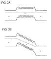
- a carrier confinement layer or a multi-period layer of the present invention is explained hereinafter, referring to an nin structure shown in FIGS. 3A and 3B as an example.
- kinetic energy of electrons in the conduction band is modulated by potential energy due to the multi-layer structure.
- thicknesses of the first layer W and the second layer B are equal to order of quantum-wave wavelength, electrons tend to have characteristics of a wave.
- the multi-period layer is formed by the first layer W and the second layer B, whose thicknesses are determined so as to satisfy equations 1 and 2, the multi-period layer functions as an electron reflecting layer.
- FIGS. 1B and 3B show an energy level gradient occurring in the multi-period layer on the condition that the external voltage is applied to the i-layer. Then E+V and E, kinetic energies of the first layer W and the second layer B, respectively, are enlarged according to propagation of the quantum-wave, and each thickness of the first layer W and the second layer B become apart from the most suitable condition to have an effective reflectivity.
- the thickness of the first layer W and the second layer B are determined for selectively reflecting the holes or the electrons, because of the difference in potential energy between the valence and the conduction bands, and the difference in effective mass of holes and electrons in the first layer W and the second layer B.
- the optimum thickness for reflecting electrons is not the optimum thickness for reflecting holes. Accordingly, holes do not exist in the i-layer when the applied voltage is small, and the i-layer is completely depleted with respect to holes.
- Plurality of multi-period layer units and a carrier confinement layer formed between each of the multi-period layer units are cascaded, i.e., connected in series, and a capacity of the device is enlarged.
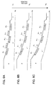
- FIGS. 4A to 4C show the structure of the multi-period layer.
- Each multi-period layer units A 1 to A 4 are formed at certain intervals, and each carrier confinement layers C 1 to C 3 are formed at the interval of each multi-period layer units A 1 to A 4 . Electrons existing in the i-layer are confined effectively by the carrier confinement layers C 1 to C 3 , and a capacity of the device is enlarged.
- an applied voltage is increased, a quantum-wave wavelength of electrons existing in each multi-period layer units A 1 to A 4 do not satisfy a condition to reflect electrons, which are accelerated to flow by an electric field of the i-layer. Accordingly, an electron concentration of each carrier confinement layers C 1 to C 3 is decreased, and the capacity of the i-layer becomes smaller. Thus controlling the capacity is possible by applying an external voltage.
- the nin-type can be an pip-type and carriers can be holes alternative to electrons.
- the eleventh aspect of the present invention is to form the band width of the carrier confinement layer to have the same band width as that of the second layer B. Because of that, carriers existing in the carrier confinement layer behave as those existing in the multi-period layer unit. Consequently, an ability of the variable capacity device is improved.
- FIG. 1A shows a conduction band of a multi-period layer having a multi-layer structure with plural periods of a first layer W and a second layer B as a unit formed in an n - -layer.
- the multi-period layer when the multi-period layer is formed by the first layer W and the second layer B, whose thicknesses are determined so as to satisfy equations 1 and 2, the multi-period layer functions as an electron reflecting layer.
- the holes existing in the valence band of the multi-period layer unit behave completely the same as those in the i-layer of the nin-type variable capacity device. Accordingly, holes do not exist in the n - -layer when the applied voltage is small, and the n - -layer is completely depleted with respect to holes.
- a plurality of multi-period layer units and a carrier confinement layer formed between each of the multi-period layer units, are cascaded, i.e., connected in series, and a capacity of the device is enlarged.
- the pn - n structure can be a pp - n or pin structure.
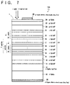
- FIG. 7 is a sectional view of a pin diode 100 in which a multi-period layer is formed in an i-layer.
- the pin diode 100 has a substrate 10 made of gallium arsenide (GaAs).
- GaAs buffer layer 12 of n-type conduction having a thickness generally of 0.3 ⁇ m and an electron concentration of 2 x 10 18 /cm 3 , is formed on the substrate 10.
- An n-Ga 0.51 In 0.49 P contact layer 14 of n-type conduction having a thickness generally of 0.13 ⁇ m and electron concentration of 2 x 10 18 /cm 3 , is formed on the buffer layer 12.
- n-Al 0.51 In 0.49 P n-layer 16 having a thickness generally of 0.2 ⁇ m and an electron concentration of 1 x 10 18 /cm 3 , is formed on the contact layer 14.
- a non-doped i-layer 18 is formed on the n-layer 16.
- An Al 0.51 In 0.49 P p-layer 20, having a thickness generally of 0.2 ⁇ m and a hole concentration of 1 x 10 18 /cm 3 is formed on the i-layer 18.
- a p-Ga 0.51 In 0.49 P contact layer 22 of p-type conduction having a thickness generally of 0.13 ⁇ m and a hole concentration of 2 x 10 18 /cm 3 , is formed on the p-layer 20.
- a p-GaAs first contact layer 24 of p-type conduction having a thickness generally of 0.06 ⁇ m and a hole concentration of 2 x 10 18 /cm 3 , is formed on the contact layer 22.
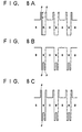
- FIGS. 8A to 8C show a structure of the multi-period layer unit A 1 in detail.
- the first layer W has a thickness of 5 nm
- the second layer B has a thickness of 7nm.
- a non-doped ⁇ layer made of Al 0.33 Ga 0.33 In 0.33 P is formed at each interface between the first layer W and the second layer B.
- a non-doped Al 0.51 In 0.49 P carrier confinement layer C having a thickness of 14 nm, is formed between any multi-period layer units A 1 and A i+1 , respectively, as shown in FIG. 9.
- the second layer B which contact to the p-layer 20 and the n-layer 16 have a thickness of 0.05 ⁇ m.
- the first second layer B was formed thicker than other second layers B in order to prevent conduction by tunneling effects from the n-layer 16 or the p-layer 20 into the first layer W.
- the substrate 10 has a diameter of 2.0 inches and the normal direction of its main surface is offset toward the [011] axis by 15 degree from the (100) plane.
- the pin diode 100 was manufactured by gas source molecular beam epitaxial deposition (GS-MBE), which is an epitaxial growth method performed under extremely a high vacuum condition.
- GS-MBE is different from a conventional MBE, which supplies group III and V elements both from the solid sources.
- group III elements such as indium (In), gallium (Ga), and aluminum (Al) are supplied from a solid source and group V elements such as arsenic (As) and phosphorus (P) are supplied by heat decomposition of gas material such as AsH 3 and PH 3 .
- the pin diode 100 can be manufactured by metal organic chemical vapor deposition (MOCVD).
- MOCVD metal organic chemical vapor deposition
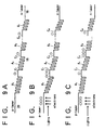
- Each multi-period layer units A 1 to A 7 reflects electrons, which are generated in the p-layer 20 as minority carriers, and electrons are not conducted in the i-layer 18.
- the ⁇ layer is not shown in FIGS. 9A and 9B, it is present at each interface between the first layer W and the second layer B, as shown in FIGS. 8A to 8C.
- FIG. 9A shows an electric potential gradient occurring in the i-layer 18 as an insulation layer on the condition that a backward voltage is applied to the interface between the p-layer 20 and the n-layer 16 of the diode 100.
- the multi-period layer unit A 1 Because of the backward voltage applied to the multi-period layer unit A 1 , its reflectivity of electrons is lowered and minority carriers generated in the p-layer 20 start to flow as a small quantity of leakage current. The minority carriers are conducted in the first multi-period layer unit A 1 , and flows into the first carrier confinement layer C 1 . This accumulation of electrons in the confinement layer C 1 makes an electric potential gradient of the multi-period layer unit A 1 steeper and the multi-period layer unit A 2 adjacent to A 1 gentler. Consequently, the kinetic energy of electrons injected into the multi-period layer unit A 1 becomes larger than that used to design each thicknesses of the respective layers of the multi-period layer unit A 1 .
- the reflectivity of the multi-period layer unit A 1 becomes smaller, and more electrons pass through the multi-period layer unit A 1 and are accumulated in the carrier confinement layer C 1 . Then, the electric potential gradient of the second multi-period layer unit A 2 becomes gentler, and its reflectivity improves. Electrons are thus accumulated in the carrier confinement layer C 1 effectively.
- the same process occurs between the second and the third multi-period layer units A 2 and A 3 , and electrons in the carrier confinement layer C 1 leak into an electron confinement layer C 2 by a small quantity.
- the electric potential gradient of the second multi-period layer unit A 2 becomes steeper, but, the electric potential gradients of the first and the third multi-period layer units A 1 and A 3 become gentler.
- the reflectivities of the first and the third multi-period layer unit improve.
- I-V characteristic was measured when the backward voltage is applied to the pin diode 100. As shown in FIG. 10, until a backward voltage is 27.6 V, the electric current is substantially small, about 10 -5 A. when the backward voltage is above 27.6 V, the electric current increases sharply, at certain plural voltage values.
- a window L is formed on the surface of the p-layer 24.
- the p-layers 20-24 corresponding the window L function as a light receiver which receives lights and generates electrons.
- I-V characteristic was measured when the backward voltage is applied to the pin diode 100 and the result is shown in FIG. 11.
- Electrons, light-excited in the p-layer 20, are propagated through the i-layer 18 by a mechanism described above, as shown in FIG. 11, an electric current occurs for a small quantity of a backward voltage because of the electrons generated by light excitation. Also, the electric current increases step by step, at certain plural backward voltages.
- the electric current when the diode is irradiated by light represented by A
- the electric current obtained when the diode is irradiated by light detector in this range, is substantially lower compared to that of an avalanche photo diode in the prior art.
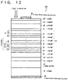
- FIG. 12 shows a sectional view of a light-receiving device 200 having the same structure as that of the pin diode 100 in Example 1, except for that of the following.
- Q 2 , ..., Q 4 are formed like Q 1 , and 4 multi-period layer units in total are formed in the i-layer 18.
- FIGS. 8A to 8C show a structure of the multi-period layer unit Q 1 in detail.
- Non-doped Ga 0.51 In 0.49 P carrier confinement layers C 1 to C 3 are formed between any multi-period layer units Q i and Q i+1 , respectively.
- the second layers B which contact to the n-layer 16 and the p-layer 20 have a thickness of 0.05 ⁇ m, respectively.
- the substrate 10 has a diameter of 2.0 inches and the normal direction of its main surface is offset toward the [011] axis by 15 degree from the (100) plane, just as same as the substrate 10 of Example 1.
- the light-receiving device 200 was manufactured by gas source molecular beam epitaxial deposition (GS-MBE) as in Example 1.
- the light-receiving device 200 can be manufactured by metal organic chemical vapor deposition (MOCVD).
- the light-receiving device 200 has a high opto-electric conversion effectivity because electrons, which are excited in the carrier confinement layers C 1 to C 3 , function as a gate-controlled switch toward the conduction of electrons from the n-layer 16 to the p-layer 20.
- a condition to reflect electrons is satisfied in the multi-period layer units Q 1 to Q 4 .
- electrons may be conducted in the multi-period layer units Q 1 to Q 4 as a wave. Accordingly, a switching velocity is considered to be larger.
- Measured I-V characteristic of the light-receiving device 200 is shown in FIG. 13.
- the photocurrent rises abruptly from 10 -11 to 10 -7 A, or in the range of 4 orders, at the forward voltage of 0.2 V.
- a forward voltage is applied to the device, a dark current is suppressed a lower value and degree of increasing is also suppressed.
- the phenomenon is occurred because the dark electrons reflected by the multi-period layer units and the dark current is kept comparatively lower.
- the photocurrent when the device is incided by light, represented by A1, is about hundredfold that of a dark current, represented by B1.
- the forward applied voltage at which an electric potential gradient in the i-layer 18 becomes plane is appeared to be 1 V.
- the photocurrent is not less than 5 x 10 -6 A.
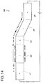
- a light-receiving device 300 having an nipin structure shown in FIG. 14 is formed.
- the regions represented by a1, a2, a3 are the same regions as those in the light-receiving device 200 having an nip structure.
- a multi-period layer and a carrier confinement layer are formed in an i-layer a2.
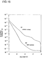
- Regions a4 and a5 function to draw the photocurrent which flows into the p-type region a3 by a reverse external bias voltage. I-V characteristic was measured when the light-receiving device 300 is incided by light.
- the photocurrent, represented by A2 is about thousandfold that of a dark current, represented by B2.
- a light-receiving device 400 using Si/Ge compound semiconductor shown in FIG. 16 is formed.
- a first layer W made of Si 0.8 Ge 0.2 and a second layer B made of Si are formed to have thicknesses of 5 nm and 7 nm, respectively.
- Carrier confinement layers C 1 to C 3 made of Si 0.8 Ge 0.2 is formed to have a thickness of 20 nm. No ⁇ layer is formed in the device 400.
- a characteristic of the device 400 was measured when the device is incided by light. As shown in FIG. 17, the photocurrent, represented by A3, is thousand fold that of a dark current, represented by B3. When the estimated forward voltage between n-layer a1 and p-layer a3 is about 0.9 V, the photocurrent rises abruptly. Further, by forming a ⁇ layer, the characteristic of the light-receiving device 400 will be improved.
- the light-receiving device of the present invention can obtain a larger S/N ratio compared with conventional devices.
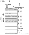
- FIG. 18 is a sectional view of an nin variable capacity device 500 in which a multi-period layer is formed in an i-layer.
- the variable capacity device 500 has a substrate 10 made of gallium arsenide (GaAs).
- GaAs buffer layer 12 of n-type conduction having a thickness generally of 0.3 ⁇ m and an electron concentration of 2 x 10 18 /cm 3 , is formed on the substrate 10.
- An n-Ga 0.51 In 0.49 P contact layer 14 of n-type conduction having a thickness generally of 0.13 ⁇ m and electron concentration of 2 x 10 18 /cm 3 , is formed on the buffer layer 12.
- n-Al 0.51 In 0.49 P n-layer 16 of n-type conduction having a thickness generally of 0.2 ⁇ m and an electron concentration of 1 x 10 18 /cm 3 , is formed on the contact layer 14.
- a non-doped i-layer 18 is formed on the n-layer 16.
- a Ga 0.51 In 0.49 P second contact layer 522 of n-type conduction having a thickness generally of 0.13 ⁇ m and an electron concentration of 2 x 10 18 /cm 3 , is formed on the n-layer 520.
- An n-GaAs first contact layer 524 of n-type conduction having a thickness generally of 0.06 ⁇ m and an electron concentration of 2 x 10 18 /cm 3 , is formed on the second contact layer 522.
- a 2 , ..., A 4 are formed like A 1 , and 4 multi-period layer units in total are formed in the i-layer 18.
- FIGS. 8A to 8C show a structure of the multi-period layer unit A 1 in detail.
- the first layer W has a thickness of 5 nm
- the second layer B has a thickness of 7 nm.
- a non-doped ⁇ layer made of Al 0.33 Ga 0.33 In 0.33 P is formed at each interface between the first layer W and the second layer B.
- Non-doped Al 0.51 In 0.49 P carrier confinement layers C 1 to C 3 having a thickness of 177 nm, is formed between any multi-period layer units A i and A i+1 , respectively.
- the second layers B which contact to the n-layer 16 and the p-layer 520 have a thickness of 0.05 ⁇ m, respectively.
- the substrate 10 has a diameter of 2.0 inches and the normal direction of its main surface is offset toward the [011] axis by 15 degree from the (100) plane, just as same as the substrate 10 of Example 1.
- the variable capacity device 500 was manufactured by gas source molecular beam epitaxial deposition (GS-MBE) as in Example 1.
- the variable capacity device 500 can be manufactured by metal organic chemical vapor deposition (MOCVD).
- FIG. 4A shows an electric potential gradient occurring in the i-layer 18 as an insulation layer on the condition that an external voltage is applied to the interface between the n-layer 520 and the n-layer 16 of the variable capacity device 500.
- the ⁇ layer is not shown in FIGS. 4A to 4C, it is present at each interface between the first layer W and the second layer B, as shown in FIGS. 8A to 8C.
- Each multi-period layer units A 1 to A 4 reflects electrons when the external voltage is in the range of 0 to V 1 as shown in FIG. 4A.
- electrons which exist in the i-layer 18 are not conducted in the i-layer and are confined in each carrier confinement layers C 1 to C 3 , respectively.
- an effective thickness of a depletion layer becomes smaller, and an electrostatic capacity between the electrodes 26 and 528 becomes larger.
- each multi-period layer units A 1 to A 4 reflects electrons is not satisfied. Accordingly, electrons are conducted and a electron concentration of each carrier confinement layers C 1 to C 3 is decreased. Because each carrier confinement layers C 1 to C 3 becomes a depletion layer, which means that equivalently the thickness of the depletion layer in the i-layer 18 becomes larger, the capacity of the variable capacity device 500 decreases. Thus by applying a larger applied voltage V, the capacity can be decreased.
- Capacity value with respect to an alternating current when a voltage V was applied as a bias voltage was measured by varying the respective value of the applied voltage V.
- FIG. 19 shows a result when the alternating currents are fixed at 100 kHz and 1 MHz, respectively.
- a characteristics X shows a curve when the alternating current is 1 MHz.
- a characteristics Y shows a curve when the alternating current is 100 kHz.
- a peak of capacity value of Y is obtained when the applied voltage V is 0.7 V.
- a characteristics Z shows a curve of a voltage-variable capacity device in the prior art. As shown in FIG. 19, it is obvious from the characteristics X and Y that a voltage-variation rate of capacity in the region over 0.8 V is improved compared with that of the prior art. And it is understood that a dynamic range of variable capacity is wider than that of the prior art.
- FIG. 20 is a sectional view of a pn - n variable capacity device 600 in which a multi-period layer is formed in an n - -type layer.
- the variable capacity device 600 has a GaAs substrate 10, an n-GaAs buffer layer 12, an n-Ga 0.51 In 0.49 P contact layer 14 of n-type conduction, and an n-Al 0.51 In 0.49 P n-layer 16, that are the same layers as those in the variable capacity device 500 in Example 3.
- the p-Al 0.51 In 0.49 P p-layer 20 of p-type conduction having a thickness generally of 0.2 ⁇ m and a hole concentration of 1 x 10 18 /cm 3 , is formed on the n - -layer 18.
- a p-Ga 0.51 In 0.49 P second contact layer 22 of p-type conduction having a thickness generally of 0.13 ⁇ m and a hole concentration of 2 x 10 18 /cm 3 , is formed on the p-layer 20.
- a p-GaAs first contact layer 24 of p-type conduction having a thickness generally of 0.06 ⁇ m and a hole concentration of 2 x 10 18 /cm 3 , is formed on the second contact layer 22.
- the n - -layer 18 has an electron concentration of 3 x 10 16 /cm 3 .
- a multi-period layer A 1 having a multi-quantum layer structure with 12 pairs of a Ga 0.51 In 0.49 P first layer W and an Al 0.51 In 0.49 P second layer B is formed in the n - -layer 18.
- a 2 , ..., A 5 are formed like A 1 , and 5 multi-period layer units in total are formed in the n - -layer 18.
- FIG. 8A shows a structure of the multi-period layer unit A 1 in detail.
- the first layer W has a thickness of 5 nm
- the second layer B has a thickness of 7 nm.
- a non-doped Al 0.51 In 0.49 P carrier confinement layers C 1 to C 4 each having a thickness of 14 nm, is formed between any multi-period layer units A i and A i+1 , respectively.
- the second layers B which contact to the n-layer 16 and the p-layer 20 have a thickness of 0.05 ⁇ m, respectively.
- the substrate 10 has a diameter of 2.0 inches and the normal direction of its main surface is offset toward the [011] axis by 15 degree from the (100) plane, just as same as the substrate 110 of Example 1.
- the variable capacity device 600 was manufactured by gas source molecular beam epitaxial deposition (GS-MBE) as in Example 1.
- the variable capacity device 500 can be manufactured by metal organic chemical vapor deposition (MOCVD).
- FIG. 6A shows an electric potential gradient occurring in the n - -layer 18 because of a higher resistivity compared with the p-layer 20 or the n-layer 16 on the condition that a backward voltage is applied to the interface between the p-layer 20 and the n-layer 16 of the variable capacity device 600.
- the ⁇ layer is not shown in FIGS. 6A to 6C, it is present at each interface between the first layer W and the second layer B, as shown in FIGS. 8A to 8C.
- FIGS. 8A to 8C Although only two carrier confinement layers C 1 and C 2 are shown in FIGS. 6A to 6C, four carrier confinement layers C 1 to C 4 exist as described above. Although only five pairs of layers in each of multi-period layer units are shown in FIGS.
- Each multi-period layer units A 1 to A 5 reflects electrons when an external voltage is in the range of 0 to V 1 as shown in FIG. 6A.
- electrons which exist in the n - layer 18 are not conducted in the n - layer 18 and are confined in each carrier confinement layers C 1 to C 4 , respectively.
- an effective thickness of a depletion layer becomes smaller, and an electrostatic capacity between the electrodes 26 and 28 becomes larger.
- each multi-period layer units A 1 to A 5 reflects electrons is not satisfied. Accordingly, electrons are conducted and an electron concentration of each carrier confinement layers C 1 to C 4 is decreased. Because each carrier confinement layers C 1 to C 4 becomes a depletion layer, which means that equivalently the thickness of the depletion layer in the n - -layer 18 becomes larger, the capacity of the variable capacity device 600 decreases. Thus by applying a larger applied voltage V, the capacity can be decreased.
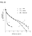
- a variable capacity device has the same structure as that of the variable capacity device 600 of FIG. 20.
- a thickness of each carrier confinement layers C 1 to C 4 is duplicated to 8 nm and a measured capacity is shown in FIG. 22. Comparing FIG. 22 with FIG. 21, a voltage-variation rate of capacity becomes smaller in accordance with a thickness of each carrier confinement layers C 1 to C 4 being larger. The dynamic range of capacity of both obtained devices are improved to be wider compared with that of the prior art.
- an interference effect of quantum-wave of carriers in the multi-period layer can be improved by forming a plural multi-period layers each having a carrier confinement layer, which has a wider band gap than the first layer, or by forming a plural multi-period layers each having a carrier confinement layer, which has a narrower band gap than the second layer.
- a multi-period layer in the present invention is not limited to a reflection of carriers.
- a ⁇ layer is formed in the device.
- the ⁇ layer improves the reflectivity of the device.
- the reflectivity can be obtained by a multi-period layer, the ⁇ layer is not necessarily needed.
- plural numbers of multi-period layers are connected in series, with a carrier confinement layer lying between each of the multi-period layers.
- a carrier confinement layer lying between each of the multi-period layers.
- an arbitrary pairs of a first layer and a second layer can be formed in the multi-period.
- an arbitrary numbers of carrier confinement layers can be formed in an arbitrary numbers of multi-period layers.
- the multi-period layer was made of ternary compounds including Ga 0.51 In 0.49 P and Al 0.51 In 0.49 P.
- the multi-period layer can be made of quaternary compounds such as Al x Ga y In 1-x-y P or Al x Ga y In 1-x-y As, selecting arbitrary composition ratio within the range of 0 ⁇ x ⁇ 1, 0 ⁇ y ⁇ 1, and 0 ⁇ x+y ⁇ 1.
- the multi-period layer can be made of group III-V compound semiconductor, group II-VI compound semiconductors, Si and Ge, and semiconductors of other hetero-material.
- the desirable compositions are as follows. Each combinations is represented by a composition of a layer having a wide band width / a layer having a narrow band width // a substrate. And x and y are arbitrary values wherein 0 ⁇ x ⁇ 1 and 0 ⁇ y ⁇ 1, as long as they are not specified.
- Plurality of multi-period layer units with a plural-layer structure, having plural periods of a pair of a first layer W and a second layer B are formed in a semiconductor device.
- the second layer B has wider band gap than the first layer W.
- a carrier confinement layer having a wider band width than the first layer W is formed at each interface of the multi-period layer units, and plurality of multi-period layer units are connected in series. Accordingly, a semiconductor device with a first structure is formed.
- Plurality of multi-period layer units with a plural-layer structure, having plural periods of a pair of a first layer W and a second layer B are formed in a semiconductor device.
- the second layer B has wider band gap than the first layer W.
- a carrier confinement layer having a narrower band width than the second layer B is formed at each interface of the multi-period layer units, and plurality of multi-period layer units are connected in series. Accordingly, a semiconductor device with a second structure is formed.
- the semiconductor device having the first structure can be effectively applied to a pin-type photodiode and a voltage-variable capacity, and the semiconductor device having the second structure can be effectively applied to a light-receiving device.
Landscapes
- Chemical & Material Sciences (AREA)
- Engineering & Computer Science (AREA)
- Nanotechnology (AREA)
- Physics & Mathematics (AREA)
- Life Sciences & Earth Sciences (AREA)
- Biophysics (AREA)
- Optics & Photonics (AREA)
- Crystallography & Structural Chemistry (AREA)
- Light Receiving Elements (AREA)
Applications Claiming Priority (2)
| Application Number | Priority Date | Filing Date | Title |
|---|---|---|---|
| JP10299507A JP2000124495A (ja) | 1998-10-21 | 1998-10-21 | キャリア閉込層を有した半導体素子 |
| JP29950798 | 1998-10-21 |
Publications (1)
| Publication Number | Publication Date |
|---|---|
| EP0996169A2 true EP0996169A2 (de) | 2000-04-26 |
Family
ID=17873486
Family Applications (1)
| Application Number | Title | Priority Date | Filing Date |
|---|---|---|---|
| EP99120752A Withdrawn EP0996169A2 (de) | 1998-10-21 | 1999-10-20 | Halbleiteranordnung mit einer Begrenzungsschicht |
Country Status (2)
| Country | Link |
|---|---|
| EP (1) | EP0996169A2 (de) |
| JP (1) | JP2000124495A (de) |
Families Citing this family (1)
| Publication number | Priority date | Publication date | Assignee | Title |
|---|---|---|---|---|
| CN102157596B (zh) * | 2011-03-18 | 2013-05-08 | 江苏大学 | 一种势垒型硅基薄膜半叠层太阳电池 |
-
1998
- 1998-10-21 JP JP10299507A patent/JP2000124495A/ja active Pending
-
1999
- 1999-10-20 EP EP99120752A patent/EP0996169A2/de not_active Withdrawn
Also Published As
| Publication number | Publication date |
|---|---|
| JP2000124495A (ja) | 2000-04-28 |
Similar Documents
| Publication | Publication Date | Title |
|---|---|---|
| US6603184B2 (en) | Double heterostructure photodiode with graded minority-carrier blocking structures | |
| US9178089B1 (en) | Strain-balanced extended-wavelength barrier detector | |
| US5077593A (en) | Dark current-free multiquantum well superlattice infrared detector | |
| KR100393461B1 (ko) | 이종접합에너지경사구조 | |
| US6326654B1 (en) | Hybrid ultraviolet detector | |
| US4679061A (en) | Superlattice photoconductor | |
| JPH065784B2 (ja) | アバランシエ光検出器 | |
| US6175123B1 (en) | Semiconductor devices with quantum-wave interference layers | |
| JP3287458B2 (ja) | 超高速・低電圧駆動アバランシェ増倍型半導体受光素子 | |
| Capasso | The channeling avalanche photodiode: A novel ultra-low-noise interdigitated pn junction detector | |
| US4486765A (en) | Avalanche photodetector including means for separating electrons and holes | |
| US7161170B1 (en) | Doped-absorber graded transition enhanced multiplication avalanche photodetector | |
| US6294795B1 (en) | Light-receiving device with quantum-wave interference layers | |
| US6188083B1 (en) | Diodes with quantum-wave interference layers | |
| EP0996169A2 (de) | Halbleiteranordnung mit einer Begrenzungsschicht | |
| US6331716B1 (en) | Variable capacity device with quantum-wave interference layers | |
| US6188082B1 (en) | Diodes with quantum-wave interference layers | |
| WO2003077283A2 (en) | Drift-dominated detector | |
| US6552412B2 (en) | Semiconductor device with quantum-wave interference layers | |
| US6818916B2 (en) | Light-receiving device with quantum-wave interference layers | |
| US6479842B1 (en) | Field effect transistor with a quantum-wave interference layer | |
| JPS6244867B2 (de) | ||
| JP2671569B2 (ja) | アバランシェフォトダイオード | |
| US20230114395A1 (en) | Photodetector and integrated circuit | |
| EP0996166A2 (de) | Halbleiteranordnungen mit einer Mehrfach-Quantenbarrierestruktur |
Legal Events
| Date | Code | Title | Description |
|---|---|---|---|
| PUAI | Public reference made under article 153(3) epc to a published international application that has entered the european phase |
Free format text: ORIGINAL CODE: 0009012 |
|
| AK | Designated contracting states |
Kind code of ref document: A2 Designated state(s): AT BE CH CY DE DK ES FI FR GB GR IE IT LI LU MC NL PT SE |
|
| AX | Request for extension of the european patent |
Free format text: AL;LT;LV;MK;RO;SI |
|
| STAA | Information on the status of an ep patent application or granted ep patent |
Free format text: STATUS: THE APPLICATION IS DEEMED TO BE WITHDRAWN |
|
| 18D | Application deemed to be withdrawn |
Effective date: 20040501 |