EP0996192A2 - Antenne réseau plane - Google Patents
Antenne réseau plane Download PDFInfo
- Publication number
- EP0996192A2 EP0996192A2 EP99308068A EP99308068A EP0996192A2 EP 0996192 A2 EP0996192 A2 EP 0996192A2 EP 99308068 A EP99308068 A EP 99308068A EP 99308068 A EP99308068 A EP 99308068A EP 0996192 A2 EP0996192 A2 EP 0996192A2
- Authority
- EP
- European Patent Office
- Prior art keywords
- antenna elements
- planar array
- patch antenna
- array antenna
- elements
- Prior art date
- Legal status (The legal status is an assumption and is not a legal conclusion. Google has not performed a legal analysis and makes no representation as to the accuracy of the status listed.)
- Granted
Links
Images


Classifications
-
- H—ELECTRICITY
- H01—ELECTRIC ELEMENTS
- H01Q—ANTENNAS, i.e. RADIO AERIALS
- H01Q13/00—Waveguide horns or mouths; Slot antennas; Leaky-waveguide antennas; Equivalent structures causing radiation along the transmission path of a guided wave
- H01Q13/08—Radiating ends of two-conductor microwave transmission lines, e.g. of coaxial lines, of microstrip lines
-
- H—ELECTRICITY
- H01—ELECTRIC ELEMENTS
- H01Q—ANTENNAS, i.e. RADIO AERIALS
- H01Q9/00—Electrically-short antennas having dimensions not more than twice the operating wavelength and consisting of conductive active radiating elements
- H01Q9/04—Resonant antennas
- H01Q9/0407—Substantially flat resonant element parallel to ground plane, e.g. patch antenna
-
- H—ELECTRICITY
- H01—ELECTRIC ELEMENTS
- H01Q—ANTENNAS, i.e. RADIO AERIALS
- H01Q21/00—Antenna arrays or systems
- H01Q21/06—Arrays of individually energised antenna units similarly polarised and spaced apart
- H01Q21/061—Two dimensional planar arrays
- H01Q21/065—Patch antenna array
-
- H—ELECTRICITY
- H01—ELECTRIC ELEMENTS
- H01Q—ANTENNAS, i.e. RADIO AERIALS
- H01Q21/00—Antenna arrays or systems
- H01Q21/24—Combinations of antenna units polarised in different directions for transmitting or receiving circularly and elliptically polarised waves or waves linearly polarised in any direction
Definitions
- the present invention relates to a planar array antenna which can be applied to a transmit/receive antenna used for a WLL (wireless local loop) terminal.
- WLL wireless local loop
- FIGS. 5A to 5C illustrate one example of a prior art planar array antenna of the above type.
- a plurality of (two in this example) patch antenna elements 101 and 102 are arrayed on a rectangular dielectric substrate 100.
- the elements 101 and 102 are coupled to each other by a feed line 103, while the element 102 is coupled to a feeding point 105 by a feed line 104.
- the feed lines 103 and 104 are each constituted of a strip line adhered onto the dielectric substrate 100.
- an electric power is applied, as a series feed, from the feeding point 105 to the patch antenna elements 101 and 102 through the feed lines 103 and 104.
- the planar array antenna so constituted is miniaturized as a whole by the dielectric effect of the dielectric substrate 100. Since, however, the antenna is decreased in gain due to a dielectric loss, a usable bandwidth of VSWR (voltage standing-wave ratio) is narrowed. Since, moreover, the plurality of patch antenna elements 101 and 102 are arrayed and an electric power is applied to these elements as a series feed, the following problem arises.
- the patch antenna elements 101 and 102 are difficult to arrange at the optimum interval under the influence of a so-called contraction rate due to the dielectric of the dielectric substrate 100. This problem will be described more specifically.
- the electrical length of the antenna is determined such that the length of each of the patch antenna elements 101 and 102 and the interval between them are both ⁇ /2 when the wavelength of transmitted/received wave is ⁇ .
- the contraction rate which is one of dielectric effects of the dielectric substrate 100, is taken into consideration in order to set the electrical length.
- the energy area of the patch antenna element 101 is S101 and that of the patch antenna element 102 is S102, these areas overlap each other to cause a region S103 shaded diagonally therein.
- the overlapped region S103 reduces the antenna efficiency and accordingly the maximum gain cannot be obtained under the influence of a dielectric loss.
- Teflon is used as the dielectric substrate 100, the gain falls within a range from 8dBi to 9dBi, which is about 30% lower than the maximum gain in the ideal status or in air.
- the object of the present invention is to provide a planer array antenna having the following advantages:
- planar array antenna of the present invention has the following feature in constitution.
- the other features will be clarified in the Description of the Invention.
- a planar array antenna comprises a ground plate formed of metallic material, a plurality of patch antenna elements supported on the ground plate by insulation spacers, respectively, and arrayed at a predetermined pitch, and a feed line for coupling adjacent antenna elements of the plurality of patch antenna elements.
- FIGS. 1A to 1C illustrate a planar array antenna according to an embodiment of the present invention.
- reference numeral 10 denotes a ground plate formed of metallic material such as brass.
- a plurality of (two in this embodiment) patch antenna elements 11 and 12, which are metal plates formed of the same brass, are supported on the ground plate 10 by means of insulation spacers 13 and 14, respectively.
- Reference numerals 15 and 16 indicate fixing screws for mounting and fixing the patch antenna elements 11 and 12 onto the ground plate 10.
- the insulation spacers 13 and 14 are each a cylinder (short cylinder in this embodiment) formed of resin such as polyacetal, polycarbonate, and ABS. These spacers each have a considerably small diameter D and an appropriate thickness T, with respect to the areas of the patch antenna elements 11 and 12, such that they can locally support the central parts of the elements 11 and 12.
- the electrical length is determined such that the length of each of the patch antenna elements 11 and 12 and the interval between them are both ⁇ /2 when the wavelength of transmitted/received wave is ⁇ .
- the elements 11 and 12 are connected to each other by means of a feed line 17 constituted of a strip line whose length is ⁇ /2 and whose resistance ranges from 100 ⁇ to 500 ⁇ .
- the strip line can be formed using a brass- or copper-made wire or plate.
- any contraction rate need not be considered in particular since there are no dielectric substrates. Consequently, the length of the feed line 17 or the actual physical distance R between the patch antenna elements 11 and 12 can be set equal to the length L of each of the elements 11 and 12. In other words, both the distance R and length L can be set to ⁇ /2.
- Points A and B are set on the patch antenna element 12. Since the side lobe of directivity is out of balance at the point B, the point A is regarded as a feeding point. As shown in FIG. 1B, a feeding pin 18 stands on the point A, a portion of the pin 18 which projects toward the back of the ground plate 10, is connected to a matching substrate 19 for correcting a reactance, and the matching substrate 19 is connected to a feeder 20.
- the patch antenna elements 11 and 12 of the present invention are formed on the ground plate 10 of metallic material and their central parts are locally supported by their respective insulation spacers 13 and 14 of short cylinders.
- the antenna elements 11 and 12 are coupled to each other by means of the feed line 17 of the wire or plate strip line such that the line acts as a bridge in the air.
- the dielectric-loss elements of the planar array antenna are only the ultrasmall-sized insulation spacers 13 and 14 supporting the patch antenna elements 11 and 12.
- the permittivity is ⁇ r related to the antenna gain becomes "1" which is close to that in air, with the result that the dielectric loss is very low and the gain is hardly decreased.
- the physical distance R between them is not influenced by the contraction rate due to a dielectric and, in other words, the distance R can be set to a length corresponding to ⁇ /2.
- the energy areas S11 and S12 of adjacent elements 11 and 12 can be prevented from overlapping when the element length and the element interval are set to the electrical length of ⁇ /2 as illustrated in FIG. 1C.
- the ideal array interval can be secured, so that the antenna efficiency is remarkably increased and the maximum antenna gain can be achieved.
- the gain of the two patch antenna elements 11 and 12 which was conventionally 8dBi to 9dBi, can be increased up to 12dBi or higher. If the number of patch antenna elements having the same structure is increased, the gain can be improved further. A usable bandwidth of VSWR can be broadened greatly.
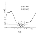
- FIG. 2 is a graph showing VSWR characteristics of the planar array antenna according to the embodiment of the present invention. As is apparent from FIG. 2, the bandwidth W1, which was conventionally 1.5%, is improved to 2.9% when VSWR is 1.5 or less, while the bandwidth W2, which was conventionally 2.8%, is improved to 5.3% when VSWR is 1.8 or less.
- FIG. 3 is a radiation-pattern view (beam width: 27.75 degrees) of the directivity of E-plane (electric-field plane) of the planar array antenna according to the embodiment of the present invention
- FIG. 4 is a radiation-pattern view (beam width: 61.50 degrees) of the directivity of H-plane (magnetic-field plane) of the planar array antenna.
- the directivity of both the E and H planes have good characteristics which are sufficiently in practical use.
- the planar array antenna of the embodiment of the present invention can be simplified and miniaturized as a whole. Since, furthermore, the ground plate 10 of metallic material is used as a base, the materials cost of the antenna becomes 10% to 20% lower than that of a conventional one using a dielectric substrate as a base. The antenna of the present invention can thus be manufactured at very low cost.
Landscapes
- Waveguide Aerials (AREA)
- Variable-Direction Aerials And Aerial Arrays (AREA)
Applications Claiming Priority (2)
| Application Number | Priority Date | Filing Date | Title |
|---|---|---|---|
| JP29679298 | 1998-10-19 | ||
| JP29679298A JP4121196B2 (ja) | 1998-10-19 | 1998-10-19 | 平板型アレイアンテナ |
Publications (3)
| Publication Number | Publication Date |
|---|---|
| EP0996192A2 true EP0996192A2 (fr) | 2000-04-26 |
| EP0996192A3 EP0996192A3 (fr) | 2003-03-19 |
| EP0996192B1 EP0996192B1 (fr) | 2004-09-22 |
Family
ID=17838202
Family Applications (1)
| Application Number | Title | Priority Date | Filing Date |
|---|---|---|---|
| EP99308068A Expired - Lifetime EP0996192B1 (fr) | 1998-10-19 | 1999-10-13 | Antenne réseau plane |
Country Status (8)
| Country | Link |
|---|---|
| US (1) | US6208298B1 (fr) |
| EP (1) | EP0996192B1 (fr) |
| JP (1) | JP4121196B2 (fr) |
| KR (1) | KR100592342B1 (fr) |
| AT (1) | ATE277431T1 (fr) |
| DE (1) | DE69920369T2 (fr) |
| ES (1) | ES2226296T3 (fr) |
| TW (1) | TW434941B (fr) |
Cited By (2)
| Publication number | Priority date | Publication date | Assignee | Title |
|---|---|---|---|---|
| EP1193794A3 (fr) * | 2000-09-26 | 2003-02-26 | Harada Industry Co., Ltd. | Dispositif d'antenne plane |
| EP2159876A1 (fr) * | 2008-08-28 | 2010-03-03 | Thales Nederland B.V. | Antenne de réseau comprenant un moyen pour établir des contacts galvaniques entre les éléments de son radiateur tout en permettant leur expansion thermique |
Families Citing this family (8)
| Publication number | Priority date | Publication date | Assignee | Title |
|---|---|---|---|---|
| US6567047B2 (en) * | 2000-05-25 | 2003-05-20 | Tyco Electronics Logistics Ag | Multi-band in-series antenna assembly |
| US6362789B1 (en) * | 2000-12-22 | 2002-03-26 | Rangestar Wireless, Inc. | Dual band wideband adjustable antenna assembly |
| JP3820223B2 (ja) * | 2003-01-14 | 2006-09-13 | 株式会社国際電気通信基礎技術研究所 | 平面アレーアンテナ装置 |
| KR20070093094A (ko) * | 2004-12-06 | 2007-09-17 | 코닌클리케 필립스 일렉트로닉스 엔.브이. | 전도성 브리지에 의해 연결된 전도면들을 갖는 안테나 |
| JP4224055B2 (ja) * | 2005-12-19 | 2009-02-12 | 三星電子株式会社 | アンテナ |
| US8059034B2 (en) * | 2008-07-24 | 2011-11-15 | The United States of America as resprented by the Secretary of the Army | High efficiency and high power patch antenna and method of using |
| JP6525249B2 (ja) * | 2015-03-20 | 2019-06-05 | カシオ計算機株式会社 | アンテナ装置及び電子機器 |
| JP6893767B2 (ja) * | 2016-09-23 | 2021-06-23 | 日本ピラー工業株式会社 | 平面アンテナ及びアンテナ装置 |
Family Cites Families (8)
| Publication number | Priority date | Publication date | Assignee | Title |
|---|---|---|---|---|
| US4117489A (en) * | 1975-04-24 | 1978-09-26 | The United States Of America As Represented By The Secretary Of The Navy | Corner fed electric microstrip dipole antenna |
| US4464663A (en) * | 1981-11-19 | 1984-08-07 | Ball Corporation | Dual polarized, high efficiency microstrip antenna |
| JPH04186904A (ja) * | 1990-11-21 | 1992-07-03 | Hitachi Chem Co Ltd | 平面アンテナ |
| US5309164A (en) * | 1992-04-13 | 1994-05-03 | Andrew Corporation | Patch-type microwave antenna having wide bandwidth and low cross-pol |
| CA2117223A1 (fr) * | 1993-06-25 | 1994-12-26 | Peter Mailandt | Antenne a reseau de plaques microruban |
| SE504951C2 (sv) * | 1995-09-29 | 1997-06-02 | Ericsson Telefon Ab L M | Anordning vid antennenheter |
| US5892482A (en) * | 1996-12-06 | 1999-04-06 | Raytheon Company | Antenna mutual coupling neutralizer |
| US5896107A (en) * | 1997-05-27 | 1999-04-20 | Allen Telecom Inc. | Dual polarized aperture coupled microstrip patch antenna system |
-
1998
- 1998-10-19 JP JP29679298A patent/JP4121196B2/ja not_active Expired - Fee Related
-
1999
- 1999-10-13 ES ES99308068T patent/ES2226296T3/es not_active Expired - Lifetime
- 1999-10-13 DE DE69920369T patent/DE69920369T2/de not_active Expired - Fee Related
- 1999-10-13 EP EP99308068A patent/EP0996192B1/fr not_active Expired - Lifetime
- 1999-10-13 AT AT99308068T patent/ATE277431T1/de not_active IP Right Cessation
- 1999-10-14 TW TW088117907A patent/TW434941B/zh not_active IP Right Cessation
- 1999-10-18 US US09/420,114 patent/US6208298B1/en not_active Expired - Fee Related
- 1999-10-19 KR KR1019990045209A patent/KR100592342B1/ko not_active Expired - Fee Related
Cited By (4)
| Publication number | Priority date | Publication date | Assignee | Title |
|---|---|---|---|---|
| EP1193794A3 (fr) * | 2000-09-26 | 2003-02-26 | Harada Industry Co., Ltd. | Dispositif d'antenne plane |
| US6731243B2 (en) | 2000-09-26 | 2004-05-04 | Harada Industry Co., Ltd | Planar antenna device |
| EP2159876A1 (fr) * | 2008-08-28 | 2010-03-03 | Thales Nederland B.V. | Antenne de réseau comprenant un moyen pour établir des contacts galvaniques entre les éléments de son radiateur tout en permettant leur expansion thermique |
| NL1035878C (en) * | 2008-08-28 | 2010-03-11 | Thales Nederland Bv | An array antenna comprising means to establish galvanic contacts between its radiator elements while allowing for their thermal expansion. |
Also Published As
| Publication number | Publication date |
|---|---|
| KR100592342B1 (ko) | 2006-06-21 |
| EP0996192B1 (fr) | 2004-09-22 |
| ES2226296T3 (es) | 2005-03-16 |
| ATE277431T1 (de) | 2004-10-15 |
| US6208298B1 (en) | 2001-03-27 |
| JP2000124734A (ja) | 2000-04-28 |
| JP4121196B2 (ja) | 2008-07-23 |
| DE69920369T2 (de) | 2005-09-29 |
| EP0996192A3 (fr) | 2003-03-19 |
| DE69920369D1 (de) | 2004-10-28 |
| KR20000029161A (ko) | 2000-05-25 |
| TW434941B (en) | 2001-05-16 |
Similar Documents
| Publication | Publication Date | Title |
|---|---|---|
| CA2439343C (fr) | Antenne papillon a fentes croisees | |
| EP1950830A1 (fr) | Antenne à mode fente à double polarisation et procédés associés | |
| US5070340A (en) | Broadband microstrip-fed antenna | |
| US11183775B2 (en) | Base station antennas having parasitic assemblies for improving cross-polarization discrimination performance | |
| EP0856909A1 (fr) | Antennes cellulaires | |
| JPH10150319A (ja) | 反射板付ダイポ−ルアンテナ | |
| US20050110699A1 (en) | Dual polarized three-sector base station antenna with variable beam tilt | |
| US7764242B2 (en) | Broadband antenna system | |
| GB2333400A (en) | Base station antenna for dual polarization | |
| WO1991012637A1 (fr) | Antenne | |
| EP0996192B1 (fr) | Antenne réseau plane | |
| US7339543B2 (en) | Array antenna with low profile | |
| KR19980069830A (ko) | 마이크로스트립 급전선을 갖는 로그 주기 다이폴 안테나 | |
| US20050162333A1 (en) | UHF broadband antenna | |
| NO335280B1 (no) | Mikrostriplogperiodisk antennegruppe med jordet semikoplanar bølgeleder-til-mikrostrip-linjeovergang | |
| EP0487053A1 (fr) | Antenne | |
| US6016127A (en) | Traveling wave antenna | |
| JP3804878B2 (ja) | 偏波共用アンテナ | |
| JP3782278B2 (ja) | 偏波共用アンテナのビーム幅制御方法 | |
| TW201208197A (en) | High gain loop array antenna system and electronic device | |
| KR100577342B1 (ko) | 캐비티 슬롯 어레이 형태의 방사구조를 갖는 위성방송수신용 고이득 슬롯 배열 안테나 | |
| JP2006014152A (ja) | 平面アンテナ | |
| Lee et al. | Broadband high‐efficiency microstrip antenna array with corporate‐series‐feed | |
| Loffler et al. | Low-cost X-polarised broadband PCS antenna with low cross-polarisation level | |
| JP3243001B2 (ja) | 進行波形アンテナ |
Legal Events
| Date | Code | Title | Description |
|---|---|---|---|
| PUAI | Public reference made under article 153(3) epc to a published international application that has entered the european phase |
Free format text: ORIGINAL CODE: 0009012 |
|
| 17P | Request for examination filed |
Effective date: 19991103 |
|
| AK | Designated contracting states |
Kind code of ref document: A2 Designated state(s): AT BE CH CY DE DK ES FI FR GB GR IE IT LI LU MC NL PT SE |
|
| AX | Request for extension of the european patent |
Free format text: AL;LT;LV;MK;RO;SI |
|
| PUAL | Search report despatched |
Free format text: ORIGINAL CODE: 0009013 |
|
| AK | Designated contracting states |
Kind code of ref document: A3 Designated state(s): AT BE CH CY DE DK ES FI FR GB GR IE IT LI LU MC NL PT SE Designated state(s): AT BE CH CY DE DK ES FI FR GB GR IE IT LI LU MC NL PT SE |
|
| AX | Request for extension of the european patent |
Extension state: AL LT LV MK RO SI |
|
| 17Q | First examination report despatched |
Effective date: 20030702 |
|
| AKX | Designation fees paid |
Designated state(s): AT BE CH CY DE DK ES FI FR GB GR IE IT LI LU MC NL PT SE |
|
| GRAP | Despatch of communication of intention to grant a patent |
Free format text: ORIGINAL CODE: EPIDOSNIGR1 |
|
| GRAS | Grant fee paid |
Free format text: ORIGINAL CODE: EPIDOSNIGR3 |
|
| GRAA | (expected) grant |
Free format text: ORIGINAL CODE: 0009210 |
|
| AK | Designated contracting states |
Kind code of ref document: B1 Designated state(s): AT BE CH CY DE DK ES FI FR GB GR IE IT LI LU MC NL PT SE |
|
| PG25 | Lapsed in a contracting state [announced via postgrant information from national office to epo] |
Ref country code: LI Free format text: LAPSE BECAUSE OF FAILURE TO SUBMIT A TRANSLATION OF THE DESCRIPTION OR TO PAY THE FEE WITHIN THE PRESCRIBED TIME-LIMIT Effective date: 20040922 Ref country code: FI Free format text: LAPSE BECAUSE OF FAILURE TO SUBMIT A TRANSLATION OF THE DESCRIPTION OR TO PAY THE FEE WITHIN THE PRESCRIBED TIME-LIMIT Effective date: 20040922 Ref country code: CY Free format text: LAPSE BECAUSE OF FAILURE TO SUBMIT A TRANSLATION OF THE DESCRIPTION OR TO PAY THE FEE WITHIN THE PRESCRIBED TIME-LIMIT Effective date: 20040922 Ref country code: CH Free format text: LAPSE BECAUSE OF FAILURE TO SUBMIT A TRANSLATION OF THE DESCRIPTION OR TO PAY THE FEE WITHIN THE PRESCRIBED TIME-LIMIT Effective date: 20040922 Ref country code: BE Free format text: LAPSE BECAUSE OF FAILURE TO SUBMIT A TRANSLATION OF THE DESCRIPTION OR TO PAY THE FEE WITHIN THE PRESCRIBED TIME-LIMIT Effective date: 20040922 Ref country code: AT Free format text: LAPSE BECAUSE OF FAILURE TO SUBMIT A TRANSLATION OF THE DESCRIPTION OR TO PAY THE FEE WITHIN THE PRESCRIBED TIME-LIMIT Effective date: 20040922 |
|
| REG | Reference to a national code |
Ref country code: GB Ref legal event code: FG4D |
|
| PGFP | Annual fee paid to national office [announced via postgrant information from national office to epo] |
Ref country code: ES Payment date: 20040923 Year of fee payment: 6 |
|
| REG | Reference to a national code |
Ref country code: SE Ref legal event code: TRGR |
|
| PGFP | Annual fee paid to national office [announced via postgrant information from national office to epo] |
Ref country code: NL Payment date: 20040930 Year of fee payment: 6 Ref country code: FR Payment date: 20040930 Year of fee payment: 6 |
|
| REG | Reference to a national code |
Ref country code: CH Ref legal event code: EP |
|
| PG25 | Lapsed in a contracting state [announced via postgrant information from national office to epo] |
Ref country code: LU Free format text: LAPSE BECAUSE OF NON-PAYMENT OF DUE FEES Effective date: 20041013 Ref country code: IE Free format text: LAPSE BECAUSE OF NON-PAYMENT OF DUE FEES Effective date: 20041013 |
|
| REG | Reference to a national code |
Ref country code: IE Ref legal event code: FG4D |
|
| REF | Corresponds to: |
Ref document number: 69920369 Country of ref document: DE Date of ref document: 20041028 Kind code of ref document: P |
|
| PG25 | Lapsed in a contracting state [announced via postgrant information from national office to epo] |
Ref country code: MC Free format text: LAPSE BECAUSE OF NON-PAYMENT OF DUE FEES Effective date: 20041031 |
|
| PGFP | Annual fee paid to national office [announced via postgrant information from national office to epo] |
Ref country code: SE Payment date: 20041116 Year of fee payment: 6 |
|
| PG25 | Lapsed in a contracting state [announced via postgrant information from national office to epo] |
Ref country code: GR Free format text: LAPSE BECAUSE OF FAILURE TO SUBMIT A TRANSLATION OF THE DESCRIPTION OR TO PAY THE FEE WITHIN THE PRESCRIBED TIME-LIMIT Effective date: 20041222 Ref country code: DK Free format text: LAPSE BECAUSE OF FAILURE TO SUBMIT A TRANSLATION OF THE DESCRIPTION OR TO PAY THE FEE WITHIN THE PRESCRIBED TIME-LIMIT Effective date: 20041222 |
|
| PGFP | Annual fee paid to national office [announced via postgrant information from national office to epo] |
Ref country code: DE Payment date: 20041223 Year of fee payment: 6 |
|
| REG | Reference to a national code |
Ref country code: ES Ref legal event code: FG2A Ref document number: 2226296 Country of ref document: ES Kind code of ref document: T3 |
|
| REG | Reference to a national code |
Ref country code: CH Ref legal event code: PL |
|
| ET | Fr: translation filed | ||
| REG | Reference to a national code |
Ref country code: IE Ref legal event code: MM4A |
|
| PLBE | No opposition filed within time limit |
Free format text: ORIGINAL CODE: 0009261 |
|
| STAA | Information on the status of an ep patent application or granted ep patent |
Free format text: STATUS: NO OPPOSITION FILED WITHIN TIME LIMIT |
|
| 26N | No opposition filed |
Effective date: 20050623 |
|
| PG25 | Lapsed in a contracting state [announced via postgrant information from national office to epo] |
Ref country code: IT Free format text: LAPSE BECAUSE OF NON-PAYMENT OF DUE FEES Effective date: 20051013 |
|
| PG25 | Lapsed in a contracting state [announced via postgrant information from national office to epo] |
Ref country code: SE Free format text: LAPSE BECAUSE OF NON-PAYMENT OF DUE FEES Effective date: 20051014 Ref country code: ES Free format text: LAPSE BECAUSE OF NON-PAYMENT OF DUE FEES Effective date: 20051014 |
|
| PG25 | Lapsed in a contracting state [announced via postgrant information from national office to epo] |
Ref country code: NL Free format text: LAPSE BECAUSE OF NON-PAYMENT OF DUE FEES Effective date: 20060501 |
|
| PG25 | Lapsed in a contracting state [announced via postgrant information from national office to epo] |
Ref country code: DE Free format text: LAPSE BECAUSE OF NON-PAYMENT OF DUE FEES Effective date: 20060503 |
|
| EUG | Se: european patent has lapsed | ||
| PG25 | Lapsed in a contracting state [announced via postgrant information from national office to epo] |
Ref country code: FR Free format text: LAPSE BECAUSE OF NON-PAYMENT OF DUE FEES Effective date: 20060630 |
|
| NLV4 | Nl: lapsed or anulled due to non-payment of the annual fee |
Effective date: 20060501 |
|
| REG | Reference to a national code |
Ref country code: FR Ref legal event code: ST Effective date: 20060630 |
|
| REG | Reference to a national code |
Ref country code: ES Ref legal event code: FD2A Effective date: 20051014 |
|
| PG25 | Lapsed in a contracting state [announced via postgrant information from national office to epo] |
Ref country code: PT Free format text: LAPSE BECAUSE OF NON-PAYMENT OF DUE FEES Effective date: 20050222 |
|
| PGFP | Annual fee paid to national office [announced via postgrant information from national office to epo] |
Ref country code: GB Payment date: 20071010 Year of fee payment: 9 |
|
| GBPC | Gb: european patent ceased through non-payment of renewal fee |
Effective date: 20081013 |
|
| PG25 | Lapsed in a contracting state [announced via postgrant information from national office to epo] |
Ref country code: GB Free format text: LAPSE BECAUSE OF NON-PAYMENT OF DUE FEES Effective date: 20081013 |