EP0996196A2 - Verbinder mit Anschlüssen mit verbesserten Lötanschlussstücken - Google Patents
Verbinder mit Anschlüssen mit verbesserten Lötanschlussstücken Download PDFInfo
- Publication number
- EP0996196A2 EP0996196A2 EP99113363A EP99113363A EP0996196A2 EP 0996196 A2 EP0996196 A2 EP 0996196A2 EP 99113363 A EP99113363 A EP 99113363A EP 99113363 A EP99113363 A EP 99113363A EP 0996196 A2 EP0996196 A2 EP 0996196A2
- Authority
- EP
- European Patent Office
- Prior art keywords
- terminal
- segment
- hole
- narrowed
- centerline
- Prior art date
- Legal status (The legal status is an assumption and is not a legal conclusion. Google has not performed a legal analysis and makes no representation as to the accuracy of the status listed.)
- Withdrawn
Links
Images



Classifications
-
- H—ELECTRICITY
- H01—ELECTRIC ELEMENTS
- H01R—ELECTRICALLY-CONDUCTIVE CONNECTIONS; STRUCTURAL ASSOCIATIONS OF A PLURALITY OF MUTUALLY-INSULATED ELECTRICAL CONNECTING ELEMENTS; COUPLING DEVICES; CURRENT COLLECTORS
- H01R12/00—Structural associations of a plurality of mutually-insulated electrical connecting elements, specially adapted for printed circuits, e.g. printed circuit boards [PCB], flat or ribbon cables, or like generally planar structures, e.g. terminal strips, terminal blocks; Coupling devices specially adapted for printed circuits, flat or ribbon cables, or like generally planar structures; Terminals specially adapted for contact with, or insertion into, printed circuits, flat or ribbon cables, or like generally planar structures
- H01R12/50—Fixed connections
- H01R12/51—Fixed connections for rigid printed circuits or like structures
- H01R12/55—Fixed connections for rigid printed circuits or like structures characterised by the terminals
- H01R12/58—Fixed connections for rigid printed circuits or like structures characterised by the terminals terminals for insertion into holes
-
- H—ELECTRICITY
- H01—ELECTRIC ELEMENTS
- H01R—ELECTRICALLY-CONDUCTIVE CONNECTIONS; STRUCTURAL ASSOCIATIONS OF A PLURALITY OF MUTUALLY-INSULATED ELECTRICAL CONNECTING ELEMENTS; COUPLING DEVICES; CURRENT COLLECTORS
- H01R12/00—Structural associations of a plurality of mutually-insulated electrical connecting elements, specially adapted for printed circuits, e.g. printed circuit boards [PCB], flat or ribbon cables, or like generally planar structures, e.g. terminal strips, terminal blocks; Coupling devices specially adapted for printed circuits, flat or ribbon cables, or like generally planar structures; Terminals specially adapted for contact with, or insertion into, printed circuits, flat or ribbon cables, or like generally planar structures
- H01R12/70—Coupling devices
- H01R12/71—Coupling devices for rigid printing circuits or like structures
- H01R12/72—Coupling devices for rigid printing circuits or like structures coupling with the edge of the rigid printed circuits or like structures
- H01R12/721—Coupling devices for rigid printing circuits or like structures coupling with the edge of the rigid printed circuits or like structures cooperating directly with the edge of the rigid printed circuits
Definitions
- the present invention relates to electrical connectors for mounting to printed circuit boards, and more particularly to an improved connector having terminals with improved solder tails.
- Devices such as computers using printed circuit boards are exhibiting increasing circuit densities and are operating at increasing frequencies. For example, the speeds of high frequency digital signals traveling between a computer motherboard and densely populated memory module printed circuit cards on an associated circuit board are becoming higher.
- US-A-5,161,987 discloses an electrical connector having a ground bus with a plurality of solder tails. A row of signal contacts is located on each side of the ground bus.
- US-A-5,162,002 discloses a card edge connector with spatially overlapped terminals having relatively shorter and relatively longer contact elements.
- This connector has important advantages such as reducing the peak card insertion force, but has electrical characteristics that are not optimized for higher speed digital signals.
- US-A-5,192,220 discloses a dual readout socket wherein crosstalk is reduced by increasing the space between connectors. This approach defeats the goal of increased circuit density.
- US-A-5,259,768 discloses an electrical connector having ground terminals with significantly larger surface areas than the signal terminals.
- the ground and signal terminals alternate, and the shadowing effect of the ground terminals reduces crosstalk.
- the ground terminals have both solder tails and grounding feet to reduce impedance generally, while non-functional stubs are sized to provide a specifically desired impedance.
- US-A-5,259,793 discloses an edge connector with terminals arranged in an alternating array along the circuit card insertion slot. Circuit density is diminished because of the alternating array.
- US-A-5,309,630 discloses an electrical connector wherein a desired impedance is obtained by selecting terminals having anchoring portions sized to correspond to the desired impedance.
- Signal and ground terminals may alternate, and at least the ground terminals are provided with two feet to reduce impedance.
- US-A-5,580,257 discloses a connector in which enlarged ground terminals are adjacent to pairs of signal terminals to reduce crosstalk. Although this arrangement has advantages, three different terminal shapes are required, and the operation of assembling terminals into the connector housing is complex.
- US-A-5,654,878 discloses a terminal tail having a reduced-width portion wherein parallel edges provide dual alignment positioning allowance on opposite sides of the tip of the solder tail for facilitating insertion thereof into a through hole.
- US-A-5,409,399 discloses solder tails having curved sections for providing transverse offset relative to the centerlines of the solder tails.
- An object of the present invention is to provide an improved connector.
- Other objects are to provide a connector with low inductance that can achieve an impedance match with associated circuit assemblies; to provide a connector having minimum cross talk between signal circuits; to provide a connector having high circuit density; to provide a connector that is robust although small; to provide a mechanically and electrically reliable connector that can be manufactured and assembled inexpensively; to provide a connector having a dense arrangement of board contacts while deterring solder bridging; and to provide an improved connector overcoming disadvantages of connectors used in the past.
- a edge card-type electrical connector for connecting a circuit card having opposed surfaces with conductive pads thereon to a circuit board having top and bottom surfaces and conductive regions on at least one of the top and bottom surfaces, at least one of the conductive regions being a through hole.
- the connector includes a dielectric housing having a longitudinal slot for receiving the circuit card therein and a plurality of terminal receiving cavities extending perpendicularly to and intersecting the slot.
- the connector further includes a signal terminal in one of the terminal receiving cavities.
- the signal terminal has a body portion, a contact arm extending from the body portion for contacting one of the conductive pads on the circuit card, a retention arm extending from the body portion for retaining the terminal in the cavity, and a board contact extending from the body portion to the conductive region of the circuit board.
- the connector further includes a reference or ground terminal in another of the terminal receiving cavities.
- the ground terminal has a body portion, a contact arm extending from the body portion for contacting one of the conductive pads on the circuit card, a retention section for retaining the terminal in the cavity, and a board contact extending from the body portion to the conductive region of the circuit board.
- One of the board contacts of one of the terminals is a through hole-type tail for extending through the through hole.
- the tail includes a full segment and an abutting narrowed segment, each segment having edges and a centerline generally perpendicular to the board.
- the centerline of the narrowed segment is offset from the centerline of the full segment, and the abutting segments abut between the top and bottom surfaces of the board when the tail is extending through the through hole.
- FIG. 1 there is illustrated a circuit assembly generally designated as 10 and including three card edge connectors, each generally designated as 12, constructed in accordance with the principles of the present invention.
- the circuit assembly 10 includes a printed circuit board 14, for example, a computer motherboard.
- the card edge connectors 12 are mounted on the circuit board 14 and removably receive printed circuit cards 16, for example, memory modules with random access memory available to the motherboard 14.
- the card edge connector provides circuit paths so that power, ground and digital signals can be transferred between the circuit board 14 and the circuit cards 16.
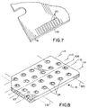
- the pertinent structure of the first electrical component, preferably circuit card 16, and the second electrical component, preferably circuit board 14, are shown in preferred embodiments in FIGS. 7 and 8, respectively.
- the card 16, of which a fragment is seen in FIG. 7, includes a leading or mating edge 18 that mates with the card edge connector 12.
- a series of conductive contact pads 20 is provided on both opposed surfaces of the card 16 substantially along the mating edge 18.
- Conductive traces on the card 16 provide power, ground and signal paths leading from the contact pads 20 to components (not shown) that are mounted on the card 16.
- FIG. 8 A fragment of the circuit board 14 is shown in FIG. 8.
- the upper surface 22 (or mating surface) of the board includes an array of conductive regions 24 which preferably extend to the bottom surface 23 (or remote surface) of the board 14.
- the conductive regions 24 are plated through holes (seen in cross-section in FIG. 10).
- Circuit traces in or on the circuit board 14 provide power, ground and signal paths from the conductive regions 24 to other components (not shown) mounted on the circuit board.
- the card edge connector 12 includes an elongated housing 26 made of an electrically insulating material such as a molded high temperature thermoplastic, such as liquid crystal polymer plastic.
- the housing has a top wall 28, a bottom wall 30 and opposed side walls 32.
- Housing end posts 37 and latches 38 may be provided at the ends of the housing 26, and hold downs 36 are generally known in the art and may be used to mechanically attach the housing 26 to the circuit board 14.
- the bottom wall 30 includes stand off projections 40 for maintaining a space between the bottom wall 30 and the top surface 22 (FIG. 1) of the circuit board 14.
- Numerous terminal receiving cavities 44 (FIG. 4) and 46 (FIG. 5) are provided in the housing 26. In a preferred embodiment of the invention, there may be over fifty cavities 44 and a similar number of cavities 46. Every cavity 44 is immediately adjacent to a cavity 46, and in the preferred embodiment of the invention, the cavities 44 and 46 alternate in position along of the length of the housing 26.
- the cavities 44 and 46 are separated by dielectric separator walls 48 which are integral members of the housing 26 and extend transversely or perpendicular to the slot 34 between the side walls 32.
- the cavities 44 and 46 intersect and extend to both opposed sides of the slot 34.
- the bottom of the slot 34 has a stop surface 50 defined in part by the separator walls 48 and by spacers 54 in the cavities 44 and terminal retention walls 56 in the cavities 46.
- the separator walls 48 are connected across cavities 44 by spacer 54 that extends only slightly downward from the stop surface 50 of slot 34.
- separator walls 48 are connected across cavities 46 by terminal retention walls 56 that extend downward from the stop surface of slot 34 substantially to the bottom of the housing 26.
- the side walls of the slot 34 are defined by the inner edges of comb-like upper portions 48a of the separator walls 48.
- the lower portions of the cavities 44 and 46 have opposed internal side walls 58.
- Each cavity 44 and 46 has an open bottom through which terminals may be inserted into the cavities.
- Reference terminals 60 are mounted in the cavities 44.
- the reference terminals generally provide ground or power connections between the circuit board 14 and the circuit card 16.
- Signal terminals 62 are mounted in the cavities 46.
- the signal terminals generally provide a circuit path for the transmission of alternating current, digital or other signals, typically high speed digital signals, between the circuit board 14 and the circuit card 16.
- the reference terminals 60 are all identical to one another and the signal terminals 62 are all identical to one another.
- the terminals 60 and 62 are flat, planar bodies of metal of uniform thickness, preferably made by stamping from metal sheet stock without any other forming or bending operations. This provides a more efficient manufacturing operation and a sturdier and more reliable terminal in comparison with electrical connectors having terminals that are both stamped and formed.
- the terminals 60 and 62 are stamped of phosphor bronze and plated with tin and lead over nickel, with selective gold plating at electrical contact areas, though other alloys or conductive materials may be used.
- the terminal 60 of the illustrated embodiment (also partially seen in FIG. 6) includes a generally rectangular, planar, plate like body 64 having upwardly extending retention arms 66 at both ends.
- the arms 66 have barbs 68 that engage the internal side walls 58 and resist removal of the terminal 60 after the terminal 60 is loaded into the cavity 44 through the bottom wall 30.
- the reference terminal 60 extends across the full width of the cavity 44 and extends to both sides of the slot 34. Other means for retention of the terminal 60, including ones lacking separate arms, are contemplated within the invention.
- a pair of spaced apart board contacts 72 extend downward from the body 64. These contacts are received in the plated through hole conductive regions 24 of the circuit board 14 to connect the terminal 60 to the circuit board.
- the use of two spaced board contacts for the single reference terminal 60 results in parallel redundant circuit paths and low inductance.
- a pair of opposed spring arms 74 extend upward from the body 64.
- Each spring arm 74 includes a flexible beam with a vertical portion 76 and an inwardly sloped portion 78.
- the end of the spring arm 74 includes a large segment 80 defining a lead-in surface 82 and a contact region 84.
- Each signal terminal 62 includes a generally rectangular, planar, plate like body 86 having upwardly extending retention arms 88 at both ends.
- the arms 88 have barbs 90 that retain the terminals 62 in the cavity 46.
- the arms 88 and barbs 90 engage the internal side walls 58.
- the arms 88 and barbs 90 engage opposite sides of the retention wall 56.
- means for retention of the signal terminal within the cavity other than retention arms are considered to be within the scope of the invention.
- a board contact 92 extends downward from the body 86 of each of the terminals 62 in the cavity 46. These contacts 92 are received in the plated through conductive regions 24 of the circuit board 14 to connect the terminals 62 to the circuit board 14. The conductive regions 24 connected to the signal terminals 62 are used to communicate AC signals such as high frequency digital signals between the circuit board 14 and the circuit card 16.
- the board contacts 92 are transversely offset from the reference terminal board contacts 72 in a staggered pattern (best seen in FIG. 8).
- a spring arm 94 extends upward from each of the bodies 86.
- Each spring arm 94 includes a flexible beam with a vertical portion 96 and an inwardly sloped portion 98.
- the end of the spring arm 94 includes a lead-in surface 100 and a contact region 102.
- the two identical signal terminals 62 are loaded into opposite sides of the cavity 46 in reversed positions relative to one another.
- the two terminals 62 are at opposite sides of the slot 34, and because of the reverse orientation, the two opposed spring arms 94 slope toward one another at opposite sides of the slot 34.
- the connector 12 of the present invention includes numerous terminal sets generally designated as 104, each including closely spaced and interfacing reference and signal terminals 60 and 62.
- One of these many terminal sets 104 is shown in FIG. 6 with the housing 26 omitted to reveal more of the structure of the terminal set.
- each set 104 includes a single reference terminal 60 and an opposed pair of signal terminals 62, but principles of the invention can apply to other arrangements, including where two reference and two signal terminals or one reference and one signal terminal are included in each set.
- the reference terminal cavities 44 alternate with the signal terminal cavities 46, but there could be other configurations such as two adjacent signal terminal cavities 44 between each pair of reference terminal cavities.
- each terminal set 104 the reference terminal 60 is parallel to and close to the pair of signal terminals 62.
- the reference terminal 60 substantially entirely overlies or shadows the signal terminals 62.
- the reference terminal body 64 entirely overlies the signal terminal bodies 86.
- the reference terminal body is enlarged beyond the extent of the signal terminal bodies 86 by the provision of the central span portion 70 and by downwardly extending the body 64 at the bases of the board contacts 72.
- the signal terminal inner retention arms 88 are overlaid by the retention arms 66 and by the span portion 70.
- the signal terminal contact beams 74 are overlaid by the reference terminal contact beams 94 except for the small contact regions 102.
- the enlarged segments 80 of the reference terminal contact arms 74 provide a large surface area overlying the ends of the signal terminal contact arms 94. Because these segments are larger than required for the conventional mechanical and electrical functions of the contact arms 74, they are defined as "oversize”.
- the oversize segments 80 provide several important functions. They increase coupling to the signal terminals 62 without significantly adding mass to functional parts of the terminal and possibly impeding mechanical operation. They provide a sturdy and rugged card lead-in area.
- the use of numerous such reference terminals 60 all having oversize segments in a symmetrical array at both sides of the circuit card 16 provides increased electrostatic shielding of circuits on both sides of the circuit card 16.
- the size of the segments 80 can be changed to adjust terminal impedance without interfering with the operation of the terminal.
- the segments could be reduced in length in accordance with the invention.
- the resulting terminal would have an impedance different from a terminal as illustrated with larger segments 80.
- other sections of the terminal may need to be correspondingly resized, this feature permits the terminal to be tailored or tuned to specific impedance requirements without interfering with the mechanical function of the terminal.
- the reference terminal contact regions 84 are at a higher elevation than the signal terminal contact regions 102.
- the mating edge 18 of the circuit card 16 When the mating edge 18 of the circuit card 16 is inserted into the slot 34, it first contacts the reference terminal contact arms 74 and reacts against the lead-in surfaces 82 to resiliently deflect or separate the arms 74. Thereafter, the mating card edge 18 contacts the signal terminal lead-in surfaces 100 and deflects or separates the signal terminal contact arms 94. The peak insertion force is reduced by separating these two contact engagement actions.
- FIG. 8 illustrates a fragmentary portion of the circuit board 14 showing the array of plated through hole conductive regions 24 through which extend board contacts 72 and 92.
- a reference line 108 identifies the longitudinal centerline of the array, coinciding with the longitudinal centerline of the slot 34 and the center of the inserted circuit card 16.
- the conductive regions 24 and the board contacts 72 and 92 inserted therein are located in four lines all parallel to the centerline 108, two inner lines 110 and two outer lines 114.
- the inner lines 110 are closer to the centerline 108 than are the outer lines 114.
- the inner lines 110 of conductive regions 24 receive only the contacts of a single type of terminal and the outer lines 114 receive only the contacts of the other type of terminal, In the illustrated arrangement, the inner lines 110 of through holes 24 receive only the reference terminal board contacts 72 and the outer lines 114 receive only signal terminal board contacts 92.
- Each terminal board contact 72 is mirrored at an equal distance from the centerline 108 by another reference terminal contact 72.
- a transverse line 118 intersects two such contacts 72 and illustrates this relationship. Every signal terminal contact 92.
- Another transverse line 120 intersects two such contacts 92 and illustrates this relationship.
- the circuit path array resulting from the present invention can facilitate routing of conductive traces on the circuit board 14 in comparison with conventional asymmetrical circuit arrays.
- the symmetrical array is a characteristic of a terminal pattern that facilitates connector manufacture and assembly.
- the inventive terminal tails 72 have a full segment 126 extending from the body portion 64 of the reference terminal and a narrowed segment 128 extending from the full segment 126 remotely from the body portion 64 of the reference terminal.
- the abutment or transition 130 between the full segment 126 and the narrow segment 128 is formed by a right-angled transition or notch (FIGS 4-6) or an arcuate transition (FIG. 10) into the width of the tail to remove a vertical portion along one side thereof. More generally, a preferred embodiment is one which leaves a tail of generally gnomon shape.
- the abutment transition 130 occurs between the top surface 22 and bottom surface 23 of the printed circuit board 14. This ensures that the full segment 126 keeps the board contact 72 spaced centrally within the through hole 22 at the top surface 24 of the printed circuit board 14. In addition, the greater the width of the solder tail, the lower the inductance of the terminal. Meanwhile, the narrowed segment 128 extends through the bottom surface 23 of the printed circuit board 14 and has a centerline which is laterally offset from the centerline of the full segment 126 and through hole 24. Thus, the respective centers of the narrowed segments 128 protruding through the bottom surface 23 of the printed circuit board 14 are further apart than are those of terminal tails not having a narrowed segment such as those shown in FIG. 9. Comparing FIGS.
- this feature is illustrated by the fact that D2 is greater than D1.
- the additional spacing of D2 relative to D1 prevents the solder fillets from overlapping and causing a short circuit.
- the narrowed segment 128 preferably includes a generally tapered edge wherein the taper is toward the centerline of the full segment 126 as the edge runs more remotely from the body portion of the terminal.
- Such tapered edges provide misalignment tolerance(s) with respect to inserting the tails into the through holes (mounting the connector onto the circuit board).
- the inventive connector, terminal and tail provide significant advantages over conventional equipment.
- the invention provides a high density connector with an advantageous symmetric array of terminals while avoiding solder bridging.
- the invention is not limited to the embodiment(s) described herein, or to any particular embodiment. Specific examples of alternative embodiments considered to be within the scope of the invention, without limitation, include embodiments wherein the full or narrowed segments of the terminal tails are of unconventional shapes or have curved or rounded edges and wherein an asymmetric array of conductive through hole regions and terminal tails are used. Other modifications to the described embodiment(s) may also be made within the scope of the invention.
- the invention is defined by the following claims.
Landscapes
- Coupling Device And Connection With Printed Circuit (AREA)
- Multi-Conductor Connections (AREA)
Applications Claiming Priority (2)
| Application Number | Priority Date | Filing Date | Title |
|---|---|---|---|
| US176033 | 1998-10-21 | ||
| US09/176,033 US6095872A (en) | 1998-10-21 | 1998-10-21 | Connector having terminals with improved soldier tails |
Publications (2)
| Publication Number | Publication Date |
|---|---|
| EP0996196A2 true EP0996196A2 (de) | 2000-04-26 |
| EP0996196A3 EP0996196A3 (de) | 2001-03-28 |
Family
ID=22642708
Family Applications (1)
| Application Number | Title | Priority Date | Filing Date |
|---|---|---|---|
| EP99113363A Withdrawn EP0996196A3 (de) | 1998-10-21 | 1999-07-10 | Verbinder mit Anschlüssen mit verbesserten Lötanschlussstücken |
Country Status (7)
| Country | Link |
|---|---|
| US (1) | US6095872A (de) |
| EP (1) | EP0996196A3 (de) |
| JP (1) | JP3194225B2 (de) |
| KR (1) | KR20000035052A (de) |
| CN (1) | CN1251474A (de) |
| SG (1) | SG79262A1 (de) |
| TW (1) | TW454984U (de) |
Cited By (1)
| Publication number | Priority date | Publication date | Assignee | Title |
|---|---|---|---|---|
| CN114498199A (zh) * | 2020-11-13 | 2022-05-13 | 富士康(昆山)电脑接插件有限公司 | 电连接器 |
Families Citing this family (33)
| Publication number | Priority date | Publication date | Assignee | Title |
|---|---|---|---|---|
| US6015299A (en) | 1998-07-22 | 2000-01-18 | Molex Incorporated | Card edge connector with symmetrical board contacts |
| JP2006244731A (ja) * | 2005-02-28 | 2006-09-14 | Molex Inc | ターミナルおよびこのターミナルを用いたコネクタ |
| JP4805683B2 (ja) * | 2006-01-23 | 2011-11-02 | 株式会社東海理化電機製作所 | 固定部材、及び、固定構造 |
| US7500611B2 (en) * | 2006-09-20 | 2009-03-10 | Tyco Electronics Corporation | Vertical mount smart card reader assembly |
| US9011177B2 (en) | 2009-01-30 | 2015-04-21 | Molex Incorporated | High speed bypass cable assembly |
| JP5236707B2 (ja) * | 2010-09-22 | 2013-07-17 | 日立オートモティブシステムズ株式会社 | 電子機器制御装置 |
| CN104704682B (zh) | 2012-08-22 | 2017-03-22 | 安费诺有限公司 | 高频电连接器 |
| US9142921B2 (en) | 2013-02-27 | 2015-09-22 | Molex Incorporated | High speed bypass cable for use with backplanes |
| WO2015035052A1 (en) * | 2013-09-04 | 2015-03-12 | Molex Incorporated | Connector system with cable by-pass |
| US9265152B2 (en) * | 2013-12-17 | 2016-02-16 | Lenovo Enterprise Solutions (Singapore) Pte. Ltd. | Dual side staggered surface mount dual in-line memory module |
| CN107112696B (zh) | 2014-11-12 | 2020-06-09 | 安费诺有限公司 | 在配合区域中具有阻抗控制的非常高速、高密度电互连系统 |
| KR20170102011A (ko) | 2015-01-11 | 2017-09-06 | 몰렉스 엘엘씨 | 바이패스 루트설정 조립체에 사용하기 적합한 와이어-대-기판 커넥터 |
| CN110662388A (zh) | 2015-01-11 | 2020-01-07 | 莫列斯有限公司 | 模块壳体及连接器端口 |
| WO2016179263A1 (en) | 2015-05-04 | 2016-11-10 | Molex, Llc | Computing device using bypass assembly |
| US10424878B2 (en) | 2016-01-11 | 2019-09-24 | Molex, Llc | Cable connector assembly |
| KR102092627B1 (ko) | 2016-01-11 | 2020-03-24 | 몰렉스 엘엘씨 | 루트설정 조립체 및 이를 사용한 시스템 |
| CN108475870B (zh) | 2016-01-19 | 2019-10-18 | 莫列斯有限公司 | 集成路由组件以及采用集成路由组件的系统 |
| CN115241696A (zh) | 2016-05-31 | 2022-10-25 | 安费诺有限公司 | 高性能线缆终端装置 |
| CN115189162B (zh) | 2016-10-19 | 2026-02-03 | 安费诺有限公司 | 用于安装接口的组件、电连接器、电子系统和印刷电路板 |
| CN114498109B (zh) | 2017-08-03 | 2024-10-11 | 安费诺有限公司 | 用于高速互连的线缆连接器 |
| US10665973B2 (en) | 2018-03-22 | 2020-05-26 | Amphenol Corporation | High density electrical connector |
| WO2019195319A1 (en) | 2018-04-02 | 2019-10-10 | Ardent Concepts, Inc. | Controlled-impedance compliant cable termination |
| CN109193222B (zh) * | 2018-08-27 | 2020-06-05 | 番禺得意精密电子工业有限公司 | 电连接器 |
| US10931062B2 (en) | 2018-11-21 | 2021-02-23 | Amphenol Corporation | High-frequency electrical connector |
| CN117175250A (zh) | 2019-01-25 | 2023-12-05 | 富加宜(美国)有限责任公司 | 被配置用于线缆连接到中板的i/o连接器 |
| WO2020154507A1 (en) | 2019-01-25 | 2020-07-30 | Fci Usa Llc | I/o connector configured for cable connection to a midboard |
| WO2020172395A1 (en) | 2019-02-22 | 2020-08-27 | Amphenol Corporation | High performance cable connector assembly |
| EP4032147A4 (de) | 2019-09-19 | 2024-02-21 | Amphenol Corporation | Elektronisches hochgeschwindigkeitssystem mit mittenplatinenkabelsteckverbinder |
| TWI887339B (zh) | 2020-01-27 | 2025-06-21 | 美商Fci美國有限責任公司 | 高速及高密度之直接耦合垂直式連接器 |
| WO2021154702A1 (en) | 2020-01-27 | 2021-08-05 | Fci Usa Llc | High speed connector |
| CN113258325A (zh) | 2020-01-28 | 2021-08-13 | 富加宜(美国)有限责任公司 | 高频中板连接器 |
| JP7408611B2 (ja) * | 2021-10-20 | 2024-01-05 | 矢崎総業株式会社 | コネクタ |
| USD1002553S1 (en) | 2021-11-03 | 2023-10-24 | Amphenol Corporation | Gasket for connector |
Family Cites Families (22)
| Publication number | Priority date | Publication date | Assignee | Title |
|---|---|---|---|---|
| US3399372A (en) * | 1966-04-15 | 1968-08-27 | Ibm | High density connector package |
| US4217024A (en) * | 1977-11-07 | 1980-08-12 | Burroughs Corporation | Dip socket having preloading and antiwicking features |
| US4339784A (en) * | 1980-08-11 | 1982-07-13 | Rca Corporation | Solder draw pad |
| JPS60164345A (ja) * | 1984-02-06 | 1985-08-27 | Nippon Denso Co Ltd | リ−ドフレ−ムの製造方法 |
| CA1197325A (en) * | 1984-06-04 | 1985-11-26 | Beverley W. Gumb | Masking of holes in circuit patterns on circuit boards prior to flow soldering |
| US4805830A (en) * | 1986-04-09 | 1989-02-21 | Apollo Seiko Ltd. | Method for soldering arrayed terminals and an automatic soldering device |
| DE3722725A1 (de) * | 1987-07-09 | 1989-01-19 | Productech Gmbh | Geheizter stempel |
| US5076804A (en) * | 1990-11-27 | 1991-12-31 | Molex Incorporated | Electrical connector assembly for mounting on a printed circuit board |
| US5120257A (en) * | 1991-02-13 | 1992-06-09 | E. I. Du Pont De Nemours And Company | Lanced hold-downs |
| US5129573A (en) * | 1991-10-25 | 1992-07-14 | Compaq Computer Corporation | Method for attaching through-hole devices to a circuit board using solder paste |
| US5259768A (en) * | 1992-03-24 | 1993-11-09 | Molex Incorporated | Impedance and inductance control in electrical connectors and including reduced crosstalk |
| JP2761489B2 (ja) * | 1992-04-06 | 1998-06-04 | モレックス インコーポレーテッド | 電気コネクタ |
| US5238413A (en) * | 1992-10-22 | 1993-08-24 | The Whitaker Corporation | Electrical connector with board mount feature |
| JP3198661B2 (ja) * | 1992-10-14 | 2001-08-13 | 株式会社村田製作所 | 誘電体共振器装置およびその実装構造 |
| US5411404A (en) * | 1993-10-29 | 1995-05-02 | The Whitaker Corporation | Electrical connector having bus bars providing circuit board retention |
| US5409399A (en) * | 1993-12-08 | 1995-04-25 | Molex Incorporated | Electrical connection assembly for mounting on a printed circuit board |
| JP3021898U (ja) * | 1994-07-19 | 1996-03-12 | モレックス インコーポレーテッド | 電気コネクタ端子及び電気コネクタ |
| US5604333A (en) * | 1994-11-30 | 1997-02-18 | Intel Corporation | Process and structure for a solder thief on circuit boards |
| JPH0935782A (ja) * | 1995-07-19 | 1997-02-07 | Japan Aviation Electron Ind Ltd | レセプタクルシェル |
| US5679929A (en) * | 1995-07-28 | 1997-10-21 | Solectron Corporqtion | Anti-bridging pads for printed circuit boards and interconnecting substrates |
| JP3027593U (ja) * | 1995-11-16 | 1996-08-13 | モレックス インコーポレーテッド | 電気コネクタの導電ターミナル |
| US5941715A (en) * | 1998-05-27 | 1999-08-24 | Huang; A-Chao | Electric connector |
-
1998
- 1998-10-21 US US09/176,033 patent/US6095872A/en not_active Expired - Fee Related
-
1999
- 1999-06-30 TW TW088210887U patent/TW454984U/zh not_active IP Right Cessation
- 1999-07-05 SG SG9903204A patent/SG79262A1/en unknown
- 1999-07-10 EP EP99113363A patent/EP0996196A3/de not_active Withdrawn
- 1999-08-04 JP JP22091199A patent/JP3194225B2/ja not_active Expired - Fee Related
- 1999-10-20 CN CN99121400A patent/CN1251474A/zh active Pending
- 1999-10-20 KR KR1019990045469A patent/KR20000035052A/ko not_active Ceased
Cited By (1)
| Publication number | Priority date | Publication date | Assignee | Title |
|---|---|---|---|---|
| CN114498199A (zh) * | 2020-11-13 | 2022-05-13 | 富士康(昆山)电脑接插件有限公司 | 电连接器 |
Also Published As
| Publication number | Publication date |
|---|---|
| US6095872A (en) | 2000-08-01 |
| JP2000133341A (ja) | 2000-05-12 |
| CN1251474A (zh) | 2000-04-26 |
| KR20000035052A (ko) | 2000-06-26 |
| SG79262A1 (en) | 2001-03-20 |
| JP3194225B2 (ja) | 2001-07-30 |
| EP0996196A3 (de) | 2001-03-28 |
| TW454984U (en) | 2001-09-11 |
Similar Documents
| Publication | Publication Date | Title |
|---|---|---|
| US6095872A (en) | Connector having terminals with improved soldier tails | |
| US6095821A (en) | Card edge connector with improved reference terminals | |
| USRE38736E1 (en) | Card edge connector with symmetrical board contacts | |
| US6293827B1 (en) | Differential signal electrical connector | |
| US5664968A (en) | Connector assembly with shielded modules | |
| US6875031B1 (en) | Electrical connector with circuit board module | |
| US6808419B1 (en) | Electrical connector having enhanced electrical performance | |
| JP2709364B2 (ja) | 電気コネクタ | |
| US7097465B1 (en) | High density connector with enhanced structure | |
| US6592407B2 (en) | High-speed card edge connector | |
| US7485004B2 (en) | Electrical connector having improved electrical element | |
| CN100585953C (zh) | 板对板连接器 | |
| KR20000070885A (ko) | 고속, 고밀도 전기커넥터 | |
| US6524130B1 (en) | Electrical connector assembly | |
| US4869676A (en) | Connector assembly for use between mother and daughter circuit boards | |
| US6056559A (en) | Punched sheet coax header | |
| KR100367391B1 (ko) | 고성능 카드 에지 커넥터 | |
| US6468090B2 (en) | Low inductance power connector and method of reducing inductance in an electrical connector | |
| US20020115318A1 (en) | Electrical connector and circuit with center ground plane | |
| EP0975054A2 (de) | Hochleistungsfähiger Leiterplattenrandverbinder | |
| US6338633B1 (en) | Electrical connector with improved contacts | |
| JP2814770B2 (ja) | 表面実装コネクタ |
Legal Events
| Date | Code | Title | Description |
|---|---|---|---|
| PUAI | Public reference made under article 153(3) epc to a published international application that has entered the european phase |
Free format text: ORIGINAL CODE: 0009012 |
|
| AK | Designated contracting states |
Kind code of ref document: A2 Designated state(s): AT BE CH CY DE DK ES FI FR GB GR IE IT LI LU MC NL PT SE |
|
| AX | Request for extension of the european patent |
Free format text: AL;LT;LV;MK;RO;SI |
|
| PUAL | Search report despatched |
Free format text: ORIGINAL CODE: 0009013 |
|
| AK | Designated contracting states |
Kind code of ref document: A3 Designated state(s): AT BE CH CY DE DK ES FI FR GB GR IE IT LI LU MC NL PT SE |
|
| AX | Request for extension of the european patent |
Free format text: AL;LT;LV;MK;RO;SI |
|
| AKX | Designation fees paid | ||
| REG | Reference to a national code |
Ref country code: DE Ref legal event code: 8566 |
|
| STAA | Information on the status of an ep patent application or granted ep patent |
Free format text: STATUS: THE APPLICATION IS DEEMED TO BE WITHDRAWN |
|
| 18D | Application deemed to be withdrawn |
Effective date: 20010929 |