EP0996197A2 - Elektrische Verbindungsvorrichtung und elektronisches Instrument unter deren Verwendung - Google Patents
Elektrische Verbindungsvorrichtung und elektronisches Instrument unter deren Verwendung Download PDFInfo
- Publication number
- EP0996197A2 EP0996197A2 EP99308343A EP99308343A EP0996197A2 EP 0996197 A2 EP0996197 A2 EP 0996197A2 EP 99308343 A EP99308343 A EP 99308343A EP 99308343 A EP99308343 A EP 99308343A EP 0996197 A2 EP0996197 A2 EP 0996197A2
- Authority
- EP
- European Patent Office
- Prior art keywords
- electrical connection
- connection device
- insulation element
- electronic
- circuit substrate
- Prior art date
- Legal status (The legal status is an assumption and is not a legal conclusion. Google has not performed a legal analysis and makes no representation as to the accuracy of the status listed.)
- Withdrawn
Links
- 239000000758 substrate Substances 0.000 claims abstract description 57
- 238000009413 insulation Methods 0.000 claims abstract description 45
- 239000011347 resin Substances 0.000 claims abstract description 10
- 229920005989 resin Polymers 0.000 claims abstract description 10
- 239000004020 conductor Substances 0.000 claims description 17
- 238000010295 mobile communication Methods 0.000 claims description 4
- 230000014759 maintenance of location Effects 0.000 abstract description 9
- 244000145845 chattering Species 0.000 abstract description 6
- 238000009434 installation Methods 0.000 description 7
- 238000004519 manufacturing process Methods 0.000 description 6
- 239000000463 material Substances 0.000 description 2
- 230000000694 effects Effects 0.000 description 1
- 238000001746 injection moulding Methods 0.000 description 1
- 238000000034 method Methods 0.000 description 1
- 238000012986 modification Methods 0.000 description 1
- 230000004048 modification Effects 0.000 description 1
- 230000002093 peripheral effect Effects 0.000 description 1
- 238000007747 plating Methods 0.000 description 1
- 230000000717 retained effect Effects 0.000 description 1
- 239000000126 substance Substances 0.000 description 1
Images


Classifications
-
- H—ELECTRICITY
- H01—ELECTRIC ELEMENTS
- H01R—ELECTRICALLY-CONDUCTIVE CONNECTIONS; STRUCTURAL ASSOCIATIONS OF A PLURALITY OF MUTUALLY-INSULATED ELECTRICAL CONNECTING ELEMENTS; COUPLING DEVICES; CURRENT COLLECTORS
- H01R13/00—Details of coupling devices of the kinds covered by groups H01R12/70 or H01R24/00 - H01R33/00
- H01R13/02—Contact members
- H01R13/22—Contacts for co-operating by abutting
- H01R13/24—Contacts for co-operating by abutting resilient; resiliently-mounted
- H01R13/2407—Contacts for co-operating by abutting resilient; resiliently-mounted characterized by the resilient means
- H01R13/2421—Contacts for co-operating by abutting resilient; resiliently-mounted characterized by the resilient means using coil springs
Definitions
- the present invention relates to an electrical connection device and an electronic instrument in which this device is used. More particularly, the invention relates to an electrical connection device by which the terminal portions of a 1st electronic part and a 2nd electronic part which are accommodated inside an electronic instrument are electrically connected and to an electronic instrument in which this device is used.
- a circuit substrate on which plural set electronic parts are mounted is accommodated inside an electronic instrument.
- Plural external parts such as, eg, a subsidiary substrate, a power source, a display unit and switches, etc. are connected to this circuit substrate from the exterior.
- external parts when external parts are to be connected to the circuit substrate, it is difficult to effect connection by means of wires after the circuit substrate has been housed in a case of an electronic instrument.
- housing in an electronic instrument case is effected after external parts have been soldered to the circuit substrate using wires, it sometimes happens that the soldered portions are pulled and become detached. In such situations, it has been common practice in the past to use electrical connection devices such as connectors or connection terminals, etc. for the purpose of connecting circuit substrates and external parts.
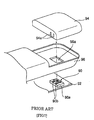
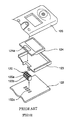
- Fig. 6 is a perspective view which shows an electrical connection device which connects a circuit substrate and a subsidiary substrate by means of such conventional connectors.
- an electrical connection device 80 which connects a circuit substrate 82 and a subsidiary substrate 84 by means of conventional connectors comprises a female connector 80b which is mounted on the subsidiary substrate 84, and a male connector 80a which is mounted on the circuit substrate 82.
- the circuit substrate 82 on which the male connector 80a is mounted is accommodated and fixed in an electronic part case 36.
- electrical connection to the circuit substrate 82 can be effected by means of the female connector 80b even after the circuit substrate 82 has been housed in the electronic part case 86.
- Fig. 7 - Fig. 10 are perspective views which show structures in which conventional electrical connection devices using such resilient elements are employed for portable mobile telephones, Fig. 7 showing an electrical connection device which uses resilient elements in the form of connection terminals, Fig. 8 another electrical connection device which uses resilient elements in the form of connection terminals, Fig. 9 an electrical connection device which uses a resilient element constituted by a coil spring, and Fig. 10 an electrical connection device which uses a resilient element in which electrically conductive portions and resilient portions are stacked.
- a conventional electrical connection device 90 in which resilient elements in the form of connection terminals are used comprises connection terminals 90b, which have one end mounted (not shown in the drawing) on a circuit substrate 92 and whose other ends are urged in the vertical direction, and a trunk portion 90a which holds these connection terminals 90b.
- This electrical connection device 90 is mounted on the circuit substrate 92, and is so installed that, when the circuit substrate 92 is fitted in a case 96 of a portable mobile telephone, the connection terminals 90b project from an opening portion 96a which is provided in the case 96. Therefore, electrical connection between the connection terminals 94a of a battery pack 94 and the connection terminals 90b of the circuit substrate 90 can easily be established by fitting the battery pack 94 on the case 96.
- an electrical connection device 100 which, as shown in Fig. 8, comprises a holder 100a which is fitted on a circuit substrate 102, and connection terminals 100c which are supported by the holder 100a.
- the holder 100a is formed to the general shape of an open box for the purpose of fitting it on the circuit substrate 102, and a projecting circular rib 100b is integrally formed on the upper surface of this generally open-box shape. Further, a portion of the rib 100b of the holder 100 is cut out, and the connection terminals 100c, which extend to the circuit substrate 102 via this cut-out portion, are fitted on.
- connection terminals 100c are soldered at one end to a set pattern of the circuit substrate 102, and they are so installed that their other ends are located at the interior of the rib 100b and are bent to a set angle and urged in the vertical direction. Therefore, when a microphone 104 is press-fitted into the rib 100b of the holder 100a, it is fixed, and, at the same time, its terminal portions 104a are electrically connected by coming into contact with the connection terminals 100c. Thus, the microphone 104 can easily be fitted on and electrically connected to the circuit substrate 102 even after the circuit substrate 102 has been fitted in a case (not shown) of a portable mobile telephone.
- a conventional electrical connection device 110 which uses a resilient element constituted by a spring, and in which, as shown in Fig. 9, there is provided a hollow holder 110a which has a generally cylindrical shape and in whose interior a coil spring 110b is inserted, and there is provision of an upper terminal 110c and a lower terminal 110d, which are respectively urged by opposite ends of this coil spring 110b.
- This electrical connection device 110 using a spring is so arranged that, when a circuit substrate and a subsidiary substrate such as shown in Fig. 6 are to be electrically connected, electrical connection can easily be established by an action in which, as illustrated in Fig.
- the terminal portions 112a and 114a of a circuit substrate 112 and a subsidiary substrate 114 are respectively brought into contact with the upper terminal 110c and lower terminal 110d at opposite ends of the electrical connection device 110 and pressed.
- electrical connection can be effected more easily with the electrical connection device 110 shown in Fig. 9 than it can with the electrical connection device using the connectors shown in Fig. 5.
- an electrical connection device 120 in which, as shown in Fig. 10, use is made of a resilient element in which plural electrically conductive portions 120a and resilient portions 120b are alternately overlaid and stacked.
- This electrical connection device 120 is supported by an LCD holder 123 of an LCD 124 which is fitted to a portable mobile telephone case 126, and it is installed in a manner such chat it contacts the terminal portion 124a of the LCD 124.
- the LCD holder 123 on which the LCD 124 and terminal portion 124a are mounted is fitted to the portable mobile telephone case 126, and, as the result of the further mounting of a circuit substrate 122, the electrical connection device 120 is pressed between the LCD 124 and the circuit substrate 122 and electrical connection can be established.
- the shape is complex, and the electrical connection device shown in Fig. 10 in particular has a structure in which plural layers are stacked, with the consequent drawback that the manufacturing cost becomes extremely high.
- the present invention has as its object to resolve the above problems and to provide a low-cost electrical connection device and an electronic instrument using this device with which a low profile for the electronic part main body is achieved, and the phenomenon on chattering is prevented.
- the insulation element here is formed from soft resin, contacts the 1st and 2nd electronic parts and absorbs vibration.
- one out of the 1st and 2nd electronic parts is a circuit substrate and the other is an electronic part.
- the holding member which holds the insulation element is provided extending from a holder which holds the other electronic part.
- plural conductors are passed through and held by the insulation element and are disposed either in zigzag form or in a straight line relative to the insulation element.
- the electronic instrument using the electrical connection device comprises an electrical connection device which is constituted by a conductor which has a coil shape and possesses resilience being passed through and held by an insulation element and is installed as the result of the insulation element being held by a set holding member, a 1st electronic part which contacts and presses a terminal portion at one end of the conductor of this electrical connection device and a 2nd electronic part which contacts and presses a terminal portion at the other end of the conductor of the electrical connection device.
- the electronic instrument here is a mobile communications terminal
- the insulation element is formed from soft resin, contacts the 1st and 2nd electronic parts and absorbs vibration.
- one out of the 1st and 2nd electronic parts is a circuit substrate and the other is an electronic part.
- the holding member which holds the insulation element is provided extending from a holder which holds the other electronic part, and plural conductors are passed through and held by the insulation element.
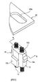
- Fig. 1 is a perspective view which shows a form of implementation in which the electrical connection device according to the invention is used for a portable mobile telephone.
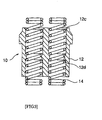
- Fig. 2 is an enlarged view showing details of the portion A indicated in Fig. 1.
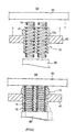
- Fig. 3 is a cross-sectional view which shows the cross section along the line B-B indicated in Fig. 2.
- Fig. 4 shows cross-sectional views in illustration of actions at the time when the electrical connection device shown in Fig. 1 is mounted in the case of a portable mobile telephone, Fig. 4(a) showing the state before mounting, and Fig. 4(b) the mounted state.
- the electrical connection device 10 is provided in a manner such that it can be press-fitted in a holding section 40a which is opened in a set surface which extends from an LCD holder 40.
- the LCD holder 40 which carries the electrical connection device 10 and an LCD 42, is fitted and fixed to a set surface of a circuit substrate 30.
- the LCD holder is fitted to the circuit substrate 30 in a manner such that a pair of coil springs 14 which pass through and are held by the internal portion of the electrical connection device 10 come into contact with terminal portions 30a which are formed on the surface of the circuit substrate 30.
- the circuit substrate 30 to which the LCD holder 40 and electrical connection device 10 have been fitted is mounted in the case 50 of a portable mobile telephone.
- the case 50 here has mounted therein a speaker 20 which has terminal portions 20a projecting towards the direction from which the circuit substrate 30 is mounted.
- the electrical connection device 10 brings the other ends of the coil springs 14 which pass through and are held by the internal portion into contact with the terminal portions 20a of the speaker 20, and the coil springs 14 are pressed from opposite ends.
- the electrical connection device 10 according to the invention is so provided that, as the result of a set electronic part being installed in the case of a portable mobile telephone, electrical connection between the electronic part and a circuit substrate is easily established.
- the electrical connection device 10 according to the invention is constituted by an insulation element 12, which is made of soft resin, and the pair of coil springs 14, which pass through and are held by the internal portion of this insulation element 12.
- the soft resin constituting the insulation element 12 here is constituted by, eg, Mitsubishi Chemical SJ4400B-N RABALON 45° material.
- the coil springs 14 which pass through and are held by the internal portion of the insulation element 12 are formed from, eg, SWP-B (piano wire) ⁇ 0.18 mm material and are given Ni or Au plating treatment.
- the insulation element 12 is formed by plastic injection moulding technique, and, as shown in Fig. 2, it has a generally cylindrical shape, and retention portions 12a, which project perpendicularly from opposite side surfaces, and a retention portion 12b, which, further, projects in a box shape in the direction which is at right angles to the directions in which the retention portions 12a project, are integrally formed. Further, cylindrical through-holes 12c which pass through from the top portion to the bottom portion are formed in two places in the insulation element 12. On the inner walls of these through-holes 12c, there are formed projections 12d, which project in the approximately midway portions of the through-holes 12c, as shown in Fig. 3.
- These projections 12d are provided in order to engage the coil springs 14, which are inserted in the through-holes 12c of the insulation element 12, and thereby prevent detachment of the coil springs 14 from the insulation element 12, Further, the coil springs 14 do not come out from the insulation element 12 easily, since, when they have been inserted in the through-holes 12, friction is produced through the contact of the outer peripheries of the coil springs 14 and the inner walls.
- the electrical connection device 10 is press-fitted in the holding section 40a of the LCD holder 40 (see Fig. 2).
- This electrical connection device 10 can easily be inserted into the holding section 40a, since, as noted above, the insulation element 12 and coil springs 14 possess flexibility.
- the retention portions 12a are allowed to pass through by the holding section 40a of the LCD holder 40, and the device is inserted until the peripheral edge portion of the holding section 40a is contacted by the retention portion 12b shown in Fig. 2.
- the retention portions 12a and the retention portion 12b are retained by the holding section 40a [sic], and the insulation element 12 is mounted on the LCD holder 40.
- the phenomenon of chattering of the coil springs 14 contacting the terminal portions 30a of the circuit substrate 30 and the terminal portions 20a of the speaker 20 can be prevented, since, if impact such as that of vibration, etc. is imposed from the exterior, it is absorbed by the insulation element 12.
- FIG. 5 shows perspective views in illustration of other forms of implementation of the electrical connection device according to the invention, Fig. 5(a) showing an electrical connection device 60 in which plural coil springs are disposed in a straight line, and Fig. 6(b) an electrical connection device 70 in which plural coil springs are disposed in zigzag form.
- the electrical connection device according to the invention is used for a portable mobile telephone
- the device may also be employed for electronic instruments such as mobile communications terminals and remote units (remote computing), etc.
- the electrical connection device according to the invention is used for speaker connection portions, there is no restriction to this, but the device can also be employed for electronic parts such as, eg, subsidiary substrates, power supplies, display units and switches, etc.
- the structure is one in which the terminal portions of a 1st electronic part and a 2nd electronic part are electrically connected by conductors which are in coil form and possess resilience, and these conductors are brought into contact with the 1st electronic part and 2nd electronic part while held by an insulation element made of soft resin, even if the main body of an electronic instrument is subjected to impact such as that of vibration, etc. from, the exterior, the impact is absorbed by the insulation element, and it is therefore possible to prevent the phenomenon of chattering of electrical connection portions.
- the electrical connection device since the structure is a simple one in which conductors which are in coil form and possess resilience are fitted in an insulation element made of soft resin, the shape can easily be made compact and it is possible to achieve lowering of the profile of an electronic instrument main body.
- the electrical connection device according to the invention possesses a simple structure as described above, a great reduction of manufacturing costs is possible, and a low-cost electrical connection device which is ideal for electrical connections can be produced.
Landscapes
- Coupling Device And Connection With Printed Circuit (AREA)
- Telephone Set Structure (AREA)
- Mounting Components In General For Electric Apparatus (AREA)
Applications Claiming Priority (2)
| Application Number | Priority Date | Filing Date | Title |
|---|---|---|---|
| JP30310498 | 1998-10-23 | ||
| JP10303104A JP2000133338A (ja) | 1998-10-23 | 1998-10-23 | 電気的接続装置及びそれを用いた電子機器 |
Publications (2)
| Publication Number | Publication Date |
|---|---|
| EP0996197A2 true EP0996197A2 (de) | 2000-04-26 |
| EP0996197A3 EP0996197A3 (de) | 2003-01-29 |
Family
ID=17916945
Family Applications (1)
| Application Number | Title | Priority Date | Filing Date |
|---|---|---|---|
| EP99308343A Withdrawn EP0996197A3 (de) | 1998-10-23 | 1999-10-22 | Elektrische Verbindungsvorrichtung und elektronisches Instrument unter deren Verwendung |
Country Status (3)
| Country | Link |
|---|---|
| US (1) | US6299457B1 (de) |
| EP (1) | EP0996197A3 (de) |
| JP (1) | JP2000133338A (de) |
Cited By (2)
| Publication number | Priority date | Publication date | Assignee | Title |
|---|---|---|---|---|
| WO2002043189A1 (de) * | 2000-11-23 | 2002-05-30 | Moeller Gmbh | Elektrische anordnung |
| EP1830620A1 (de) * | 2006-03-03 | 2007-09-05 | Lih Duo International Co., Ltd. | Elastomerischer Verbinder |
Families Citing this family (8)
| Publication number | Priority date | Publication date | Assignee | Title |
|---|---|---|---|---|
| JP3804925B2 (ja) * | 2001-10-23 | 2006-08-02 | パイオニア株式会社 | スピーカのコネクタ |
| KR100473788B1 (ko) * | 2002-07-15 | 2005-03-10 | 주식회사 씨에스티 | 마이크로폰용 커넥터 |
| US6846184B2 (en) * | 2003-01-24 | 2005-01-25 | High Connection Density Inc. | Low inductance electrical contacts and LGA connector system |
| CA2425077C (en) * | 2003-04-10 | 2005-10-18 | Research In Motion Limited | Electrical connector assembly |
| US7258550B2 (en) * | 2003-04-10 | 2007-08-21 | Research In Motion Limited | Electrical connector assembly |
| US6783405B1 (en) * | 2003-11-28 | 2004-08-31 | Chuan Yi Precision Industry Co., Ltd. | Terminal for electric connector for communication apparatus |
| KR100714599B1 (ko) * | 2004-12-21 | 2007-05-07 | 삼성전기주식회사 | 무선통신 단말기의 내장형 안테나 조립체 |
| CN101169455B (zh) * | 2007-10-09 | 2010-10-06 | 番禺得意精密电子工业有限公司 | 探针 |
Family Cites Families (5)
| Publication number | Priority date | Publication date | Assignee | Title |
|---|---|---|---|---|
| FR2614494B1 (fr) * | 1987-04-22 | 1989-07-07 | Power Compact | Procede d'assemblage de circuits de puissance et de circuits de commande sur plusieurs niveaux sur un meme module et module ainsi obtenu |
| US5297967A (en) * | 1992-10-13 | 1994-03-29 | International Business Machines Corporation | Electrical interconnector with helical contacting portion and assembly using same |
| US5504940A (en) * | 1992-11-13 | 1996-04-02 | Motorola, Inc. | Shock isolation system having integral electrical interconnects |
| JPH07161416A (ja) * | 1993-12-02 | 1995-06-23 | Excel Denshi:Kk | 基板用コネクタ |
| US5602490A (en) * | 1995-03-14 | 1997-02-11 | Genrad, Inc. | Connector for automatic test equipment |
-
1998
- 1998-10-23 JP JP10303104A patent/JP2000133338A/ja not_active Withdrawn
-
1999
- 1999-10-22 EP EP99308343A patent/EP0996197A3/de not_active Withdrawn
- 1999-10-22 US US09/422,184 patent/US6299457B1/en not_active Expired - Fee Related
Cited By (2)
| Publication number | Priority date | Publication date | Assignee | Title |
|---|---|---|---|---|
| WO2002043189A1 (de) * | 2000-11-23 | 2002-05-30 | Moeller Gmbh | Elektrische anordnung |
| EP1830620A1 (de) * | 2006-03-03 | 2007-09-05 | Lih Duo International Co., Ltd. | Elastomerischer Verbinder |
Also Published As
| Publication number | Publication date |
|---|---|
| JP2000133338A (ja) | 2000-05-12 |
| US6299457B1 (en) | 2001-10-09 |
| EP0996197A3 (de) | 2003-01-29 |
Similar Documents
| Publication | Publication Date | Title |
|---|---|---|
| US6796849B2 (en) | Electrical connection device | |
| JPH11273806A (ja) | 電気コネクタ | |
| JP3035814B2 (ja) | 表面係合式電気コネクタ | |
| JPH0676894A (ja) | コネクタ | |
| WO2004023604A1 (ja) | コネクタ | |
| US20130295796A1 (en) | Multiple plug connector unit | |
| CN1095226C (zh) | 便携式电话连接系统 | |
| US20110263158A1 (en) | Electrical connector | |
| JPS6035791B2 (ja) | 電気接続端子 | |
| US6299457B1 (en) | Electrical connection device and electronic instrument using it | |
| JPWO2003015221A1 (ja) | コネクタ | |
| JP4613799B2 (ja) | 基板接続用コネクタ組立体 | |
| JP2003143679A (ja) | コンデンサマイクロホン及びこれを用いた携帯電話機器 | |
| JP2002246119A (ja) | 電気コネクタ | |
| US7118393B1 (en) | Bonded elastomeric connector | |
| JPH1141682A (ja) | マイク取付装置及び取付方法 | |
| CN101473496B (zh) | 同轴电缆用连接器 | |
| JP3556592B2 (ja) | 振動部品用コネクタ | |
| US6319054B1 (en) | Electrical connector | |
| US11462851B2 (en) | Machine case and cable connector assembly | |
| KR20040023700A (ko) | 힌지용 커넥터 및 이 커넥터에 접속되는 회로 기판 | |
| JP3035544B1 (ja) | コネクタタ―ミナル | |
| JP3085988B2 (ja) | 電気的なコネクタ | |
| JP4308941B2 (ja) | 端子付きレシーバおよび端子付きレシーバを用いた移動体通信装置 | |
| US20240186730A1 (en) | Electrical Connector, Connecting Body Between a Circuit Board and Electrical Connector |
Legal Events
| Date | Code | Title | Description |
|---|---|---|---|
| PUAI | Public reference made under article 153(3) epc to a published international application that has entered the european phase |
Free format text: ORIGINAL CODE: 0009012 |
|
| AK | Designated contracting states |
Kind code of ref document: A2 Designated state(s): AT BE CH CY DE DK ES FI FR GB GR IE IT LI LU MC NL PT SE |
|
| AX | Request for extension of the european patent |
Free format text: AL;LT;LV;MK;RO;SI |
|
| RAP1 | Party data changed (applicant data changed or rights of an application transferred) |
Owner name: NOKIA CORPORATION |
|
| PUAL | Search report despatched |
Free format text: ORIGINAL CODE: 0009013 |
|
| AK | Designated contracting states |
Designated state(s): AT BE CH CY DE DK ES FI FR GB GR IE IT LI LU MC NL PT SE |
|
| AX | Request for extension of the european patent |
Extension state: AL LT LV MK RO SI |
|
| 17P | Request for examination filed |
Effective date: 20030310 |
|
| 17Q | First examination report despatched |
Effective date: 20030701 |
|
| AKX | Designation fees paid |
Designated state(s): DE ES FR GB |
|
| STAA | Information on the status of an ep patent application or granted ep patent |
Free format text: STATUS: THE APPLICATION IS DEEMED TO BE WITHDRAWN |
|
| 18D | Application deemed to be withdrawn |
Effective date: 20040113 |