EP0997712A2 - Kapazitive Sensoranordnung in einem flüssigen Medium sowie Herstellungsverfahren - Google Patents
Kapazitive Sensoranordnung in einem flüssigen Medium sowie Herstellungsverfahren Download PDFInfo
- Publication number
- EP0997712A2 EP0997712A2 EP99121294A EP99121294A EP0997712A2 EP 0997712 A2 EP0997712 A2 EP 0997712A2 EP 99121294 A EP99121294 A EP 99121294A EP 99121294 A EP99121294 A EP 99121294A EP 0997712 A2 EP0997712 A2 EP 0997712A2
- Authority
- EP
- European Patent Office
- Prior art keywords
- carrier
- plates
- carrier plates
- capacitor
- cavity
- Prior art date
- Legal status (The legal status is an assumption and is not a legal conclusion. Google has not performed a legal analysis and makes no representation as to the accuracy of the status listed.)
- Granted
Links
Images


Classifications
-
- G—PHYSICS
- G01—MEASURING; TESTING
- G01F—MEASURING VOLUME, VOLUME FLOW, MASS FLOW OR LIQUID LEVEL; METERING BY VOLUME
- G01F23/00—Indicating or measuring liquid level or level of fluent solid material, e.g. indicating in terms of volume or indicating by means of an alarm
- G01F23/22—Indicating or measuring liquid level or level of fluent solid material, e.g. indicating in terms of volume or indicating by means of an alarm by measuring physical variables, other than linear dimensions, pressure or weight, dependent on the level to be measured, e.g. by difference of heat transfer of steam or water
- G01F23/26—Indicating or measuring liquid level or level of fluent solid material, e.g. indicating in terms of volume or indicating by means of an alarm by measuring physical variables, other than linear dimensions, pressure or weight, dependent on the level to be measured, e.g. by difference of heat transfer of steam or water by measuring variations of capacity or inductance of capacitors or inductors arising from the presence of liquid or fluent solid material in the electric or electromagnetic fields
- G01F23/263—Indicating or measuring liquid level or level of fluent solid material, e.g. indicating in terms of volume or indicating by means of an alarm by measuring physical variables, other than linear dimensions, pressure or weight, dependent on the level to be measured, e.g. by difference of heat transfer of steam or water by measuring variations of capacity or inductance of capacitors or inductors arising from the presence of liquid or fluent solid material in the electric or electromagnetic fields by measuring variations in capacitance of capacitors
- G01F23/268—Indicating or measuring liquid level or level of fluent solid material, e.g. indicating in terms of volume or indicating by means of an alarm by measuring physical variables, other than linear dimensions, pressure or weight, dependent on the level to be measured, e.g. by difference of heat transfer of steam or water by measuring variations of capacity or inductance of capacitors or inductors arising from the presence of liquid or fluent solid material in the electric or electromagnetic fields by measuring variations in capacitance of capacitors mounting arrangements of probes
-
- G—PHYSICS
- G01—MEASURING; TESTING
- G01F—MEASURING VOLUME, VOLUME FLOW, MASS FLOW OR LIQUID LEVEL; METERING BY VOLUME
- G01F23/00—Indicating or measuring liquid level or level of fluent solid material, e.g. indicating in terms of volume or indicating by means of an alarm
- G01F23/22—Indicating or measuring liquid level or level of fluent solid material, e.g. indicating in terms of volume or indicating by means of an alarm by measuring physical variables, other than linear dimensions, pressure or weight, dependent on the level to be measured, e.g. by difference of heat transfer of steam or water
- G01F23/26—Indicating or measuring liquid level or level of fluent solid material, e.g. indicating in terms of volume or indicating by means of an alarm by measuring physical variables, other than linear dimensions, pressure or weight, dependent on the level to be measured, e.g. by difference of heat transfer of steam or water by measuring variations of capacity or inductance of capacitors or inductors arising from the presence of liquid or fluent solid material in the electric or electromagnetic fields
- G01F23/263—Indicating or measuring liquid level or level of fluent solid material, e.g. indicating in terms of volume or indicating by means of an alarm by measuring physical variables, other than linear dimensions, pressure or weight, dependent on the level to be measured, e.g. by difference of heat transfer of steam or water by measuring variations of capacity or inductance of capacitors or inductors arising from the presence of liquid or fluent solid material in the electric or electromagnetic fields by measuring variations in capacitance of capacitors
Definitions
- the invention relates to a capacitive sensor arrangement in a liquid or gaseous medium, which acts as a dielectric on the capacitive sensor arrangement acts, as well as a method for producing this sensor arrangement.
- Such Sensor arrangements are used in particular for level measurement, whereby basically other parameters from the dielectric properties of the Medium can be derived.
- the carrier plates are structured from printed circuit board material by etching and have in part a carrier plate a plurality of spaced-apart capacitor layers, For example, a main electrode for level measurement and a dielectric measuring electrode to measure the changing dielectric, and protective assignments for electrical shielding, these differing Elements on the carrier plates by conductor tracks with one each Connection area are connected.
- the individual capacitor layers on the carrier plates as well as, if applicable, the further elements are from these connection areas on the individual carrier plates with a spatial one Construction not shown in detail, obviously arranged separately electronic Measuring device connected.
- the required electrical connections for the individual carrier plates are prone to failure and expensive.
- the measuring accuracy of the arrangement is also strongly dependent on the stability and thus the number and spacing of the rivets depends on each other. So through the Rivets cannot always be ensured that the carrier plates are not but bend and so a non-constant distance and thus measurement deviations cause.
- the object of the invention is to present a capacitive sensor arrangement which on the one hand it is easy to manufacture and on the other hand it guarantees an accurate measurement, and to specify a corresponding method for the production.
- the multi-level circuit board technology known per se can be used very advantageously for capacitive sensor arrangements can, each as a spacer between two carrier plates Intermediate plate with a cavity is provided. This cavity is formed through a central recess in the intermediate plate that in the area is arranged in which the adjacent carrier plates, the capacitor coatings exhibit. There remains an edge area that the adjacent carrier plates holds at the desired distance, the distance by the thickness of the Intermediate plate is exactly determined.
- there are inflows and outflows of the medium in and out of the cavity or for pressure equalization further cutouts laterally in the edge area of the intermediate plate or directly into the Carrier plates provided.
- the carrier and intermediate plates are metallized Vias electrically connected to each other.
- the sensor arrangement can be assembled as a hollow multilayer, i.e. one Multi-level PCB arrangement with cavities for the medium to be measured to be discribed. The edge areas of the intermediate plate can clearly ensure better stability and thus measurement accuracy.
- the evaluation circuit can be on the outside an outer support plate can be integrated, so that a complicated and electrical connection prone to interference, for example completely avoided by bonding wires can be.
- the figures show particularly preferred exemplary embodiments with three in parallel mutually arranged carrier plates 1, 3 and 5 between each one Intermediate plate 2 and 4 is arranged and thus an arrangement of 5 levels form.
- sensor arrangements with only two plates are, of course possible.
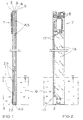
- Figure 1 shows a side view of a capacitive sensor arrangement.
- the carrier plates 1, 3 and 5 to the bottom of the Protrude container, while the intermediate plates between them as spacers 2 and 4 have lower cutouts 2.2 and 4.2 through which the medium 6 into the cavities (2.1, 4.1) can penetrate.
- These cavities are shown in later figures, in particular 3 and 4 shown in more detail and explained accordingly.
- Fig. 1 st laterally arranged recesses 2.3 and 4.3 in the remaining edge region of the Intermediate plates 2 and 4 enable the medium 6 to flow in and out or the pressure equalization, so that the fill level of the medium 6 within the cavities (2.1.4.1) to the fill level outside the sensor arrangement.
- the distance between the support plates 1, 3 and 5 is determined by the thickness of the Intermediate plates 2 and 4 determined and is preferably chosen so that the in Cavity-acting capillary forces for the accuracy of the level measurement are negligible.
- the outside is 1.0 of the first carrier plate 1 configured with an evaluation circuit 7, which is shown even more clearly in FIG. 2 is shown sketchily in the front view.
- an evaluation circuit 7 which is shown even more clearly in FIG. 2 is shown sketchily in the front view.
- another sensor 9 provided, for example, the temperature or the chemical composition or quality of the medium 6 detected.
- the medium 6 can be liquid or be gaseous.
- an oil level sensor is shown as it is intended for motor vehicles.
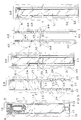
- FIG. 3 now shows the front sides 1.0.2.0.3.0.4.0.5.0 of the 5 individual levels, ie the carrier plates 1, 3 and 5 and the intermediate plates 2 and 4 in an exploded view laterally offset from each other.
- the carrier plates 1, 3 and 5 are with each other through the intermediate plates 2 and 4 through metallized Bores, so-called vias 8 connected to each other, wherein a part of each according to the circuit to be implemented Vias 8 via interconnects 1.7,3.4,5.4 with the capacitor coatings 3.1.5.1, shielding metal coverings 1.3.2.7.3.2 or components 7,9 are connected, as will be explained in more detail with reference to FIG. 6.
- the front corresponds to the first support plate 1 and thus one of the two outer sides of the sensor arrangement of the illustration in FIG. 2 and shows the Evaluation circuit 7 with interconnects 1.7 and components and one Metal covering 1.3 for shielding against electromagnetic fields. Also are SMD - contact points for the sensor 9 to be recognized.
- the intermediate plate 2 underneath when installed is offset shown, which borders in the lower area by an edge area 2.4 has middle recess 2.1, which forms a cavity in the through the lower Recess 2.2 and the lateral recesses 2.3 flow in and out of the medium 6, especially the level corresponding to the level outside the Can adjust cavity.
- the individual sections of the marginal area 2.4 Intermediate plate 2 serve as additional stabilization between the cutouts 2.3 and are preferably larger than the recesses 2.3.
- the marginal areas 2.4 are connected to each other before cutting free by struts 2.5, as shown in Fig. 5 becomes even clearer.
- the size of the middle recess 2.1 is adapted to the adjacent capacitor coatings 1.1 of the first and 3.1 of the second, middle carrier plate 3.
- the intermediate plate 2 can also be used in the upper area a metal covering 2.7 can be provided as a shield.
- the one remaining on the side Edge area 2.6 is generally not metallized, since there the adhesive for Connecting the carrier plates 1,3,5 with the intermediate plates 2,4 is applied.
- the second and middle carrier plate 3 represents the third level of the sensor arrangement and is again shown offset to the front view.
- the second Carrier plate 3 has a capacitor covering 3.1 in the lower region, which of is surrounded by a metallic edge 3.3, which, however, is covered by the capacitor covering 3.1 is spaced or isolated.
- the metallic edge 3.3 is used for shielding. He is interrupted, for example, for interconnects 3.4 to the individual capacitor coatings.
- the upper area of the front can also be used for shielding purposes
- the interconnect 3.4 between a metallic bore 8 for Capacitor coating 3.1 can be seen.
- the second intermediate plate 4 in FIG. 3 now has one in this exemplary embodiment Middle cutout 4.1 extending over the entire length of the sensor arrangement corresponding to the capacitor coating 5.1 on the third carrier plate 5. Laterally are the edge areas 4.2 of the intermediate plate 4 for keeping the distance constant between the two carrier plates 3 and 5 or those arranged thereon Capacitor coverings 3.6 (3.6 is on the back of the second carrier plate 3, shown in Figure 4) and 5.1 arranged.
- the intermediate plate 4 has lower Recesses 4.2 and 4.3 lateral recesses for the medium 6, with a partial filling of the resulting cavity with the medium the top Lateral cutouts 4.3 allow volume or pressure equalization.
- the front of the third plate 5 is also shown laterally offset, which has the capacitor covering 5.1 in the middle over the entire length of the connected via an interconnect 5.4 to one of the metallized bores 8 and from a metallic edge 5.3 is shielded from other field influences.
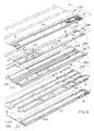
- FIG. 4 shows the rear sides 1.r, 2.r, 3.r, 4.r, 5.r of the 5 levels, the Capacitor coating 1.1 on the back 1.r of the first carrier plate 1 symmetrically to the capacitor coating 3.1 on the second carrier plate 3 and with this one forms the first capacitor arrangement, for example if a minimum fill level is maintained is always completely filled with the medium 6 and therefore for determining the relative dielectric constant of the medium 6 is used.
- the intermediate plates 2 and 4 are preferably identical on the front and back. Again they are Capacitor arrangement 1.1 orbits 1.4 and additionally on the free Surfaces of metal 1.2 provided for shielding.
- the rear side 3.r of the second plate 3 has, analogously to the capacitor covering 5.1 the front of the third plate 5 on a capacitor 3.6.
- the dielectric constant determined from the first capacitor arrangement is taken as a basis.
- insert strips 13 are indicated in FIG Intermediate plates 2 and 4 with the adjacent carrier plates 1,3,5 in the middle Recesses 2.1.4.1 are inserted and prevents from sticking through the pressure, the carrier plates 1,3,5 are bent. Below is the Insert strips 13 removed again through the lower cutouts 2.2., 4.2.
- the Back side 5.r has an outward-facing surface Shielding covering 5.2.
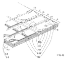
- FIGS. 5 and 10 illustrate the parallel production of several of these sensor arrangements at the same time side by side in multi-level circuit board technology by on the panels 100, 300 and 500 each made of carrier plate material spaced apart from one another several identical arrangements are generated. So the board 100 points several first plates 1 side by side and the plate 200 several of the Intermediate plates 2, the individual segments with struts 2.5 to one another are connected. This continues accordingly on the panels 300 to 500. All these panels 100 to 500 are glued to one another aligned and then cut out the individual sensor arrays, the struts 1.5,2.5,3.5,4.55.5 between the individual segments of the intermediate and carrier plates 1,2,3,4,5 are separated.
- Figure 10 illustrates this joint production again, with the Subdivision of the plates 100,200,300,400,500 of the carrier and intermediate plates into Segments A, B, C, ... and their connection by the struts 1.5.2.5.3.5.4.5.5.5 is sketchily indicated.
- the plated-through holes 8 are also visualized.
- the lower inflow openings 4.2 lying next to one another are identical and 2.2 of the cavities 2.1 and 4.1.
- the cavity 4.1 through lateral openings 4.3 is balanced, is the other for the cavity 2.1 Alternatively shown with an opening 1.6 in the carrier plate 1, which is shown in FIGS and 9 is shown in more detail.
- Figure 6 and the enlarged section 6a show a section through the Sensor arrangement consisting of the three carrier plates 1, 3 and 5 with the Intermediate plates 2 and 4.
- metal coverings 1.3 and 5.2 are provided for shielding.
- the plates additionally have the metallic edges 1.4, 3.3 and 5.3, which are also connected to ground together.
- metallized hole 8 between the five levels 1 to 5 shown that has this ground connection and with these edges 1.3, 3.3 and 5.3 and the metal coverings 1.5 and 5.5 correspondingly formed from interconnects Contact zones is connected.
- the introduction of the vias 8 and their connection on the individual carrier plates 1,3,5 is in itself already from the Multi-level circuit board technology known.
- FIG. 6 and 6a are those formed by the intermediate plates 2 and 4 Cavities for the medium and those arranged on both sides of it Capacitor pads 1.1 and 3.1 for the first capacitor arrangement and 3.6 and 5.1 for the second capacitor arrangement.
- Figure 6 also shows how the sensor arrangement is arranged in a shielding tube 11, which also with its openings 12 for the medium is shown in Figure 7.
- the evaluation circuit 7 is protected by a potting compound 10.
- copper-clad printed circuit boards as carrier plates 1,3,5 can be replaced by a simple etching process the capacitor coatings 1.1.3.1.3.6.5.1, metal coatings 1.2.1.3, 3.2.5.2 and metallic tracks 1.4.3.3.5.3 of the shields and the interconnects 1.7.3.4.5.4 are structured.
- the multi-level circuit board technology already suitable adhesives, insulation coatings etc. as well as the Technique for metallizing the holes 8 is known.
- FIG. 8 shows the alternative embodiment in a further exemplary embodiment of the openings 1.6 and 5.6 in the carrier plates 1 and 5 for input and Outflow of the medium 6 into or out of the respective cavity 2.1 and 4.1 or for pressure equalization.
- This flow or the pressure equalization is illustrated also with a vertical cut through the carrier and intermediate plates 1-5 in Figure 9, where through the openings 1.6 and 2.2, the cavity 2.1 in the first Intermediate plate is flowed through, while the medium 6 in through the opening 4.2 the cavity 4.1 in the second intermediate plate 4 up to that in the outer container the present fill level rises and through the opening 5.6 in the lower carrier plate 5 pressure equalization takes place.
Landscapes
- Physics & Mathematics (AREA)
- Engineering & Computer Science (AREA)
- Power Engineering (AREA)
- Electromagnetism (AREA)
- Thermal Sciences (AREA)
- Fluid Mechanics (AREA)
- General Physics & Mathematics (AREA)
- Measurement Of Levels Of Liquids Or Fluent Solid Materials (AREA)
- Investigating Or Analyzing Materials By The Use Of Electric Means (AREA)
Abstract
Description
- Figur 1
- Seitenansicht einer kapazitiven Sensoranordnung aus zwei parallelen Kondensatoranordnungen in einem flüssigen oder gasförmigen Medium
- Figur 2
- Vorderansicht der kapazitiven Sensoranordnung gemäß Figur 1
- Figur 3
- Explosionsdarstellung der Sensoranordnung - die Vorderseiten der einzelnen Ebenen
- Figur 4
- Explosionsdarstellung der Sensoranordnung - die Rückseiten der einzelnen Ebenen
- Figur 5
- Darstellung des Herstellungsprozesses mit dem Freischneiden der einzelnen Sensoranordnungen, insbesondere der Zwischenplattenaus der Mehrebenenanordnung
- Figur 6
- Schnitt durch die Sensoranordnung
- Figur 7
- Sensoranordnung in einem Abschirmrohr mit Öffnungen zum Strömen des Mediums
- Figur 8
- Explosionsdarstellung einer weiteren Ausgestaltung mit Öffnungen in den äußeren Trägerplatten zum Ein- und Ausströmen des Mediums
- Figur 9
- Schnitt durch die Sensoranordnung gemäß Figur 8
- Figur 10
- Verdeutlichung der Herstellung in Mehrebenen-Leiterplattentechnik mit Tafeln aus Träger- und Zwischenplattenmaterial, die in identische Segmente unterteilt und über Streben verbunden gleichzeitig strukturiert und nachfolgend entlang der Streben freigeschnitten werden
- 1
- erste Trägerplatte, 1.0 - Vorderseite, 1 .r = Rückseite
- 1.1
- Kondensatorbelag (rückseitig)
- 1.2
- abschirmender Metallbelag
- 1.3
- abschirmender Metallbelag
- 1.4
- umlaufende Abschirmungsbahn
- 1.5
- Strebe zwischen den einzelnen Trägerplattensegmenten der Tafel
- 1.6
- Löcher als Strömungsöffnungen für das Medium 6
- 1.7
- Leitbahnen zwischen Sensor, Auswerteschaltung und Durchkontaktierungen
- 2
- Zwischenplatte (2.Ebene), 2.0 = Vorderseite, 2.r = Rückseite
- 2.1
- mittlere, den Hohlraum bildende Aussparung
- 2.2
- untere Einströmöffnung
- 2.3
- seitliche Stömungsöffnung in der Zwischenplatte 2
- 2.4
- abstandhaltender Randbereich um den Hohlraum
- 2.5
- Verbindungsträger für die einzelnen Abstandshalterabschnitte
- 2.6
- Randzone mit Durchkontaktierungen
- 2.7
- Abschirmung
- 3
- mittlere Trägerplatte (3.Ebene), 3.0 = Vorderseite, 3.r = Rückseite
- 3.1
- vorderseitiger Kondensatorbelag
- 3.2
- Abschirmungsbelag
- 3.3
- Abschirmbahn
- 3.4
- Leitbahn zwischen 8 und 3.1
- 3.5
- Strebe zwischen den einzelnen Trägerplattensegmenten der Tafel
- 3.6
- rückseitiger Kondensatorbelag
- 4
- 2. Zwischenplatte (4.Ebene), 4.0 = Vorderseite, 4.r = Rückseite
- 4.1
- mittlere, den Hohlraum bildende Aussparung
- 4.2
- untere Einströmöffnung
- 4.3
- obere Stömungsöffnung
- 4.4
- abstandhatender Randbereich
- 4.5
- Trägerstrebe für einzelnen Segmente des Abstandhalters
- 5
- 3. Trägerplatte (5.Ebene), 5.0 = Vorderseite, 5.r = Rückseite
- 5.1
- Kondensatorbelag
- 5.2
- abschirmender Metallbelag
- 5.3
- Abschirmbahn
- 5.4
- Leitbahn zwischen Kondensatorbelag und Durchkontaktierung
- 5.5
- Strebe zwischen den einzelnen Trägerplattensegmenten der Tafel
- 5.6
- Löcher zum Ein- und Ausströmen des Mediums bzw. zum Druckausgleich
- 6
- Medium
- 7
- Auswerteschaltung
- 8
- Vias/Durchkontaktierungen
- 9
- Ölqualitätssensor oder Temperatursensor
- 10
- Vergußmasse zur Fixierung der Auswerteschaltung
- 11
- Abschirmrohr
- 12
- Strömungsöffnungen im Rohr für das Medium
- 13
- Teflon-Einlagestreifen
- 100
- Tafel aus Trägerplattenmaterial mit Segmenten A,B,C,... der ersten Trägerplatte 1
- 200
- Tafel aus Zwischenplattenmaterial mit Segmenten A,B,C,... der ersten Zwischenplatte 2
- 300
- Tafel aus Trägerplattenmaterial mit Segmenten A,B,C,... der mittleren Trägerplatte 3
- 400
- Tafel aus Zwischenplattenmaterial mit Segmenten A,B,C,... der ersten Zwischenplatte 2
- 500
- Tafel aus Trägerplattenmaterial mit Segmenten A,B,C,... der dritten Trägerplatte 5
Claims (14)
- Kapazitive Sensoranordnung in einem flüssigen oder gasförmigen Medium (6),a) bestehend aus wenigstens zwei in einem durch Abstandshaltemittel vorgegebenen Abstand parallel angeordneten Trägerplatten (1,3,5),b) wobei auf zueinander gerichteten Seiten zweier benachbarter Trägerplatten jeweils metallische Kondensatorbeläge (1.1/3.1 und 3.6/5.1) angeordnet sind, die durch Verschaltung einen Kondensator bilden, der vom Medium (6) zumindest teilweise gefüllt ist, dadurch gekennzeichnet, daßc) als Abstandshaltemittel zwischen zwei benachbarten Trägerplatten (1,3,5) jeweils eine Zwischenplatte (2,4) vorgesehen ist, deren äußere Abmessungen denen der Trägerplatten im wesentlichen entsprechen und die Zwischenplatten (2,4) im Bereich, in dem die benachbarten Trägerplatten (1,3,5) die Kondensatorbeläge (1.1/3.1 und 3.6/5.1) aufweisen, zur Erzeugung eines Hohlraums mit einer mittleren Aussparung (2.1,4.1) versehen ist undd) darüber hinaus in den Träger- und/oder Zwischenplatten (1,2,3,4,5) mehrere Aussparungen (1.6,2.2,2.3,4.2,4.3,5.6) zum Ein - und Ausströmen des Mediums (6) in und aus dem Hohlraum (2.1,4.1) vorgesehen sind.
- Sensoranordnung nach Anspruch 1, dadurch gekennzeichnet, daß in der Zwischenplatte (2,4) um den Hohlraum (2.1,4,.1) ein Randbereich (2.4,4.4) verbleibt, der durch die Aussparungen (2.2,2.3,4.2,4.3) zum Ein - und Ausströmen des Mediums (6) in und aus dem Hohlraum (2.1,4.1) unterbrochen ist, wobei die Ausdehnung der Aussparungen (2.2,2.3,4.2,4.3) im Randbereich (2.4,4.4) vorzugsweise kleiner ist als der durch diese Aussparungen verbleibende Randbereich der Zwischenplatte (2,4).
- Sensoranordnung nach Anspruch 1, dadurch gekennzeichnet, daß die Aussparungen (1.6,5.6) zum Ein - und Ausströmen des Mediums (6) in und aus dem Hohlraum (2.1,4.1) zumindest teilweise durch Löcher (1.6,5.6) in den Trägerplatten (1,5) ausgebildet sind.
- Sensoranordnung nach einem der vorangehenden Ansprüche, dadurch gekennzeichnet, daß durch die Trägerplatten (1,3,5) als auch durch die Zwischenplatten (2,4) hindurch metallisierte Durchkontaktierungen (8) vorgesehen sind, die auf einzelnen Seiten der Trägerplatten (1,3,5) über Leiterbahnen (3.4) zumindest teilweise mit Kondensatorbelägen (1.1/3.1 und 3.6/5.1) verbunden sind.
- Sensoranordnung nach Anspruch 4, dadurch gekennzeichnet, daßa1) bei genau zwei Trägerplatten auf zumindest einer dieser zwei beziehungsweisea2) bei drei und mehr Trägerplatten auf zumindest einer außen liegenden Trägerplatte (1)b) auf der von den anderen Trägerplatten (3,5) abgewandten Seite mit Sensoren, Leitbahnen und einer Auswerteschaltung (7) versehen ist, wobei die Auswerteschaltung (7) über die Leitbahnen (1.7,3.4,5.4) und Durchkontaktierungen (8) mit den Kondensatorbelägen (1.1/3.1 und 3.6/5.1) auf den einzelnen Trägerplatten (1,3,5) verbunden ist.
- Sensoranordnung nach einem der vorangehenden Ansprüche, dadurch gekennzeichnet, daß wenigstens drei Trägerplatten vorgesehen sind und die beidseitig zumindest einer mittleren Trägerplatte (3) angeordneten Kondensatorbeläge (3.1,3.6) beide auf ein gleiches Spannungspotential geschaltet sind.
- Sensoranordnung nach einem der vorangehenden Ansprüche, dadurch gekennzeichnet, daß die Trägerplatten (1,3,5) mit einer Abschirmung in Form einer den Kondensatorbelag (1.1,3.1,3.6,5.1) zumindest teilweise umlaufenden, von dem Kondensatorbelag jedoch getrennten metallischen Bahn (1.4,3.3,5.3) versehen ist, welche auf ein Bezugspotential geschaltet ist.
- Sensoranordnung nach Anspruch 6 und 7, dadurch gekennzeichnet, daß die beidseitig einer mittleren Trägerplatte (3) angeordneten Kondensatorbeläge (3.1,3.6) beide auf das Bezugspotential geschaltet sind.
- Sensoranordnung nach einem der vorangehenden Ansprüche, dadurch gekennzeichnet, daßa1) bei genau zwei Trägerplatten auf diesena2) bei drei und mehr Trägerplatten auf den außen liegenden Trägerplatten (1,5)b) auf den entgegengesetzt zu der/den anderen Trägerplatte(n) gerichteten Seiten mit jeweils einem Metallbelag (1.3, 5.2) versehen sind, welcher zur Abschirmung auf ein Bezugspotential geschaltet ist.
- Verfahren zur Herstellung einer Sensoranordnung nach einem der vorangehenden Ansprüche, dadurch gekennzeichnet, daß in Mehrebenen-Leiterplattentechnik:a) auf den Trägerplatten (1,3,5) durch Metallabscheidung und Ätzstrukturierung Kondensatorbeläge (1.1/3.1 und 3.6/5.1), Leitbahnen (1.7,3.4,5.4) und/oder zur Abschirmung dienende metallischen Bahnen (1.4,3.3,5.3) und Metallbeläge (1.3, 5.2) gemeinsam aufgebracht und strukturiert werden,b) die Träger- und Zwischenplatten zumindest örtlich untereinander durch Klebstoff mechanisch verbunden werden,c) durch die Trägerplatten (1,3,5) als auch die mit den Aussparungen versehenen Zwischenplatten (2,4) metallisierte Durchkontaktierungen (8) eingebracht werden, die mit den Kondensatorbelägen (1.1/3.1 und 3.6/5.1), Leitbahnen (1.7,3.4,5.4) und/oder zur Abschirmung dienenden metallischen Bahnen (1.3,3.3,5.3) und Metallbelägen (1.3, 5.2) zumindest teilweise elektrisch verbunden sind.
- Verfahren nach Anspruch 10, dadurch gekennzeichnet, daß eine Anzahl von Sensoranordnungen gleichzeitig hergestellt wird, indem :a) Tafeln (100,200,300,400,500) aus Träger- und Zwischenplattenmaterial in entsprechend der Anzahl von Sensoranordnungen viele Segmente (A,B,C,..) unterteilt werden, wobei die Segmente (A,B,C,..) voneinander beabstandet die Träger- und Zwischenplatten (1,2,3,4,5) bilden und die einzelnen Segmente am Rand eines jeden Segments über Streben (1.5,2.5,3.5,4.5,5.5) verbunden sind,b) auf einer jeden dieser Tafeln aus Trägerplattenmaterial (100,300,500) die Segmente (A,B,C,..) identisch mit Kondensatorbelägen (1.1,3.1,3.6,5.1), Leitbahn(en) (1.7,3.4,5.4) und/oder zur Abschirmung dienende metallischen Bahnen (1.4,3.3,5.3) und Metallbelägen (1.3, 5.2) strukturiert werden,c) aus der/den Tafel(n) aus Zwischenplattenmaterial (200,400) zur Erzeugung jeweils eines Hohlraums in den Segmenten (A,B,C,..) entsprechende Aussparungen (2.1,4.1) ausgeformt werden, wobei die nach den Aussparungen (2.1,4.1) verbleibenden Randbereiche der Segmente dieser Tafeln durch die Streben (2.5,4.5) verbunden sind,d) die Tafeln der Träger- und Zwischenplatten (100,200,300,400,500) miteinander verklebt, die Durchkontaktierungen (8) eingebracht und nachfolgend die einzelnen Sensoranordnungen freigeschnitten werden, wobei die einzelnen Segmente (A,B,C,..) von den Streben (1.5,2.5,3.5,4.5,5.5) getrennt werden.
- Verfahren nach einem der vorangehenden Ansprüche, dadurch gekennzeichnet, daß zum Verkleben der Träger- und Zwischenplatten zeitweise die Aussparungen (2.1,2.2,2.3/4.1,4.3) der Zwischenplatten (2,4) zumindest teilweise entsprechend deren Dicke gefüllt werden (13) und nach dem Verkleben die Füllung wieder entfernt wird, um Verformungen der Trägerplatten im Bereich des Hohlraums während des Verklebens zu vermeiden.
- Verfahren nach Anspruch 12, dadurch gekennzeichnet, daß zum Verkleben in die mittlere Aussparung (2,1,4,1) der Zwischenplatten (2,4) ein Streifen (13) formstabilen Materials, insbesondere ein PTFE-Streifen, mit einer der Dicke der Zwischenplatten (2,4) entsprechenden Stärke eingelegt wird und nach dem Verkleben dieser Streifen (13) durch eine der Aussparungen (2.2,4.2) der Zwischenplatten (2,4) wieder entfernt wird.
- Verwendung einer Mehrebenen-Leiterplattenanordnung für eine kapazitive Sensoranordnung in einem flüssigen oder gasförmigen Medium (6),a) bestehend aus einer Mehrzahl von Trägerplatten (1,3,5), die mit Leitbahnen (1.7,3.4,5.4) und Kondensatorbelägen (1.1,3.1,3.6,5.1) strukturiert sind,b) wobei zwischen den Trägerplatten (1,3,5) Zwischenplatten (2,4) vorgesehen sind, die im Bereich, in dem die benachbarten Trägerplatten (1,3,5) die Kondensatorbeläge (1.1/3.1 und 3.6/5.1) aufweisen, zur Bildung eines Hohlraums mit einer mittleren Aussparung (2.1,4.1) versehen sind,c) darüber hinaus die Trägerplatten und/oder die Zwischenplatten (1,2,3,4,5) zusätzlich mit Aussparungen (1.6,2.3,4.3,5.6) zum Ein - und Ausströmen des Mediums (6) in und aus dem Hohlraum versehen sind undd) die Träger- und Zwischenplatten (1,2,3,4,5) untereinander durch metallisierte Durchkontaktierungen (8) elektrisch verbunden sind.
Applications Claiming Priority (2)
| Application Number | Priority Date | Filing Date | Title |
|---|---|---|---|
| DE19850245A DE19850245A1 (de) | 1998-10-31 | 1998-10-31 | Kapazitive Sensoranordnung in einem flüssigen oder gasförmigen Medium sowie Verfahren zur Herstellung dieser |
| DE19850245 | 1998-10-31 |
Publications (3)
| Publication Number | Publication Date |
|---|---|
| EP0997712A2 true EP0997712A2 (de) | 2000-05-03 |
| EP0997712A3 EP0997712A3 (de) | 2000-07-19 |
| EP0997712B1 EP0997712B1 (de) | 2006-03-22 |
Family
ID=7886269
Family Applications (1)
| Application Number | Title | Priority Date | Filing Date |
|---|---|---|---|
| EP99121294A Expired - Lifetime EP0997712B1 (de) | 1998-10-31 | 1999-10-26 | Kapazitive Sensoranordnung zur Verwendung in einem flüssigen Medium sowie Herstellungsverfahren und Verwendung |
Country Status (3)
| Country | Link |
|---|---|
| US (1) | US6275048B1 (de) |
| EP (1) | EP0997712B1 (de) |
| DE (2) | DE19850245A1 (de) |
Cited By (1)
| Publication number | Priority date | Publication date | Assignee | Title |
|---|---|---|---|---|
| WO2022058752A1 (en) * | 2020-09-21 | 2022-03-24 | Charles Austen Pumps Ltd. | A liquid filter |
Families Citing this family (12)
| Publication number | Priority date | Publication date | Assignee | Title |
|---|---|---|---|---|
| US6781388B2 (en) * | 2001-09-26 | 2004-08-24 | Delphi Technologies, Inc. | Liquid property sensor |
| US6700393B2 (en) * | 2001-10-17 | 2004-03-02 | Delphi Technologies, Inc. | Capacitive sensor assembly for use in a non-contact obstacle detection system |
| US6723933B2 (en) | 2001-10-17 | 2004-04-20 | Ronald Helmut Haag | Flexible capacitive strip for use in a non-contact obstacle detection system |
| US6777958B2 (en) | 2001-10-17 | 2004-08-17 | Delphi Technologies, Inc. | Method and apparatus for detecting a change in capacitance of a capacitive proximity sensor |
| US6750624B2 (en) | 2001-10-17 | 2004-06-15 | Delphi Technologies, Inc. | Non-contact obstacle detection system utilizing ultra sensitive capacitive sensing |
| DE102004004923B4 (de) * | 2004-01-27 | 2012-12-13 | Frank Bayer | Vorrichtung zur kapazitiven Füllstandsmessung |
| DE102004053639A1 (de) * | 2004-11-04 | 2006-05-11 | Benjamin Hoffmeier | Verfahren und Vorrichtung zur füllrichtigen kapazitiven Füllstandsmessung und Qualitätsbestimmung über den gesamten geforderten Temperaturbereich |
| DE102005007221A1 (de) * | 2005-02-15 | 2006-09-14 | Hoffmeier, Benjamin | Abschirmverfahren bei Vorrichtungen zur füllrichtigen kapazitiven Füllstandsmessung mithilfe von Messkondensatoranordnungen, bestehend aus zwei oder mehreren zueinander flächig angeordneten Platten bei Flüssigkeiten in metallischen und nicht metallischen Behältern |
| DE102005009093A1 (de) * | 2005-02-22 | 2006-09-07 | Benjamin Hoffmeier | Abstimmverfahren bei Vorrichtungen zur füllrichtigen kapazitiven Füllmessung mithilfe von Meßkondensatoranordnungen |
| US7475665B2 (en) * | 2006-01-17 | 2009-01-13 | Wacker Neuson Corporation | Capacitance-based fluid level sensor |
| US7863907B2 (en) * | 2007-02-06 | 2011-01-04 | Chevron U.S.A. Inc. | Temperature and pressure transducer |
| CN103995028B (zh) * | 2014-06-04 | 2017-01-11 | 江南大学 | 一种电容式油烟浓度传感器 |
Family Cites Families (10)
| Publication number | Priority date | Publication date | Assignee | Title |
|---|---|---|---|---|
| US3952593A (en) * | 1974-08-01 | 1976-04-27 | Liquidometer Corporation | Liquid level gauge |
| US4422035A (en) * | 1981-12-11 | 1983-12-20 | Extrude Hone Corporation | Capacitance measurement probe |
| US4589077A (en) * | 1983-07-27 | 1986-05-13 | Southwest Pump Company | Liquid level and volume measuring method and apparatus |
| US5142909A (en) * | 1986-09-29 | 1992-09-01 | Baughman James S | Material level indicator |
| FR2647898A1 (fr) * | 1989-05-31 | 1990-12-07 | Jaeger | Dispositif de mesure de niveau et/ou volume d'un liquide a sonde capacitive |
| DE4231616C2 (de) * | 1992-09-22 | 1995-08-24 | Seichter Gmbh | Kapazitiver Sensor |
| US5406193A (en) * | 1993-06-23 | 1995-04-11 | Western Research Institute | Hot gas in-situ monitoring probe |
| US5437184A (en) * | 1993-10-27 | 1995-08-01 | Kdi/Triangle Electronics, Inc. | Capacitive liquid level sensor having phase detecting circuitry |
| FR2752053B1 (fr) * | 1996-07-31 | 1998-10-23 | Comm Composants Soc Ind | Sonde de mesure capacitive du niveau de liquide dans un reservoir |
| DE19644777C1 (de) * | 1996-10-28 | 1998-06-04 | Sican Gmbh | Füllstandssensor mit einer Anzahl kapazitiver Sensoren |
-
1998
- 1998-10-31 DE DE19850245A patent/DE19850245A1/de not_active Withdrawn
-
1999
- 1999-10-26 EP EP99121294A patent/EP0997712B1/de not_active Expired - Lifetime
- 1999-10-26 DE DE59913246T patent/DE59913246D1/de not_active Expired - Lifetime
- 1999-11-01 US US09/431,475 patent/US6275048B1/en not_active Expired - Lifetime
Cited By (3)
| Publication number | Priority date | Publication date | Assignee | Title |
|---|---|---|---|---|
| WO2022058752A1 (en) * | 2020-09-21 | 2022-03-24 | Charles Austen Pumps Ltd. | A liquid filter |
| GB2599628A (en) * | 2020-09-21 | 2022-04-13 | Charles Austen Pumps Ltd | A liquid filter |
| GB2599628B (en) * | 2020-09-21 | 2025-04-09 | Charles Austen Pumps Ltd | A liquid filter |
Also Published As
| Publication number | Publication date |
|---|---|
| EP0997712B1 (de) | 2006-03-22 |
| US6275048B1 (en) | 2001-08-14 |
| DE19850245A1 (de) | 2000-05-18 |
| EP0997712A3 (de) | 2000-07-19 |
| DE59913246D1 (de) | 2006-05-11 |
Similar Documents
| Publication | Publication Date | Title |
|---|---|---|
| EP2559327B1 (de) | Verfahren zur integration eines elektronischen bauteils in eine leiterplatte | |
| EP1573280B1 (de) | Vorrichtung und verfahren zur kapazit tsmessung sowie einric htung zum ermitteln des f llstandes einer fl ssigkeit m it einer solchen vorrichtung | |
| DE19734794A1 (de) | Verdrahtungsteil und Leiterrahmen mit dem Verdrahtungsteil | |
| DE3020196C2 (de) | Mehrebenen-Leiterplatte und Verfahren zu deren Herstellung | |
| EP0997712B1 (de) | Kapazitive Sensoranordnung zur Verwendung in einem flüssigen Medium sowie Herstellungsverfahren und Verwendung | |
| WO2008003287A2 (de) | Elektrisches bauelement mit einem sensorelement, verfahren zur verkapselung eines sensorelements und verfahren zur herstellung einer plattenanordnung | |
| DE19539181C2 (de) | Chipkartenmodul sowie entsprechendes Herstellungsverfahren | |
| DE10311521A1 (de) | Sensorelement, insbesondere Ölstandssensorelement, sowie Fluidsensor damit | |
| EP1204301B1 (de) | Aufbau zur Bildung einer Eingangsschaltung zur Aufnahme und Verarbeitung eines elektrischen Signals | |
| DE3512237A1 (de) | Mehrschichtige flexible schaltungsanordnung mit verbindungsvorrichtungen zwischen den schichten | |
| DE10320478B3 (de) | Druck-Messanordnung mit einer Durchkontaktierung durch einen Distanzhalter zwischen einer Membran und einem Grundkörper sowie Verfahren zum Kontaktieren | |
| EP1804557A1 (de) | Elektronik-Sicherheits-Modul | |
| EP2679969B1 (de) | Vorrichtung zur Erfassung der Temperatur in einem Raum und ein Verfahren zur Herstellung einer solchen Vorrichtung | |
| EP3008737B1 (de) | Stanzteil zur herstellung eines elektrischen widerstands, stromsensor und entsprechendes herstellungsverfahren | |
| DE60130969T2 (de) | Integriertes Mikrowellenmodul und entsprechendes Verfahren zu dessen Herstellung | |
| EP1238444B1 (de) | Unlösbare elektrische und mechanische verbindung, kontaktteil für eine unlösbare elektrische und mechanische verbindung und verfahren zur herstellung einer unlösbaren elektrischen und mechanischen verbindung | |
| EP1804559A2 (de) | Elektronik-Sicherheits-Modul | |
| DE102016106135A1 (de) | Elektronische Einheit | |
| EP2368837B1 (de) | Leiterplattensensor und Verfahren zur Herstellung desselben | |
| DE102005014986A1 (de) | Multilayer-Technik | |
| DE3106354C2 (de) | Halbleitervorrichtung und Verfahren zu ihrer Herstellung | |
| DE10063251A1 (de) | Drahtkontaktierte Steckkontaktanordnung mit hoher Dichte | |
| EP1804560A2 (de) | Elektronik-Sicherheits-Modul | |
| DE102014210889B4 (de) | Verfahren zur Herstellung einer mehrlagigen Leiterplatte | |
| WO2026013038A1 (de) | LEITERKARTENMODUL, VERGOSSENES LEITERKARTENMODUL UND VERFAHREN ZUM VERGIEßEN EINES LEITERKARTENMODULS |
Legal Events
| Date | Code | Title | Description |
|---|---|---|---|
| PUAI | Public reference made under article 153(3) epc to a published international application that has entered the european phase |
Free format text: ORIGINAL CODE: 0009012 |
|
| AK | Designated contracting states |
Kind code of ref document: A2 Designated state(s): DE FR GB IT SE |
|
| AX | Request for extension of the european patent |
Free format text: AL;LT;LV;MK;RO;SI |
|
| PUAL | Search report despatched |
Free format text: ORIGINAL CODE: 0009013 |
|
| AK | Designated contracting states |
Kind code of ref document: A3 Designated state(s): AT BE CH CY DE DK ES FI FR GB GR IE IT LI LU MC NL PT SE |
|
| AX | Request for extension of the european patent |
Free format text: AL;LT;LV;MK;RO;SI |
|
| 17P | Request for examination filed |
Effective date: 20000805 |
|
| AKX | Designation fees paid |
Free format text: DE FR GB IT SE |
|
| RAP1 | Party data changed (applicant data changed or rights of an application transferred) |
Owner name: CONTI TEMIC MICROELECTRONIC GMBH |
|
| 17Q | First examination report despatched |
Effective date: 20050105 |
|
| RTI1 | Title (correction) |
Free format text: CAPACITIVE FLUID SENSING DEVICE, MANUFACTURING METHOD AND USE |
|
| GRAP | Despatch of communication of intention to grant a patent |
Free format text: ORIGINAL CODE: EPIDOSNIGR1 |
|
| GRAS | Grant fee paid |
Free format text: ORIGINAL CODE: EPIDOSNIGR3 |
|
| GRAA | (expected) grant |
Free format text: ORIGINAL CODE: 0009210 |
|
| AK | Designated contracting states |
Kind code of ref document: B1 Designated state(s): DE FR GB IT SE |
|
| PG25 | Lapsed in a contracting state [announced via postgrant information from national office to epo] |
Ref country code: IT Free format text: LAPSE BECAUSE OF FAILURE TO SUBMIT A TRANSLATION OF THE DESCRIPTION OR TO PAY THE FEE WITHIN THE PRESCRIBED TIME-LIMIT;WARNING: LAPSES OF ITALIAN PATENTS WITH EFFECTIVE DATE BEFORE 2007 MAY HAVE OCCURRED AT ANY TIME BEFORE 2007. THE CORRECT EFFECTIVE DATE MAY BE DIFFERENT FROM THE ONE RECORDED. Effective date: 20060322 |
|
| REG | Reference to a national code |
Ref country code: GB Ref legal event code: FG4D Free format text: NOT ENGLISH |
|
| GBT | Gb: translation of ep patent filed (gb section 77(6)(a)/1977) |
Effective date: 20060322 |
|
| REG | Reference to a national code |
Ref country code: SE Ref legal event code: TRGR |
|
| REF | Corresponds to: |
Ref document number: 59913246 Country of ref document: DE Date of ref document: 20060511 Kind code of ref document: P |
|
| ET | Fr: translation filed | ||
| PLBE | No opposition filed within time limit |
Free format text: ORIGINAL CODE: 0009261 |
|
| STAA | Information on the status of an ep patent application or granted ep patent |
Free format text: STATUS: NO OPPOSITION FILED WITHIN TIME LIMIT |
|
| 26N | No opposition filed |
Effective date: 20061227 |
|
| PGFP | Annual fee paid to national office [announced via postgrant information from national office to epo] |
Ref country code: IT Payment date: 20081025 Year of fee payment: 10 Ref country code: SE Payment date: 20081014 Year of fee payment: 10 |
|
| PGFP | Annual fee paid to national office [announced via postgrant information from national office to epo] |
Ref country code: GB Payment date: 20081021 Year of fee payment: 10 |
|
| EUG | Se: european patent has lapsed | ||
| PG25 | Lapsed in a contracting state [announced via postgrant information from national office to epo] |
Ref country code: GB Free format text: LAPSE BECAUSE OF NON-PAYMENT OF DUE FEES Effective date: 20091026 |
|
| PG25 | Lapsed in a contracting state [announced via postgrant information from national office to epo] |
Ref country code: IT Free format text: LAPSE BECAUSE OF NON-PAYMENT OF DUE FEES Effective date: 20091026 |
|
| PG25 | Lapsed in a contracting state [announced via postgrant information from national office to epo] |
Ref country code: SE Free format text: LAPSE BECAUSE OF NON-PAYMENT OF DUE FEES Effective date: 20091027 |
|
| PGFP | Annual fee paid to national office [announced via postgrant information from national office to epo] |
Ref country code: FR Payment date: 20141022 Year of fee payment: 16 Ref country code: DE Payment date: 20141031 Year of fee payment: 16 |
|
| REG | Reference to a national code |
Ref country code: DE Ref legal event code: R119 Ref document number: 59913246 Country of ref document: DE |
|
| PG25 | Lapsed in a contracting state [announced via postgrant information from national office to epo] |
Ref country code: DE Free format text: LAPSE BECAUSE OF NON-PAYMENT OF DUE FEES Effective date: 20160503 |
|
| REG | Reference to a national code |
Ref country code: FR Ref legal event code: ST Effective date: 20160630 |
|
| PG25 | Lapsed in a contracting state [announced via postgrant information from national office to epo] |
Ref country code: FR Free format text: LAPSE BECAUSE OF NON-PAYMENT OF DUE FEES Effective date: 20151102 |