EP0997740A1 - Appareil de test pour cartes à mémoire électronique - Google Patents
Appareil de test pour cartes à mémoire électronique Download PDFInfo
- Publication number
- EP0997740A1 EP0997740A1 EP99402687A EP99402687A EP0997740A1 EP 0997740 A1 EP0997740 A1 EP 0997740A1 EP 99402687 A EP99402687 A EP 99402687A EP 99402687 A EP99402687 A EP 99402687A EP 0997740 A1 EP0997740 A1 EP 0997740A1
- Authority
- EP
- European Patent Office
- Prior art keywords
- card
- electronic module
- signals
- tool
- test
- Prior art date
- Legal status (The legal status is an assumption and is not a legal conclusion. Google has not performed a legal analysis and makes no representation as to the accuracy of the status listed.)
- Granted
Links
- 238000012360 testing method Methods 0.000 title claims abstract description 58
- 239000004065 semiconductor Substances 0.000 claims abstract description 10
- 230000004044 response Effects 0.000 claims abstract description 8
- 238000010998 test method Methods 0.000 claims description 13
- 239000000463 material Substances 0.000 claims description 5
- 238000005452 bending Methods 0.000 claims description 4
- 230000006835 compression Effects 0.000 claims description 4
- 238000007906 compression Methods 0.000 claims description 4
- 230000000284 resting effect Effects 0.000 claims description 3
- 239000008188 pellet Substances 0.000 claims description 2
- 238000012545 processing Methods 0.000 description 3
- 208000031968 Cadaver Diseases 0.000 description 2
- 241001080024 Telles Species 0.000 description 2
- 238000012550 audit Methods 0.000 description 2
- 238000004519 manufacturing process Methods 0.000 description 2
- 238000000034 method Methods 0.000 description 2
- 229920001296 polysiloxane Polymers 0.000 description 2
- 210000003813 thumb Anatomy 0.000 description 2
- 230000002159 abnormal effect Effects 0.000 description 1
- 230000004075 alteration Effects 0.000 description 1
- 239000011248 coating agent Substances 0.000 description 1
- 238000000576 coating method Methods 0.000 description 1
- 239000000470 constituent Substances 0.000 description 1
- 230000006378 damage Effects 0.000 description 1
- 238000001514 detection method Methods 0.000 description 1
- 230000008034 disappearance Effects 0.000 description 1
- 230000000694 effects Effects 0.000 description 1
- 210000003811 finger Anatomy 0.000 description 1
- 238000003780 insertion Methods 0.000 description 1
- 230000037431 insertion Effects 0.000 description 1
- 238000012544 monitoring process Methods 0.000 description 1
- 235000010603 pastilles Nutrition 0.000 description 1
Images

Classifications
-
- G—PHYSICS
- G01—MEASURING; TESTING
- G01R—MEASURING ELECTRIC VARIABLES; MEASURING MAGNETIC VARIABLES
- G01R31/00—Arrangements for testing electric properties; Arrangements for locating electric faults; Arrangements for electrical testing characterised by what is being tested not provided for elsewhere
- G01R31/50—Testing of electric apparatus, lines, cables or components for short-circuits, continuity, leakage current or incorrect line connections
- G01R31/66—Testing of connections, e.g. of plugs or non-disconnectable joints
Definitions
- the subject of the present invention is a test device for smart cards.
- electronic memory of the type comprising a card body in which is fixed an electronic module which comprises a semiconductor chip in which integrated circuits and external electrical contact pads are produced. She also relates to a test method for such cards.
- the card body is made up of a material plate, for example plastic of the PVC or ABS type whose thickness is of the order of 0.8 mm and of which the dimensions are of the order of 50 mm by 80 mm.
- faults may consist of a plug abnormal card body arrow making insertion into readers impossible or problems related to the electronic module and which may consist either, in the detachment of the electronic module relative to the card body, either again, in an alteration of the resulting electronic module or, a rupture of certain electrical connections, ie, partial destruction of the semiconductor wafer.
- the ISO standard has provided for a number of tests, including in flexion and torsion of the card body.
- these tests are obsolete and consequently relatively ineffective due to the improvement of the techniques of manufacturing these cards and on the other hand these tests are not always very representative of the actual conditions of use of the cards and in particular of constraints to which they may be subjected during their use.
- the object of the present invention is to provide a test apparatus, as well than a test method, which allow the implementation of resistance tests mechanical and functional of the card and especially of the module circuits electronic.
- the card and more particularly its electronic module are subject to mechanical stresses until the threshold corresponding to the stop is detected normal operation of the electronic module. Registration of at least the applied force corresponding to this situation makes it possible to assess the qualities of the technique of manufacturing the card or checking that manufactured cards well within a range of characteristics allowing their normal use thus avoiding returns from numerous sites.
- the part of the tool intended to be applied to the card in front of the electronic module has the shape of a semi-cylindrical surface of small radius.
- the portion of the tool intended to be applied to the card to the right of the electronic module is a flat surface circular covered by a layer of slightly deformable material.
- these two test tools are used in order to submit the card with constraints representative of current conditions of use.
- the principle of the invention consists in subjecting the card and more particularly its electronic module with a constraint which goes increasing while constantly monitoring the correct electrical operation of the electronic module.
- the rate of the applied force progresses in an interval which is of the order of 0 to 300 Newton depending on the nature of the card tested. When this good functioning ceases, at least the force that caused this disappearance of the good functioning.
- FIG 1 there is shown in top view an electronic memory card 10 with its plastic body 12 and its electronic module 14 of which we see the external electrical contact pads 16.
- the card is placed on two horizontal and parallel longitudinal supports 18 and 20 of which the spacing e is such that the card body rests on the support elements 18 and 20 on either side of the electronic module 14.
- a constraint F is applied, using a tool symbolized by 22 exerting this constraint at the level of the electronic module 14.
- the longitudinal support elements 18 and 20 have a cylindrical shape as shown in the figure 2.
- the force F it bends. This bending is facilitated by the cylindrical shape of the support elements 18 and 20. This is how the card is subjected to a bending and compression stress.
- Said constraint models for example, a constraint which is applied by a user of the card when he holds the card body between an index finger and an thumb with one hand and when he presses with his other thumb on the module.
- said user can press either side of the card.
- Figure 2 shows schematically the entire apparatus of measured.
- the card 10 with its electronic module 14, its ranges external contact 16 and the semiconductor chip 24 in which are made the integrated circuits of the electronic module, these circuits being connected by connections to the external ranges 16.
- the two longitudinal and horizontal support elements 18 and 20 we also find in Figure 2 the two longitudinal and horizontal support elements 18 and 20.
- the test tool 22 which is fixed on a test head 26 integral a device 28 capable of applying the tool 22 with increasing force gradually.
- the device 28 is constituted by a jack, the head 26 being integral with the rod 28a of this jack.
- the cylinder 28 is associated with a control of this jack 30 which makes it possible to apply a force at all times to obtain a predetermined deformation speed, this control circuit 30 also being able to measure by its part 32 the stroke of the tool 22, that is to say mechanical deformation of the card.
- the test device also includes electronic circuits or electrics including a 34 supply and dialogue circuit with the integrated circuits of the card, a circuit 36 for processing signals representative at all times of the force F applied and of the stroke C, a circuit processing unit 38 which receives on the one hand a signal delivered by the circuit 34 and on the other hand hand, the force intensity F and stroke information C and a circuit 40 information recording.
- the supply and test circuit 34 is connected to the external areas 16 of the card by electrical contacts such as 42 which are preferably carried by the head 26. Thus, when the test tool 22 comes into contact with the upper face 14a of the electronic module, the contacts 42 provide a electrical connection between pads 16 of the electronic module and circuit 34.
- the circuit 34 is used to supply the integrated circuits of the patch 24 and to apply control signals to these integrated circuits.
- response signals are developed and applied by the semiconductor chip to the contact pads external 16, these signals being collected by circuit 34.
- circuit 34 it is provided comparison circuits between the response signals actually received and reference signals corresponding to the normal operation of the electronic module which are stored in circuit 34. When these circuits comparison detect a difference between the reference signals and the signals actually received, it emits an error signal E which is applied to the processing 38. The detection of this signal E results in the interruption of the application of the force F and the recording of the value of the force F and the stroke C.
- a control signal to obtain a response to a reset of the card, commonly called in Anglo-Saxon language “answer to reset".
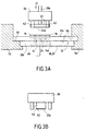
- the tool 22 referenced 22a can be consisting of a semi-cylindrical surface, the length of which is preferably at least equal to that of the electronic module and whose radius of curvature is about a millimeter.
- the test tool 22b shown in FIG. 3b, consists of a cylinder 50 with a diameter preferably equal to about 4 mm and the active end face of which is covered by a layer of silicone or similar material 52 thick about 0.8 mm.
- the bearing surface of the tool 22b is of the order of the surface of the coating drop covering the semiconductor wafer included in the electronic module.
- the silicone layer allows advantageously to absorb the contact of the test tool with the module electronic.
- These two tools 22a and 22b are used on the two main faces 12a and 12b of a card.
- FIG. 3a the mechanical part of the test device.
- Exhibit 54 presents a groove 56 for engaging an edge of the card body 12, while the part 52 has a shoulder 58 on which the other edge of the card rests.
- a stop not shown, ensures the longitudinal positioning of the card.
- Connection pads electric 60 are provided between the longitudinal elements 18 and 20 to ensure the electrical connection between the circuits of the card and circuits 34 of the machine test when the upper face 12a rests on the longitudinal elements of support, that is to say when testing the card by applying the force F on the second side of the card.
- test apparatus described according to the invention allows also to test a card without necessarily going as far as a break. That allows to test cards that work functionally but one of which constituent elements is broken. We deform the card by applying a light constraint without going as far as a rupture. If the card still works, this means say it is not broken. Otherwise, it is broken and rejected.
Landscapes
- Physics & Mathematics (AREA)
- General Physics & Mathematics (AREA)
- Credit Cards Or The Like (AREA)
- Tests Of Electronic Circuits (AREA)
- Techniques For Improving Reliability Of Storages (AREA)
- Testing Or Measuring Of Semiconductors Or The Like (AREA)
- Electrochromic Elements, Electrophoresis, Or Variable Reflection Or Absorption Elements (AREA)
- Electrically Operated Instructional Devices (AREA)
Abstract
Description
- des moyens de supportage et de positionnement de la carte comprenant deux éléments longitudinaux de supportage d'une face de la carte disposés de telle manière que ledit module électronique soit placé entre lesdits éléments longitudinaux,
- un outil mobile selon une direction orthogonale au plan du corps de carte pour appliquer au droit dudit module électronique une force d'intensité croissante,
- des moyens de contrôle pour appliquer audit module électronique des , signaux électriques de commande et pour recevoir les signaux délivrés par ledit module en réponse auxdits signaux de commande,
- des moyens de test pour comparer les signaux reçus à des signaux de référence de fonctionnement correct des circuits intégrés du module électronique, et pour enregistrer au moins l'intensité de la force appliquée par l'outil lorsque les signaux reçus deviennent différents des signaux de référence.
- on soumet la carte à une contrainte en flexion et en compression en positionnant la carte sur des moyens de supportage et de positionnement comprenant deux éléments longitudinaux de supportage d'une face de la carte disposés de telle manière que ledit module électronique soit placé entre lesdits éléments longitudinaux, et en appliquant, au moyen d'un outil mobile selon une direction orthogonale au plan du corps de carte au droit dudit module électronique, une force d'intensité croissante,
- grâce à des moyens de contrôle, on applique audit module électronique des signaux électriques de commande et on reçoit les signaux délivrés par ledit module en réponse auxdits signaux de commande,
- on compare les signaux reçus à des signaux de référence de fonctionnement correct des circuits intégrés du module électronique, et on enregistre au moins l'intensité de la force appliquée par l'outil lorsque les signaux reçus deviennent différents des signaux de référence.
- la figure 1 est une vue de dessus simplifiée montrant une carte placée dans l'appareil de test ;
- la figure 2 est une vue simplifiée de l'ensemble de l'appareil de test ;
- la figure 3a est une vue plus détaillée de l'appareil de test utilisant un premier outil de test ; et
- la figure 3b est une vue partielle montrant un deuxième outil de test utilisable dans l'appareil.
Claims (20)
- Appareil de test pour cartes à mémoire électronique comprenant un corps de carte présentant une première et une deuxième face et un module électronique comportant une pastille semi-conductrice dans laquelle sont réalisés des circuits intégrés, et une pluralité de plages externes de contact électrique raccordées à ladite pastille et disposées dans ladite première face, ledit appareil se caractérisant en ce qu'il comprend :des moyens de supportage et de positionnement de la carte comprenant deux éléments longitudinaux de supportage d'une face de la carte disposés de telle manière que ledit module électronique soit placé entre lesdits éléments longitudinaux,un outil mobile selon une direction orthogonale au plan du corps de carte pour appliquer au droit dudit module électronique une force d'intensité croissante,des moyens de contrôle pour appliquer audit module électronique des signaux électriques de commande et pour recevoir les signaux délivrés par ledit module en réponse auxdits signaux de commande,des moyens de test pour comparer les signaux reçus à des signaux de référence de fonctionnement correct des circuits intégrés du module électronique, et pour enregistrer au moins l'intensité de la force appliquée par l'outil lorsque les signaux reçus deviennent différents des signaux de référence.
- Appareil de test selon la revendication 1, caractérisé en ce qu'il comporte en outre :des moyens pour alimenter ledit module électronique.
- Appareil de test selon la revendication 2, caractérisé en ce qu'il comporte en outre :des moyens de connexion pour relier en permanence les plages externes de la carte aux moyens d'alimentation et de contrôle.
- Appareil de test selon l'une quelconque des revendications 1 à 3, caractérisé en ce qu'il comporte en outre :des moyens pour appliquer audit outil ladite force.
- Appareil de test selon l'une quelconque des revendications 1 à 4, caractérisé en ce que les moyens de test comprennent en outre des moyens pour enregistrer la valeur de la course de l'outil lorsque lesdits signaux reçus sont différents des signaux de référence.
- Appareil de test selon l'une quelconque des revendications 1 à 5, caractérisé en ce que la partie de l'outil destinée à être appliquée sur la carte au droit du module électronique a la forme d'une surface hémicylindrique de faible rayon.
- Appareil de test selon l'une quelconque des revendications 1 à 5, caractérisé en ce que la partie de l'outil destinée à être appliquée sur la carte au droit d'un module électronique est une surface plane circulaire recouverte par une couche d'un matériau légèrement déformable.
- Appareil de test selon l'une quelconque des revendications 3 à 7, caractérisé en ce que lesdits moyens de connexion comprennent des contacts électriques solidaires des moyens pour appliquer la force afin d'établir la connexion électrique avec les plages externes de la carte lorsque celle-ci repose sur les éléments longitudinaux de supportage par sa deuxième face.
- Appareil de test selon l'une quelconque des revendications 3 à 8, caractérisé en ce que lesdits moyens de connexion comprennent des contacts électriques fixes disposés entre les deux éléments longitudinaux de supportage pour établir une connexion électrique avec les plages externes de la carte lorsque ladite carte repose sur les éléments longitudinaux de supportage par sa première face.
- Appareil de test selon l'une quelconque des revendications 1 à 9, caractérisé en ce que lesdits éléments de supportage longitudinaux ont une forme cylindrique.
- Procédé de test pour cartes à mémoire électronique comprenant un corps de carte présentant une première et une deuxième face et un module électronique comportant une pastille semi-conductrice dans laquelle sont réalisés des circuits intégrés, et une pluralité de plages externes de contact électrique raccordées à ladite pastille et disposées dans ladite première face, caractérisé en ce qu'il comporte les étapes selon lesquelles :on soumet la carte à une contrainte en flexion et en compression en positionnant la carte sur des moyens de supportage et de positionnement comprenant deux éléments longitudinaux de supportage d'une face de la carte disposés de telle manière que ledit module électronique soit placé entre lesdits éléments longitudinaux, et en appliquant, au moyen d'un outil mobile selon une direction orthogonale au plan du corps de carte au droit dudit module électronique, une force d'intensité croissante,grâce à des moyens de contrôle, on applique audit module électronique des signaux électriques de commande et on reçoit les signaux délivrés par ledit module en réponse auxdits signaux de commande,on compare les signaux reçus à des signaux de référence de fonctionnement correct des circuits intégrés du module électronique, et on enregistre au moins l'intensité de la force appliquée par l'outil lorsque les signaux reçus deviennent différents des signaux de référence.
- Procédé de test selon la revendication 11, caractérisé en ce qu'il comporte une étape supplémentaire selon laquelle on alimente ledit module électronique grâce à des moyens d'alimentation.
- Procédé de test selon la revendication 12, caractérisé en ce qu'il comporte une étape supplémentaire selon laquelle on connecte en permanence les plages externes de la carte aux moyens d'alimentation et de contrôle, grâce à des moyens de connexion.
- Procédé de test selon l'une quelconque des revendications 11 à 13, caractérisé en ce qu'on utilise des moyens pour appliquer audit outil ladite force.
- Procédé de test selon l'une quelconque des revendications 11 à 14, caractérisé en ce qu'il comporte une étape supplémentaire selon laquelle on enregistre la valeur de la course de l'outil lorsque lesdits signaux reçus sont différents des signaux de référence.
- Procédé de test selon l'une quelconque des revendications 11 à 15, caractérisé en ce que la partie de l'outil destinée à être appliquée sur la carte au droit du module électronique a la forme d'une surface hémicylindrique de faible rayon.
- Procédé de test selon l'une quelconque des revendications 11 et 15, caractérisé en ce que la partie de l'outil destinée à être appliquée sur la carte au droit d'un module électronique est une surface plane circulaire recouverte par une couche d'un matériau légèrement déformable.
- Procédé de test selon l'une quelconque des revendications 13 à 17, caractérisé en ce que lesdits moyens de connexion comprennent des contacts électriques solidaires des moyens pour appliquer la force afin d'établir la connexion électrique avec les plages externes de la carte lorsque celle-ci repose sur les éléments longitudinaux de supportage par sa deuxième face.
- Procédé de test selon l'une quelconque des revendications 13 à 18, caractérisé en ce que lesdits moyens de connexion comprennent des contacts électriques fixes disposés entre les deux éléments longitudinaux de supportage pour établir une connexion électrique avec les plages externes de la carte lorsque ladite carte repose sur les éléments longitudinaux de supportage par sa première face.
- Procédé de test selon l'une quelconque des revendications 11 à 19, caractérisé en ce que lesdits éléments de supportage longitudinaux ont une forme cylindrique.
Applications Claiming Priority (2)
| Application Number | Priority Date | Filing Date | Title |
|---|---|---|---|
| FR9813501A FR2785393B1 (fr) | 1998-10-28 | 1998-10-28 | Appareil de test pour cartes a memoire electronique |
| FR9813501 | 1998-10-28 |
Publications (2)
| Publication Number | Publication Date |
|---|---|
| EP0997740A1 true EP0997740A1 (fr) | 2000-05-03 |
| EP0997740B1 EP0997740B1 (fr) | 2006-05-31 |
Family
ID=9532079
Family Applications (1)
| Application Number | Title | Priority Date | Filing Date |
|---|---|---|---|
| EP99402687A Expired - Lifetime EP0997740B1 (fr) | 1998-10-28 | 1999-10-28 | Appareil de test pour cartes à mémoire électronique |
Country Status (5)
| Country | Link |
|---|---|
| EP (1) | EP0997740B1 (fr) |
| CN (1) | CN1144150C (fr) |
| AT (1) | ATE328287T1 (fr) |
| DE (1) | DE69931575T2 (fr) |
| FR (1) | FR2785393B1 (fr) |
Cited By (2)
| Publication number | Priority date | Publication date | Assignee | Title |
|---|---|---|---|---|
| WO2015019019A1 (fr) * | 2013-08-07 | 2015-02-12 | Oberthur Technologies | Procede de test de resistance d'une carte a puce et dispositif pour la realisation d'un tel test |
| WO2019246075A1 (fr) * | 2018-06-20 | 2019-12-26 | Dish Network L.L.C. | Procédé et appareil de essai de flexion de composants électroniques |
Families Citing this family (2)
| Publication number | Priority date | Publication date | Assignee | Title |
|---|---|---|---|---|
| CN1300833C (zh) * | 2004-09-10 | 2007-02-14 | 华中科技大学 | 集成电路芯片视觉对准方法 |
| CN1912571B (zh) * | 2005-08-12 | 2010-05-26 | 大唐微电子技术有限公司 | 一种测量ic卡模块抗压强度的方法及测量仪 |
Citations (3)
| Publication number | Priority date | Publication date | Assignee | Title |
|---|---|---|---|---|
| WO1979000543A1 (fr) * | 1978-01-24 | 1979-08-09 | R Moreno | Procede et dispositif pour connecter electriquement un objet amovible notamment une carte electronique portative |
| JPS58127176A (ja) * | 1982-01-26 | 1983-07-28 | Nec Corp | 電気的接続試験方式 |
| JPS58166272A (ja) * | 1982-03-27 | 1983-10-01 | Hitachi Ltd | コネクタ接触子の接触信頼度評価装置 |
Family Cites Families (2)
| Publication number | Priority date | Publication date | Assignee | Title |
|---|---|---|---|---|
| FR2725290B1 (fr) * | 1994-09-30 | 1996-12-20 | Trt Telecom Radio Electr | Dispositif et procede de test mecanique de cartes a circuit(s) integre(s) |
| DE19620550C1 (de) * | 1996-05-22 | 1997-10-16 | Orga Kartensysteme Gmbh | Verfahren zum Testen der elektrischen Funktionstüchtigkeit einer kontaktbehafteten Chipkarte und Vorrichtung zum Durchführen des Verfahrens |
-
1998
- 1998-10-28 FR FR9813501A patent/FR2785393B1/fr not_active Expired - Fee Related
-
1999
- 1999-10-27 CN CNB991233840A patent/CN1144150C/zh not_active Expired - Fee Related
- 1999-10-28 AT AT99402687T patent/ATE328287T1/de not_active IP Right Cessation
- 1999-10-28 EP EP99402687A patent/EP0997740B1/fr not_active Expired - Lifetime
- 1999-10-28 DE DE69931575T patent/DE69931575T2/de not_active Expired - Fee Related
Patent Citations (3)
| Publication number | Priority date | Publication date | Assignee | Title |
|---|---|---|---|---|
| WO1979000543A1 (fr) * | 1978-01-24 | 1979-08-09 | R Moreno | Procede et dispositif pour connecter electriquement un objet amovible notamment une carte electronique portative |
| JPS58127176A (ja) * | 1982-01-26 | 1983-07-28 | Nec Corp | 電気的接続試験方式 |
| JPS58166272A (ja) * | 1982-03-27 | 1983-10-01 | Hitachi Ltd | コネクタ接触子の接触信頼度評価装置 |
Non-Patent Citations (2)
| Title |
|---|
| PATENT ABSTRACTS OF JAPAN vol. 7, no. 241 (P - 232)<1386> 26 October 1983 (1983-10-26) * |
| PATENT ABSTRACTS OF JAPAN vol. 8, no. 1 (P - 246)<1438> 6 January 1984 (1984-01-06) * |
Cited By (4)
| Publication number | Priority date | Publication date | Assignee | Title |
|---|---|---|---|---|
| WO2015019019A1 (fr) * | 2013-08-07 | 2015-02-12 | Oberthur Technologies | Procede de test de resistance d'une carte a puce et dispositif pour la realisation d'un tel test |
| FR3009617A1 (fr) * | 2013-08-07 | 2015-02-13 | Oberthur Technologies | Procede de test de resistance d'une carte a puce et dispositif pour la realisation d'un tel test |
| WO2019246075A1 (fr) * | 2018-06-20 | 2019-12-26 | Dish Network L.L.C. | Procédé et appareil de essai de flexion de composants électroniques |
| US10768219B2 (en) | 2018-06-20 | 2020-09-08 | Dish Network L.L.C. | Method and apparatus for flexure testing of electronic components |
Also Published As
| Publication number | Publication date |
|---|---|
| DE69931575T2 (de) | 2007-05-10 |
| CN1144150C (zh) | 2004-03-31 |
| CN1252583A (zh) | 2000-05-10 |
| EP0997740B1 (fr) | 2006-05-31 |
| FR2785393B1 (fr) | 2001-01-19 |
| DE69931575D1 (de) | 2006-07-06 |
| FR2785393A1 (fr) | 2000-05-05 |
| ATE328287T1 (de) | 2006-06-15 |
Similar Documents
| Publication | Publication Date | Title |
|---|---|---|
| EP0645626B1 (fr) | Dispositif de mesure pour capteurs amovibles | |
| FR2914422A1 (fr) | Procede de detection de defauts de surface d'un substrat et dispositif mettant en oeuvre ledit procede. | |
| EP1177766B1 (fr) | Procédé d'acquisition d'une image d'une zone non dermatoglyphique de la peau au moyen d'un dispositif d'acquisition comprenant un capteur non optique. | |
| WO2010029179A1 (fr) | Dispositif d'indentation continue ou instrumentee a surface de support convexe et son utilisation, notamment pour l'indentation de toles | |
| EP0997740B1 (fr) | Appareil de test pour cartes à mémoire électronique | |
| EP1157261B1 (fr) | Procede et dispositif d'analyse d'un front d'onde a grande dynamique | |
| FR2477324A1 (fr) | Dispositif de contact electrique pour appareil de traitement de cartes electroniques | |
| EP0704819B1 (fr) | Dispositif et procédé de test mécanique de cartes de circuit(s) intégré(s) | |
| EP2960657A1 (fr) | Procede de caracterisation d'un dispositif de connexion electrique destine a etre contacte a un dispositif electronique | |
| FR2617977A1 (fr) | Appareil de test de circuit imprime | |
| EP0147245A2 (fr) | Dispositif et procédé de contrôle de continuité des circuits imprimés | |
| EP0354080A1 (fr) | Adaptateur de brochage pour le test de circuits imprimés de haute densité | |
| FR3089070A1 (fr) | Dispositif de contrôle du verrouillage d’un conducteur à un connecteur, système d’aide au contrôle du verrouillage d’un conducteur à un connecteur et procédé d’utilisation d’un tel système | |
| WO2014195429A1 (fr) | Dispositif de capture d'une image représentative d'une empreinte d'une partie du corps d'une personne | |
| WO2000066996A1 (fr) | Procede et dispositif de vieillissement accelere de cartes en matiere plastique du type des cartes a puce | |
| FR2619927A1 (fr) | Procede de verification des trous metallises d'une carte de circuit imprime multicouche et dispositif de mise en oeuvre | |
| FR2718522A1 (fr) | Dispositif pour effectuer la mesure d'un profil sur une surface plane. | |
| EP0483008B1 (fr) | Dispositif de glantage à platine pivotante | |
| FR3009617B1 (fr) | Procede de test de resistance d'une carte a puce et dispositif pour la realisation d'un tel test | |
| WO2002084313A1 (fr) | Sonde et dispositif de mesure | |
| FR3037651A1 (fr) | Capteur et systeme traceur de temperature en environnement a fortes accelerations | |
| WO2024133832A1 (fr) | Dispositif piézoélectrique | |
| FR2555338A1 (fr) | Appareil destine a identifier et indiquer la reference d'une pile electrique dans une marque donnee de piles | |
| FR3143862A1 (fr) | Dispositif et procédé de détection d’une déformation d’un emballage d’une cellule de batterie | |
| FR3150070A1 (fr) | carte électronique pour ensemble modulaire électrique |
Legal Events
| Date | Code | Title | Description |
|---|---|---|---|
| PUAI | Public reference made under article 153(3) epc to a published international application that has entered the european phase |
Free format text: ORIGINAL CODE: 0009012 |
|
| AK | Designated contracting states |
Kind code of ref document: A1 Designated state(s): AT BE CH CY DE DK ES FI FR GB GR IE IT LI LU MC NL PT SE |
|
| AX | Request for extension of the european patent |
Free format text: AL;LT;LV;MK;RO;SI |
|
| 17P | Request for examination filed |
Effective date: 20000918 |
|
| AKX | Designation fees paid |
Free format text: AT BE CH CY DE DK ES FI FR GB GR IE IT LI LU MC NL PT SE |
|
| RAP1 | Party data changed (applicant data changed or rights of an application transferred) |
Owner name: AXALTO S.A. |
|
| GRAP | Despatch of communication of intention to grant a patent |
Free format text: ORIGINAL CODE: EPIDOSNIGR1 |
|
| RIC1 | Information provided on ipc code assigned before grant |
Ipc: 7G 01N 3/20 B Ipc: 7G 06K 19/077 B Ipc: 7G 01R 31/04 A |
|
| GRAS | Grant fee paid |
Free format text: ORIGINAL CODE: EPIDOSNIGR3 |
|
| GRAA | (expected) grant |
Free format text: ORIGINAL CODE: 0009210 |
|
| RIN1 | Information on inventor provided before grant (corrected) |
Inventor name: LIMELETTE, YANN Inventor name: REIGNOUX, YVES |
|
| AK | Designated contracting states |
Kind code of ref document: B1 Designated state(s): AT BE CH CY DE DK ES FI FR GB GR IE IT LI LU MC NL PT SE |
|
| PG25 | Lapsed in a contracting state [announced via postgrant information from national office to epo] |
Ref country code: NL Free format text: LAPSE BECAUSE OF FAILURE TO SUBMIT A TRANSLATION OF THE DESCRIPTION OR TO PAY THE FEE WITHIN THE PRESCRIBED TIME-LIMIT Effective date: 20060531 Ref country code: IT Free format text: LAPSE BECAUSE OF FAILURE TO SUBMIT A TRANSLATION OF THE DESCRIPTION OR TO PAY THE FEE WITHIN THE PRESCRIBED TIME-LIMIT;WARNING: LAPSES OF ITALIAN PATENTS WITH EFFECTIVE DATE BEFORE 2007 MAY HAVE OCCURRED AT ANY TIME BEFORE 2007. THE CORRECT EFFECTIVE DATE MAY BE DIFFERENT FROM THE ONE RECORDED. Effective date: 20060531 Ref country code: IE Free format text: LAPSE BECAUSE OF FAILURE TO SUBMIT A TRANSLATION OF THE DESCRIPTION OR TO PAY THE FEE WITHIN THE PRESCRIBED TIME-LIMIT Effective date: 20060531 Ref country code: GB Free format text: LAPSE BECAUSE OF FAILURE TO SUBMIT A TRANSLATION OF THE DESCRIPTION OR TO PAY THE FEE WITHIN THE PRESCRIBED TIME-LIMIT Effective date: 20060531 Ref country code: FI Free format text: LAPSE BECAUSE OF FAILURE TO SUBMIT A TRANSLATION OF THE DESCRIPTION OR TO PAY THE FEE WITHIN THE PRESCRIBED TIME-LIMIT Effective date: 20060531 Ref country code: AT Free format text: LAPSE BECAUSE OF FAILURE TO SUBMIT A TRANSLATION OF THE DESCRIPTION OR TO PAY THE FEE WITHIN THE PRESCRIBED TIME-LIMIT Effective date: 20060531 |
|
| REG | Reference to a national code |
Ref country code: GB Ref legal event code: FG4D Free format text: NOT ENGLISH Ref country code: CH Ref legal event code: EP |
|
| REG | Reference to a national code |
Ref country code: IE Ref legal event code: FG4D Free format text: LANGUAGE OF EP DOCUMENT: FRENCH |
|
| REF | Corresponds to: |
Ref document number: 69931575 Country of ref document: DE Date of ref document: 20060706 Kind code of ref document: P |
|
| PG25 | Lapsed in a contracting state [announced via postgrant information from national office to epo] |
Ref country code: SE Free format text: LAPSE BECAUSE OF FAILURE TO SUBMIT A TRANSLATION OF THE DESCRIPTION OR TO PAY THE FEE WITHIN THE PRESCRIBED TIME-LIMIT Effective date: 20060831 Ref country code: DK Free format text: LAPSE BECAUSE OF FAILURE TO SUBMIT A TRANSLATION OF THE DESCRIPTION OR TO PAY THE FEE WITHIN THE PRESCRIBED TIME-LIMIT Effective date: 20060831 |
|
| PG25 | Lapsed in a contracting state [announced via postgrant information from national office to epo] |
Ref country code: ES Free format text: LAPSE BECAUSE OF FAILURE TO SUBMIT A TRANSLATION OF THE DESCRIPTION OR TO PAY THE FEE WITHIN THE PRESCRIBED TIME-LIMIT Effective date: 20060911 |
|
| PG25 | Lapsed in a contracting state [announced via postgrant information from national office to epo] |
Ref country code: PT Free format text: LAPSE BECAUSE OF FAILURE TO SUBMIT A TRANSLATION OF THE DESCRIPTION OR TO PAY THE FEE WITHIN THE PRESCRIBED TIME-LIMIT Effective date: 20061031 Ref country code: MC Free format text: LAPSE BECAUSE OF NON-PAYMENT OF DUE FEES Effective date: 20061031 Ref country code: LI Free format text: LAPSE BECAUSE OF NON-PAYMENT OF DUE FEES Effective date: 20061031 Ref country code: CH Free format text: LAPSE BECAUSE OF NON-PAYMENT OF DUE FEES Effective date: 20061031 |
|
| NLV1 | Nl: lapsed or annulled due to failure to fulfill the requirements of art. 29p and 29m of the patents act | ||
| GBV | Gb: ep patent (uk) treated as always having been void in accordance with gb section 77(7)/1977 [no translation filed] |
Effective date: 20060531 |
|
| PLBE | No opposition filed within time limit |
Free format text: ORIGINAL CODE: 0009261 |
|
| STAA | Information on the status of an ep patent application or granted ep patent |
Free format text: STATUS: NO OPPOSITION FILED WITHIN TIME LIMIT |
|
| 26N | No opposition filed |
Effective date: 20070301 |
|
| REG | Reference to a national code |
Ref country code: CH Ref legal event code: PL |
|
| BERE | Be: lapsed |
Owner name: AXALTO S.A. Effective date: 20061031 |
|
| PG25 | Lapsed in a contracting state [announced via postgrant information from national office to epo] |
Ref country code: GR Free format text: LAPSE BECAUSE OF FAILURE TO SUBMIT A TRANSLATION OF THE DESCRIPTION OR TO PAY THE FEE WITHIN THE PRESCRIBED TIME-LIMIT Effective date: 20060901 |
|
| PG25 | Lapsed in a contracting state [announced via postgrant information from national office to epo] |
Ref country code: LU Free format text: LAPSE BECAUSE OF NON-PAYMENT OF DUE FEES Effective date: 20061028 |
|
| PG25 | Lapsed in a contracting state [announced via postgrant information from national office to epo] |
Ref country code: CY Free format text: LAPSE BECAUSE OF FAILURE TO SUBMIT A TRANSLATION OF THE DESCRIPTION OR TO PAY THE FEE WITHIN THE PRESCRIBED TIME-LIMIT Effective date: 20060531 |
|
| PGFP | Annual fee paid to national office [announced via postgrant information from national office to epo] |
Ref country code: DE Payment date: 20081030 Year of fee payment: 10 |
|
| PGFP | Annual fee paid to national office [announced via postgrant information from national office to epo] |
Ref country code: FR Payment date: 20081028 Year of fee payment: 10 |
|
| PG25 | Lapsed in a contracting state [announced via postgrant information from national office to epo] |
Ref country code: BE Free format text: LAPSE BECAUSE OF FAILURE TO SUBMIT A TRANSLATION OF THE DESCRIPTION OR TO PAY THE FEE WITHIN THE PRESCRIBED TIME-LIMIT Effective date: 20061031 |
|
| REG | Reference to a national code |
Ref country code: FR Ref legal event code: ST Effective date: 20100630 |
|
| PG25 | Lapsed in a contracting state [announced via postgrant information from national office to epo] |
Ref country code: FR Free format text: LAPSE BECAUSE OF NON-PAYMENT OF DUE FEES Effective date: 20091102 Ref country code: DE Free format text: LAPSE BECAUSE OF NON-PAYMENT OF DUE FEES Effective date: 20100501 |