EP0997964A2 - Dielektrisches Filter, dielektrischer Duplexer und Kommunikationsgerät - Google Patents
Dielektrisches Filter, dielektrischer Duplexer und Kommunikationsgerät Download PDFInfo
- Publication number
- EP0997964A2 EP0997964A2 EP99121259A EP99121259A EP0997964A2 EP 0997964 A2 EP0997964 A2 EP 0997964A2 EP 99121259 A EP99121259 A EP 99121259A EP 99121259 A EP99121259 A EP 99121259A EP 0997964 A2 EP0997964 A2 EP 0997964A2
- Authority
- EP
- European Patent Office
- Prior art keywords
- face
- holes
- external coupling
- faces
- external
- Prior art date
- Legal status (The legal status is an assumption and is not a legal conclusion. Google has not performed a legal analysis and makes no representation as to the accuracy of the status listed.)
- Granted
Links
Images



Classifications
-
- H—ELECTRICITY
- H01—ELECTRIC ELEMENTS
- H01P—WAVEGUIDES; RESONATORS, LINES, OR OTHER DEVICES OF THE WAVEGUIDE TYPE
- H01P7/00—Resonators of the waveguide type
- H01P7/10—Dielectric resonators
-
- H—ELECTRICITY
- H01—ELECTRIC ELEMENTS
- H01P—WAVEGUIDES; RESONATORS, LINES, OR OTHER DEVICES OF THE WAVEGUIDE TYPE
- H01P1/00—Auxiliary devices
- H01P1/20—Frequency-selective devices, e.g. filters
- H01P1/213—Frequency-selective devices, e.g. filters combining or separating two or more different frequencies
- H01P1/2136—Frequency-selective devices, e.g. filters combining or separating two or more different frequencies using comb or interdigital filters; using cascaded coaxial cavities
-
- H—ELECTRICITY
- H01—ELECTRIC ELEMENTS
- H01P—WAVEGUIDES; RESONATORS, LINES, OR OTHER DEVICES OF THE WAVEGUIDE TYPE
- H01P1/00—Auxiliary devices
- H01P1/20—Frequency-selective devices, e.g. filters
- H01P1/201—Filters for transverse electromagnetic waves
- H01P1/205—Comb or interdigital filters; Cascaded coaxial cavities
-
- H—ELECTRICITY
- H01—ELECTRIC ELEMENTS
- H01P—WAVEGUIDES; RESONATORS, LINES, OR OTHER DEVICES OF THE WAVEGUIDE TYPE
- H01P1/00—Auxiliary devices
- H01P1/20—Frequency-selective devices, e.g. filters
- H01P1/201—Filters for transverse electromagnetic waves
- H01P1/205—Comb or interdigital filters; Cascaded coaxial cavities
- H01P1/2056—Comb filters or interdigital filters with metallised resonator holes in a dielectric block
-
- H—ELECTRICITY
- H01—ELECTRIC ELEMENTS
- H01P—WAVEGUIDES; RESONATORS, LINES, OR OTHER DEVICES OF THE WAVEGUIDE TYPE
- H01P1/00—Auxiliary devices
- H01P1/20—Frequency-selective devices, e.g. filters
- H01P1/213—Frequency-selective devices, e.g. filters combining or separating two or more different frequencies
Definitions
- the present invention relates to a dielectric filter, used for instance in a microwave band, a dielectric duplexer, and a communication apparatus using these.
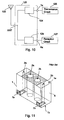
- Fig. 11 shows a structure of this type of conventional dielectric filter.
- shaded portions represent portions where the bare outside of the dielectric block (nonconductive portions) can be seen.
- This dielectric filter comprises resonator holes 2a and 2b, and external coupling holes 3a and 3b, provided from a first end face 1a of a dielectric block 1 passing to a second end face 1b opposite thereto, inner conductors being provided on the inner faces of these holes, and an external conductor 6 being provided on the outer face of the dielectric block 1.
- Unformed portions of the external conductor 6 are provided at the opening regions of the resonator holes 2a and 2b in the first end face 1a, and the inner conductors of the resonator holes 2a and 2b are isolated from the external conductor 6 by the first end face 1a, but lead to the external conductor 6 on the second end face 1b.
- the external conductor 6 is provided at the opening regions of the external coupling holes 3a and 3b in the first end face 1a, and the inner conductors in the external coupling holes 3a and 3b lead to the external conductor 6 at the first end face 1a.
- input/output electrodes 7a and 7b are isolated from the external conductor 6, and are provided across the second end face 1b and one side face, leading to the inner conductors of the external coupling holes 3a and 3b.
- the inner conductors of the resonator holes 2a and 2b are combline-coupled, the inner conductors of the external coupling holes 3a and 3b are interdigitally coupled to their respective adjacent resonator holes 2a and 2b, and this electromagnetic field coupling achieves an external coupling.
- This dielectric filter is manufactured by using nonelectrolytic plating to provide an electrode material on all the outer faces of the dielectric block, comprising resonator holes and external coupling holes, and in all the inner faces of the holes; thereafter, the external conductor at the opening region of the resonator holes on the first side face, and the external conductor around the input/output electrode are removed. This removal of the resonator holes opening region of the first side face is performed by removing the external conductors using sandpaper or the like.
- the open face of one resonator hole of adjacent resonator holes is provided at a first end face
- the open face of the other resonator hole is provided at a second end face
- the adjacent resonator holes are interdigitally coupled, external conductor formed regions and unformed regions are needed on both end faces.
- the external conductors may be formed on the end faces by a screen printing method, but in this case, the number of manufacturing processes such as conductor paste printing, conductor heating, and the like, is increased, and furthermore, there is a problem that positional deviation, wrinkling of the conductor paste, and the like, will adversely affect the positional precision of the external conductors.
- preferred embodiments of the present invention provide a dielectric filter, a dielectric duplexer, and a communication apparatus using these, wherein open faces of resonator holes can be formed by a simple operation and with high dimensional precision, and which are consequently inexpensive and have superior characteristics.
- One preferred embodiment of the present invention provides a dielectric filter or a dielectric duplexer, comprising: a dielectric block having a first end face and a second end face and side faces extending therebetween; a plurality of resonator holes and at least one external coupling hole respectively passing through both end faces; inner conductors provided on inner faces of the resonator holes and the external coupling holes; an external conductor provided on the outer faces of the dielectric block; concavities provided in formation regions of the external coupling holes on the first and the second end face and in the short-circuiting regions of the resonator holes; and the external conductor being removed except from the portions of the concavities in the first end face and the second end face, thereby forming open faces of the resonator holes on the first end face and the second end face.
- the concavities are provided in the formation regions of the external coupling holes on the first end face, and the external conductor is removed except from the portions of the concavities in the first end face, thereby forming open faces of the resonator holes on the first end face.
- the dielectric filter and the dielectric duplexer comprise external coupling adjustment holes, passing through the concavities in the external coupling holes formation region on the first end face and the second end face, and inner conductors are provided on the inner faces thereof.
- the opening portions of the external coupling holes in the concavities, and the opening faces of the external coupling adjustment holes may be provided at different positions along the axial directions of the holes.
- the size of the external coupling can be adjusted by changing the shape of the diameter and the arrangement position of the external coupling holes and the external coupling adjustment holes.
- the external coupling adjustment holes have a function of cutting off couplings between adjacent resonator holes on either side thereof.
- by changing the shape and depth of the concavities, and changing the length (axial length) of the external coupling holes and the external coupling adjustment holes it is possible to increase the freedom with which the size of the external coupling can be adjusted and set.
- an even greater external coupling can be obtained by connecting input/output electrodes to the inner conductors in the external coupling holes on the second end face, the input/output electrodes being isolated from the external conductor, and interdigitally coupling the inner conductors in the external coupling holes to the inner conductors in adjacent resonator holes. Furthermore, if the input/output electrodes are provided crossing to a side face, the side face on which the input/output electrodes are provided can be a surface mount face.
- external coupling means comprising external coupling holes is applied to at least one input/output portion of multiple input and output portions, and the external coupling of the other input/output portions is achieved by the capacitance coupling of the input/output electrodes to the external coupling holes.
- the input/output electrodes may be connected to the inner conductors in the external coupling holes on the first end face, and isolated from the external conductor, and the inner conductors of the external coupling holes and the inner conductors in the resonator holes adjacent thereto can be combline coupled.
- the inner conductors of the external coupling holes can be isolated from the external conductor on one end face, without providing input/output electrodes, and metallic input/output terminals which connect to the inner conductors of the external coupling holes can then be inserted.
- a communication apparatus comprises the dielectric filter and the dielectric duplexer having the features described above, and therefore, it is inexpensive and has superior characteristics.
- Fig. 1 is a perspective view of a dielectric filter according to a first embodiment.
- Fig. 2 is a perspective view of a manufacturing process of the dielectric filter according to the first embodiment, showing a state when conductors are provided to all faces of a dielectric block.
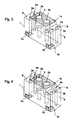
- Fig. 3 is a perspective view of a dielectric filter according to a second embodiment.
- Fig. 4 is a perspective view of a dielectric filter according to a third embodiment.
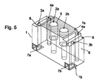
- Fig. 5 is a perspective view of a dielectric filter according to a fourth embodiment.
- Fig. 6 is a perspective view of a dielectric duplexer according to a fifth embodiment.
- Fig. 7 is a perspective view of a dielectric duplexer according to a sixth embodiment.
- Fig. 8 is a perspective view of a dielectric filter according to a seventh embodiment.
- Fig. 9 is a perspective view of a dielectric duplexer according to an eighth embodiment.
- Fig. 10 is a block diagram of a communication apparatus according to a ninth embodiment.
- Fig. 11 is a perspective view of a prior art dielectric filter.
- Fig. 1 is a perspective view of a dielectric filter, and shows open faces of resonator holes at the top, and a mount face to a circuit substrate at the front.
- the dielectric filter of the present embodiment comprises holes and electrodes of predetermined shapes provided on a substantially rectangular dielectric block 1, comprising a dielectric ceramic.
- Resonator holes 2a and 2b, and external coupling holes 3a and 3b are provided passing through from a first end face 1a of the dielectric block 1 to a second end face 1b opposite thereto, so that their axes are parallel to each other, and concavities 8 are provided at the formation regions of the external coupling holes 3a and 3b on the first end face 1a.
- the concavities 8 are positioned on both sides of the first end face 1a, and are formed by notching rectangular shapes in the three side faces.
- the diameters of the resonator holes 2a and 2b are large one the first end face 1a side, and small on the second end face 1b, forming step holes.
- the diameters of the external coupling holes 3a and 3b are the same along their entire lengths, forming straight holes.
- Inner conductors 5 are provided in the holes 2a, 2b, 3a, and 3b.
- An external conductor 6 is provided substantially over the entire outer faces of the dielectric block, with the exception of the open faces of the resonator holes 2a and 2b on the first end face 1a, and input/output electrodes 7a and 7b are provided at the openings of the external coupling holes 3a and 3b on the second end face 1b, and are isolated from the external conductor 6.
- the input/output electrodes 7a and 7b are provided across the second end face 1b and the side face, and the side face of this dielectric filter on which the input/output electrodes 7a and 7b are provided is the mount face, which is mounted on a mount substrate.
- the inner conductors 5 of the resonator holes 2a and 2b are isolated from the external conductor 6 on the first end face 1a, and connect to the external conductor 6 on the second end face 1b; the opening faces of the resonator holes 2a and 2b on the first end face 1a being the open faces of the resonator holes 2a and 2b, and the second end face 1b being the short-circuiting face of the resonator holes. That is, on the first end face 1a, the open faces of the resonator holes 2a and 2b are provided at a position projecting out from the other portions.
- the inner conductors 5 of the external coupling holes 3a and 3b are connected to the external conductor 6 on the first end face la (in the concavities 8), and are connected to the input/output electrodes 7a and 7b on the second end face 1b, while being isolated from the external conductor 6. That is, the external coupling holes 3a and 3b are short-circuited on the first end face 1a.
- This dielectric filter comprises two resonators in correspondence with the inner conductors 5 in the resonator holes 2a and 2b, these adjacent resonators being combline coupled, and the inner conductors 5 in the external coupling holes 3a and 3b are interdigitally coupled by an electromagnetic field to the inner conductors 5 of the adjacent resonator holes 2a and 2b, thereby obtaining by this coupling an external coupling.
- electrode material such as Cu and Ag, is provided by nonelectrolytic plating on all surfaces of a dielectric block, and as shown in Fig. 2, inner conductors are provided in the inner faces of the holes 2a, 2b, 3a, and 3b, and an external conductor 6 is provided on all the outer faces, forming the dielectric block 1.
- the first end face 1a is flat-polished by a rotating polisher, sandpaper, or the like, removing the external conductor 6 except from the concavities 8.
- the external conductor 6 around the input/output electrodes 7a and 7b is removed by an ultrasonic processing machine, forming input/output electrodes 7a and 7b which are isolated from the external conductor 6, thereby obtaining the dielectric filter shown in Fig. 1.
- the formation of the concavities 8 may acceptably be performed by cutting after forming and heating the dielectric block.
- the depth of the concavities 8 need only be the depth left by the external conductor 6 when the first end face 1a has been flat-polished; furthermore, the shape of the concavities 8 is not restricted to that shown in the above embodiment. Furthermore, the two concavities 8 do not have to be the same shape.
- the resonator holes are step holes, and the external coupling holes are straight holes, but the resonator holes may be straight holes, and the external coupling holes may be step holes, it being acceptable to mix straight holes and step holes.
- the dielectric filter may acceptably comprise three or more resonators with three or more resonator holes provided in the dielectric block.
- the external coupling holes are provided adjacent to the resonator holes in the input/output stage.
- the concavities 8 are provided at opening regions of the external coupling holes 3a and 3b on the first end face 1a, by the simple operation of polishing the first end face 1a until it is flat, it is possible to leave the external conductor 6 on the concavities 8 forming the openings of the external coupling holes 3a and 3b, while in addition removing the external conductor from all the open faces of the resonator holes 2a and 2b.
- the open faces of the resonator holes 2a and 2b can be provided inexpensively, and in addition, the dimensions of the formation regions and unformed regions of the external conductor 6 (nonconductive portions 6) on the first end face 1a are highly precise, enabling variation in filter characteristics caused by variation in the shape of the external conductor 6 to be greatly reduced.
- the size of the external coupling can also be adjusted and set.
- Fig. 3 shows a constitution of a dielectric filter according to a second embodiment of the present invention.
- the external coupling holes were provided in the concavities of the first side face, but in the present embodiment, in addition to the external coupling holes 3a and 3b, external coupling adjustment holes 4a to 4c are provided passing through the concavities 8 and the second end face 1b, and having inner conductors 5 provided on their inner faces.
- the inner conductors 5 of the external coupling adjustment holes 4a and 4b connect (lead) to the external conductor 6 on both end faces 1a and 1b.
- the rest of the constitution is the same as in the first embodiment, and explanation thereof will be omitted.
- the external coupling adjustment holes 4a and 4b are provided to adjust the external coupling (to weaken the external coupling), and can obtain various external couplings by changing the formation position and shape of the external coupling adjustment holes 4a and 4b.
- the open faces of the resonator holes 2a and 2b can be provided with high precision and simply. Furthermore, the external coupling can be adjusted and set by changing the shape and depth of the concavities 8.
- Fig. 4 shows a constitution of a dielectric filter according to a third embodiment of the present invention.
- the concavities 8 are provided in a step shape, being deep on one side face side and shallow on the other side face side, the external coupling holes 3a and 3b are provided in the deep parts of the concavities, and the external coupling adjustment holes 4a and 4b are provided in the shallow parts. That is, the openings of the external coupling holes 3a and 3b and the external coupling adjustment holes 4a and 4b are provided in different positions in the axial length direction.
- Fig. 5 shows a dielectric filter according to a fourth embodiment of the present invention.
- the concavities 8 are provided in a step shape, being shallow on the resonator holes 2a and 2b side and deep on the side face sides, the external coupling holes 3a and 3b are provided in the deep parts of the concavities, and the external coupling adjustment holes 4a and 4b are provided in the shallow parts.
- This constitution achieves the same effects as the third embodiment.
- Fig. 6 shows a dielectric duplexer (antenna resonator) according to a fifth embodiment of the present invention.
- the dielectric duplexer of the present embodiment comprises a substantially rectangular dielectric block 1, the transmission side comprising a bandpass filter, comprising two-stage resonators in correspondence with the resonator holes 2b and 2c, and a trap resonator in correspondence with the resonator hole 2a, and the reception side comprising a bandpass filter, comprising three-stage resonators in correspondence with the resonator holes 2d to 2f, and a trap resonator in correspondence with the resonator hole 2g.
- the concavities 8 are provided on the first end face 1a of the dielectric block 1 between the resonator holes 2a and 2b, between the resonator holes 2c and 2d, and between the resonator holes 2f and 2g, and external coupling holes 3a, 3b, and 3c, and external coupling adjustment holes 4a, 4b, and 4c, are provided in the regions of the concavities 8.
- the concavities 8 are provided in groove-shapes along opposing side faces.
- Inner conductors 5 are provided on the inner faces of the holes 2a to 2g, 3a, 3b, 3c, 4a, 4b, and 4c.
- An external conductor 6 is provided substantially over all the outer faces of the dielectric block, with the exception of the open faces of the resonator holes 2a to 2g on the first end face 1a.
- the input/output electrodes 7a, 7b, and 7c are provided across the second end face 1b and the side faces, and connect to the inner conductors 5 in the external coupling holes 3a, 3b, and 3c, and are isolated from the external conductor 6.
- the input/output electrode 7a functions as the transmission terminal of a transmission side filter
- the input/output electrode 7c functions as the receive terminal of a transmission side filter
- the input/output electrode 7b functions as an antenna terminal sharing the input and output of the transmission and receive filters.
- the external coupling hole 3a is interdigitally coupled to the adjacent resonator holes 2a and 2b
- the external coupling hole 3b is interdigitally coupled to the adjacent resonator holes 2c and 2d
- the external coupling hole 3c is interdigitally coupled to the adjacent resonator holes 2f and 2g, and these couplings obtain the external coupling.
- the external coupling holes 3a to 3c of the present embodiment also have a function of cutting off couplings between the adjacent resonator holes on either side thereof.
- the concavities 8 are provided in the first end face 1a, enabling the same effects to be achieved as were described in the first and second embodiments.
- Fig. 7 shows a constitution of a dielectric duplexer according to a sixth embodiment of the present invention.
- the dielectric duplexer of the present embodiment comprises a substantially rectangular dielectric block 1, the transmission side comprising a bandpass filter, comprising three-stage resonators in correspondence with the resonator holes 2a, 2b, and 2c, and the reception side comprising a bandpass filter, comprising three-stage resonators in correspondence with the resonator holes 2d to 2f.
- the concavities 8 are provided on the first end face 1a of the dielectric block 1 between the resonator holes 2c and 2d, and an external coupling hole 3b and an external coupling adjustment hole 4b are provided in the regions of the concavities 8.
- Inner conductors 5 are provided on the inner faces of the holes 2a to 2f, 3b, and 4b.
- the external conductor 6 is provided on substantially all faces of the dielectric block 1, excluding the open faces of the holes 2a to 2f on the first end face 1a.
- the input/output electrode 7b which forms the antenna terminal is provided across the second end face 1b and the side face, and the input/output electrode 7a which forms the transmission terminal, and the input/output electrode 7c which forms the receive terminal, are provided near the first end face 1a across to the adjacent side faces.
- the input/output electrodes 7a and 7c are capacitance-coupled to the resonator holes 2a and 2f respectively, these capacitances achieving an external coupling.
- the external coupling hole 3b is interdigitally coupled to the adjacent resonator holes 2c and 2d, and this coupling achieves an external coupling. In this way, external coupling means comprising external coupling holes may be applied to one input/output portion of multiple input and output portions, and in this case, only one concavity needs to be provided in the first end face.
- the concavity is provided in the first end face 1a, enabling the same effects to be achieved as were described in the first and second embodiments.
- the concavities may be provided with a step portion as in the third and fourth embodiments. Furthermore, the external coupling adjustment holes do not necessarily have to be provided.
- the coupling between the external coupling holes and the resonator holes of the input/output stage is an interdigital coupling in order to obtain an even greater external coupling, but it is acceptable to provide the input/output electrodes in the concavities in the first end face and achieve the external coupling by a combline coupling.
- the open faces of the resonator holes were all provided on the first end face, and adjacent resonators were combline coupled, but next, the constitutions of a dielectric filter and a dielectric duplexer in which adjacent resonators are interdigitally coupled will be explained with reference to Fig. 8 and Fig. 9.
- Fig. 8 shows a constitution of a dielectric filter according to a seventh embodiment of the present invention.
- the dielectric filter of the present embodiment comprises concavities 8 provided in the formation regions of the external coupling holes 3a and 3b, and the short-circuiting region of the resonator hole 2b on the first end face 1a, and furthermore, in the formation regions of the external coupling holes 3a and 3b, and the short-circuiting region of the resonator hole 2a on the second end face 1b.
- the opening face of the resonator hole 2a on the first end face 1a, and the opening face of the resonator hole 2b on the second end face 1b, are unformed conductor portions (nonconductive portions), and these faces form the open faces of the resonator holes 2a and 2b. That is, the open face of the resonator hole 2a on the first end face 1a, and the open face of the resonator hole 2b on the second end face 1b, are provided in positions projecting further than other portions.
- the resonator holes 2a and 2b are interdigitally coupled.
- Fig. 9 shows a constitution of a dielectric duplexer according to an eighth embodiment of the present invention.
- the open face of one resonator hole 2e comprising a reception side filter, is provided on the second end face 1b.
- the concavities 8 are provided in portions excluding the formation regions of the external coupling holes 3a to 3c and the external coupling adjustment holes 4a to 4c on the first end face 1a, the short-circuiting region of the resonator hole 2e, and also the open region of the resonator 2e on the second end face 1b.
- the opening faces of the resonator holes 2a to 2d, 2f, and 2g on the first end face 1a, and the opening face of the resonator hole 2e on the second end face 1b, are unformed conductor portions (nonconductive portions), and these faces form the open faces of the resonator holes. That is, the open faces of the resonator holes 2a to 2d, 2f, and 2g on the first end face 1a, and the open face of the resonator hole 2e on the second end face, are provided in positions projecting further than the other portions. In other respects, the constitution is substantially the same as that shown in Fig. 6.
- the resonator holes 2b and 2c of the transmission side filter are combline-coupled, and the resonator holes 2d, 2e, and 2f of the reception side filter are interdigitally coupled.
- the cross-sectional shape of the holes is not restricted to a circular shape; the holes may be square or other shapes, or a mixture of holes of these shapes may be provided.
- the holes may be substantially straight, having the same diameter along their axial lengths, or they may be step holes, having a portion of large diameter and a portion of small diameter; and in the case of step holes, the step position can be provided in various predetermined positions.
- Fig. 10 shows a constitution of a communication apparatus according to a ninth embodiment of the present invention.
- 122 is an antenna
- 123 is a dielectric duplexer
- 124 is a transmission filter
- 125 is a receive filter
- 126 is a transmission circuit
- 127 is a receive circuit.
- the antenna terminal ANT of the dielectric duplexer 123 is connected to the antenna 122
- the transmission terminal Tx is connected to the transmission circuit 126
- the receive terminal RX is connected to the receive circuit 127, forming the communication apparatus.
- the dielectric filter of the embodiments 1 to 4, or 7, can be used as the transmission filter 124 and the receive filter 125; furthermore, the dielectric duplexer of the embodiments 5, 6, or 8, can be used as the dielectric duplexer 123.
- the dielectric filter and the dielectric duplexer according to the present invention a communication apparatus which is inexpensive and has superior characteristics can be realized.
- the dielectric filter and the dielectric duplexer according to the present invention comprise concavities, provided in formation regions of external coupling holes and external coupling adjustment holes, and short-circuiting regions of resonator holes, in a first end face and a second end face of a dielectric block, and by a simple operation of polishing the opening faces of the resonator holes in the first end face and the second end face, the external conductors provided over the entire faces of the opening faces of the resonator holes in the first end face and the second end face can be removed, while excluding the external conductors inside the concavities, thereby enabling the open faces of the resonator holes to be easily provided with high precision in the first end face and the second end face. Therefore, the number of processes for forming the open faces of the resonator holes in the first end face and the second end face can be greatly reduced, manufacturing costs can be reduced, and excellent characteristics can be obtained.
- the freedom of adjusting and setting the size of the external coupling can be further increased, enabling desired characteristics to be easily obtained.
- a surface mount type can easily be achieved by connecting input/output electrodes to the inner conductors in the external coupling holes.
Landscapes
- Physics & Mathematics (AREA)
- Electromagnetism (AREA)
- Control Of Motors That Do Not Use Commutators (AREA)
Priority Applications (1)
| Application Number | Priority Date | Filing Date | Title |
|---|---|---|---|
| EP08007119A EP1947731A1 (de) | 1998-10-29 | 1999-10-25 | Dielektrisches Filter, dielektrischer Duplexer und Kommunikationsvorrichtung |
Applications Claiming Priority (4)
| Application Number | Priority Date | Filing Date | Title |
|---|---|---|---|
| JP30849298 | 1998-10-29 | ||
| JP30849298 | 1998-10-29 | ||
| JP26848299A JP3534008B2 (ja) | 1998-10-29 | 1999-09-22 | 誘電体フィルタ、誘電体デュプレクサ及び通信機装置 |
| JP26848299 | 1999-09-22 |
Related Child Applications (1)
| Application Number | Title | Priority Date | Filing Date |
|---|---|---|---|
| EP08007119A Division EP1947731A1 (de) | 1998-10-29 | 1999-10-25 | Dielektrisches Filter, dielektrischer Duplexer und Kommunikationsvorrichtung |
Publications (3)
| Publication Number | Publication Date |
|---|---|
| EP0997964A2 true EP0997964A2 (de) | 2000-05-03 |
| EP0997964A3 EP0997964A3 (de) | 2001-09-05 |
| EP0997964B1 EP0997964B1 (de) | 2008-09-10 |
Family
ID=26548333
Family Applications (2)
| Application Number | Title | Priority Date | Filing Date |
|---|---|---|---|
| EP99121259A Expired - Lifetime EP0997964B1 (de) | 1998-10-29 | 1999-10-25 | Dielektrisches Filter, dielektrischer Duplexer und Kommunikationsgerät |
| EP08007119A Withdrawn EP1947731A1 (de) | 1998-10-29 | 1999-10-25 | Dielektrisches Filter, dielektrischer Duplexer und Kommunikationsvorrichtung |
Family Applications After (1)
| Application Number | Title | Priority Date | Filing Date |
|---|---|---|---|
| EP08007119A Withdrawn EP1947731A1 (de) | 1998-10-29 | 1999-10-25 | Dielektrisches Filter, dielektrischer Duplexer und Kommunikationsvorrichtung |
Country Status (6)
| Country | Link |
|---|---|
| US (1) | US6549095B2 (de) |
| EP (2) | EP0997964B1 (de) |
| JP (1) | JP3534008B2 (de) |
| KR (1) | KR100319474B1 (de) |
| CN (1) | CN1135648C (de) |
| DE (1) | DE69939517D1 (de) |
Cited By (15)
| Publication number | Priority date | Publication date | Assignee | Title |
|---|---|---|---|---|
| WO2002019467A1 (de) * | 2000-08-28 | 2002-03-07 | Epcos Ag | Elektrisches bauelement, verfahren zu dessen herstellung und dessen verwendung |
| GB2480528A (en) * | 2010-05-17 | 2011-11-23 | Cts Corp | Dielectric Waveguide Filter with steps for adjusting bandwidth |
| US9030279B2 (en) | 2011-05-09 | 2015-05-12 | Cts Corporation | Dielectric waveguide filter with direct coupling and alternative cross-coupling |
| US9030278B2 (en) | 2011-05-09 | 2015-05-12 | Cts Corporation | Tuned dielectric waveguide filter and method of tuning the same |
| US9130255B2 (en) | 2011-05-09 | 2015-09-08 | Cts Corporation | Dielectric waveguide filter with direct coupling and alternative cross-coupling |
| US9130256B2 (en) | 2011-05-09 | 2015-09-08 | Cts Corporation | Dielectric waveguide filter with direct coupling and alternative cross-coupling |
| US9130258B2 (en) | 2013-09-23 | 2015-09-08 | Cts Corporation | Dielectric waveguide filter with direct coupling and alternative cross-coupling |
| US9466864B2 (en) | 2014-04-10 | 2016-10-11 | Cts Corporation | RF duplexer filter module with waveguide filter assembly |
| US9583805B2 (en) | 2011-12-03 | 2017-02-28 | Cts Corporation | RF filter assembly with mounting pins |
| US9666921B2 (en) | 2011-12-03 | 2017-05-30 | Cts Corporation | Dielectric waveguide filter with cross-coupling RF signal transmission structure |
| US10050321B2 (en) | 2011-12-03 | 2018-08-14 | Cts Corporation | Dielectric waveguide filter with direct coupling and alternative cross-coupling |
| US10116028B2 (en) | 2011-12-03 | 2018-10-30 | Cts Corporation | RF dielectric waveguide duplexer filter module |
| US10483608B2 (en) | 2015-04-09 | 2019-11-19 | Cts Corporation | RF dielectric waveguide duplexer filter module |
| US11081769B2 (en) | 2015-04-09 | 2021-08-03 | Cts Corporation | RF dielectric waveguide duplexer filter module |
| US11437691B2 (en) | 2019-06-26 | 2022-09-06 | Cts Corporation | Dielectric waveguide filter with trap resonator |
Families Citing this family (12)
| Publication number | Priority date | Publication date | Assignee | Title |
|---|---|---|---|---|
| JP3485513B2 (ja) | 2000-01-19 | 2004-01-13 | 沖電気工業株式会社 | 半導体装置の製造方法 |
| JP3788368B2 (ja) * | 2001-04-10 | 2006-06-21 | 株式会社村田製作所 | 誘電体デュプレクサおよび通信装置 |
| US6801106B2 (en) * | 2002-03-29 | 2004-10-05 | Ngk Spark Plug Co., Ltd. | Dielectric electronic component and method of adjusting input/output coupling thereof |
| WO2007059434A2 (en) * | 2005-11-21 | 2007-05-24 | Thermal Wave Molding Corporation | Radiant pre-heating of mold surfaces |
| JP2010507984A (ja) * | 2006-10-27 | 2010-03-11 | シーティーエス・コーポレーション | 単一ブロックrf共振器/フィルター |
| US8358182B2 (en) * | 2009-02-05 | 2013-01-22 | Ecole De Technologie Superieure | Duplexer for integration in communication terminals |
| CN108365308B (zh) * | 2018-02-05 | 2020-04-21 | 重庆思睿创瓷电科技有限公司 | 介质波导滤波器及其贴装方法 |
| WO2020132973A1 (zh) * | 2018-12-26 | 2020-07-02 | 华为技术有限公司 | 一种介质滤波器、双工器及通信设备 |
| CN110459847B (zh) * | 2019-08-02 | 2021-04-20 | 成都理工大学 | 基于多通孔的电磁耦合交指带通滤波器及设计方法 |
| CN112563693B (zh) * | 2019-09-25 | 2024-10-22 | 深圳三星通信技术研究有限公司 | 介质滤波器 |
| CN110690542A (zh) * | 2019-10-29 | 2020-01-14 | 苏州海瓷达材料科技有限公司 | 包含电容耦合结构的介质滤波器 |
| CN114927845B (zh) * | 2022-06-13 | 2024-03-22 | 深圳大学 | 一种单腔多模介质腔体带通滤波器 |
Family Cites Families (16)
| Publication number | Priority date | Publication date | Assignee | Title |
|---|---|---|---|---|
| JPS6243904A (ja) * | 1985-08-22 | 1987-02-25 | Murata Mfg Co Ltd | 誘電体共振器 |
| JPH0255408A (ja) * | 1988-08-20 | 1990-02-23 | Toko Inc | 誘電体フィルタの製造方法 |
| CA2037262A1 (en) * | 1990-03-02 | 1991-09-03 | Hiroyuki Sogo | Dielectric resonator and a filter using same |
| JPH03284002A (ja) * | 1990-03-30 | 1991-12-13 | Kyocera Corp | 誘電体フィルタ |
| US5130683A (en) * | 1991-04-01 | 1992-07-14 | Motorola, Inc. | Half wave resonator dielectric filter construction having self-shielding top and bottom surfaces |
| US5216394A (en) * | 1991-07-19 | 1993-06-01 | Uniden Corporation | Dielectric multi-line resonator including a coupling conductor line mainly inductively coupled to a resonator conductor line |
| JP3319121B2 (ja) * | 1994-02-22 | 2002-08-26 | 株式会社村田製作所 | 誘電体フィルタ |
| JP2885119B2 (ja) * | 1994-06-16 | 1999-04-19 | 株式会社村田製作所 | 誘電体フィルタ及びアンテナ共用器 |
| EP0688059B2 (de) * | 1994-06-16 | 2013-07-03 | Murata Manufacturing Co., Ltd. | Dielektrisches Filter |
| JPH09219605A (ja) * | 1996-02-09 | 1997-08-19 | Ngk Spark Plug Co Ltd | 誘電体フィルタ及びその共振周波数調整方法 |
| JPH1022710A (ja) * | 1996-07-03 | 1998-01-23 | Ngk Spark Plug Co Ltd | 誘電体フィルタの電極形成方法 |
| JP3175602B2 (ja) * | 1996-09-19 | 2001-06-11 | 株式会社村田製作所 | 誘電体フィルタ、送受共用器およびマルチプレクサ |
| JPH10145109A (ja) * | 1996-11-11 | 1998-05-29 | Fuji Elelctrochem Co Ltd | 誘電体フィルタ |
| JP3327196B2 (ja) * | 1997-12-25 | 2002-09-24 | 株式会社村田製作所 | 誘電体フィルタ及び誘電体デュプレクサ |
| JP2000138502A (ja) * | 1998-10-29 | 2000-05-16 | Murata Mfg Co Ltd | 誘電体フィルタ、デュプレクサおよび通信装置 |
| JP2000165104A (ja) | 1998-11-25 | 2000-06-16 | Murata Mfg Co Ltd | 誘電体フィルタ、デュプレクサ及び通信機装置 |
-
1999
- 1999-09-22 JP JP26848299A patent/JP3534008B2/ja not_active Expired - Lifetime
- 1999-10-25 EP EP99121259A patent/EP0997964B1/de not_active Expired - Lifetime
- 1999-10-25 DE DE69939517T patent/DE69939517D1/de not_active Expired - Lifetime
- 1999-10-25 EP EP08007119A patent/EP1947731A1/de not_active Withdrawn
- 1999-10-27 KR KR1019990046794A patent/KR100319474B1/ko not_active Expired - Fee Related
- 1999-10-28 CN CNB991236424A patent/CN1135648C/zh not_active Expired - Fee Related
-
2001
- 2001-08-09 US US09/927,020 patent/US6549095B2/en not_active Expired - Fee Related
Cited By (21)
| Publication number | Priority date | Publication date | Assignee | Title |
|---|---|---|---|---|
| WO2002019467A1 (de) * | 2000-08-28 | 2002-03-07 | Epcos Ag | Elektrisches bauelement, verfahren zu dessen herstellung und dessen verwendung |
| GB2480528A (en) * | 2010-05-17 | 2011-11-23 | Cts Corp | Dielectric Waveguide Filter with steps for adjusting bandwidth |
| US8823470B2 (en) | 2010-05-17 | 2014-09-02 | Cts Corporation | Dielectric waveguide filter with structure and method for adjusting bandwidth |
| GB2480528B (en) * | 2010-05-17 | 2017-11-22 | Cts Corp | Dielectric waveguide filter with structure and method for adjusting bandwidth |
| US9130257B2 (en) | 2010-05-17 | 2015-09-08 | Cts Corporation | Dielectric waveguide filter with structure and method for adjusting bandwidth |
| US9130255B2 (en) | 2011-05-09 | 2015-09-08 | Cts Corporation | Dielectric waveguide filter with direct coupling and alternative cross-coupling |
| US9030279B2 (en) | 2011-05-09 | 2015-05-12 | Cts Corporation | Dielectric waveguide filter with direct coupling and alternative cross-coupling |
| US9130256B2 (en) | 2011-05-09 | 2015-09-08 | Cts Corporation | Dielectric waveguide filter with direct coupling and alternative cross-coupling |
| US9030278B2 (en) | 2011-05-09 | 2015-05-12 | Cts Corporation | Tuned dielectric waveguide filter and method of tuning the same |
| US9431690B2 (en) | 2011-05-09 | 2016-08-30 | Cts Corporation | Dielectric waveguide filter with direct coupling and alternative cross-coupling |
| US9437908B2 (en) | 2011-07-18 | 2016-09-06 | Cts Corporation | Dielectric waveguide filter with direct coupling and alternative cross-coupling |
| US9583805B2 (en) | 2011-12-03 | 2017-02-28 | Cts Corporation | RF filter assembly with mounting pins |
| US9666921B2 (en) | 2011-12-03 | 2017-05-30 | Cts Corporation | Dielectric waveguide filter with cross-coupling RF signal transmission structure |
| US10050321B2 (en) | 2011-12-03 | 2018-08-14 | Cts Corporation | Dielectric waveguide filter with direct coupling and alternative cross-coupling |
| US10116028B2 (en) | 2011-12-03 | 2018-10-30 | Cts Corporation | RF dielectric waveguide duplexer filter module |
| US9437909B2 (en) | 2013-09-23 | 2016-09-06 | Cts Corporation | Dielectric waveguide filter with direct coupling and alternative cross-coupling |
| US9130258B2 (en) | 2013-09-23 | 2015-09-08 | Cts Corporation | Dielectric waveguide filter with direct coupling and alternative cross-coupling |
| US9466864B2 (en) | 2014-04-10 | 2016-10-11 | Cts Corporation | RF duplexer filter module with waveguide filter assembly |
| US10483608B2 (en) | 2015-04-09 | 2019-11-19 | Cts Corporation | RF dielectric waveguide duplexer filter module |
| US11081769B2 (en) | 2015-04-09 | 2021-08-03 | Cts Corporation | RF dielectric waveguide duplexer filter module |
| US11437691B2 (en) | 2019-06-26 | 2022-09-06 | Cts Corporation | Dielectric waveguide filter with trap resonator |
Also Published As
| Publication number | Publication date |
|---|---|
| KR100319474B1 (ko) | 2002-01-09 |
| US6549095B2 (en) | 2003-04-15 |
| JP2000201002A (ja) | 2000-07-18 |
| CN1135648C (zh) | 2004-01-21 |
| CN1253392A (zh) | 2000-05-17 |
| EP0997964A3 (de) | 2001-09-05 |
| EP1947731A1 (de) | 2008-07-23 |
| EP0997964B1 (de) | 2008-09-10 |
| KR20000029345A (ko) | 2000-05-25 |
| DE69939517D1 (de) | 2008-10-23 |
| US20020030558A1 (en) | 2002-03-14 |
| JP3534008B2 (ja) | 2004-06-07 |
Similar Documents
| Publication | Publication Date | Title |
|---|---|---|
| US6549095B2 (en) | Dielectric filter, dielectric duplexer, and communication apparatus | |
| US6002307A (en) | Dielectric filter and dielectric duplexer | |
| US5812036A (en) | Dielectric filter having intrinsic inter-resonator coupling | |
| EP0573597B1 (de) | Monolithisches keramikfilter oder duplexer mit oberflächenmontierten verbindungen und übertragungsnullstellen | |
| EP0933831B1 (de) | Koplanarleitungsfilter und -duplexer | |
| US6351198B1 (en) | Dielectric filter, duplexer, and communication apparatus | |
| CA2030136C (en) | Ceramic block filter with co-fired coupling pins | |
| WO1988001104A1 (en) | Multiple resonator component-mountable filter | |
| JPH05218705A (ja) | 積層型帯域除去フィルター | |
| US6211755B1 (en) | Dielectric resonator, dielectric filter, dielectric duplexer, communication device, and method of producing dielectric resonator | |
| US6060965A (en) | Dielectric resonator and filter including capacitor electrodes on a non-conductive surface | |
| CN211238454U (zh) | 一种uir加载的三阶双通带基片集成波导滤波器 | |
| US5841331A (en) | Dielectric filter | |
| KR101681899B1 (ko) | 유전체 필터 | |
| US6480701B1 (en) | Composite filter, duplexer and communication apparatus | |
| JP2568149B2 (ja) | 誘電体フィルタ及び誘電体分波器 | |
| JP3009331B2 (ja) | 広帯域誘電体フィルタ | |
| US6034579A (en) | Dielectric filter of the band elimination type | |
| JP4015904B2 (ja) | 誘電体モードフィルタおよびその製造方法 | |
| KR101670893B1 (ko) | 유전체 필터 | |
| JPH1197904A (ja) | 誘電体フィルタ及びその製造方法 | |
| JPH071843Y2 (ja) | 誘電体フィルタ | |
| KR100213374B1 (ko) | 소형 유전체 필터 | |
| JP2000349507A (ja) | 誘電体フィルタ、誘電体デュプレクサ、および通信機 | |
| JP3614710B2 (ja) | 誘電体フィルタ |
Legal Events
| Date | Code | Title | Description |
|---|---|---|---|
| PUAI | Public reference made under article 153(3) epc to a published international application that has entered the european phase |
Free format text: ORIGINAL CODE: 0009012 |
|
| 17P | Request for examination filed |
Effective date: 19991025 |
|
| AK | Designated contracting states |
Kind code of ref document: A2 Designated state(s): AT BE CH CY DE DK ES FI FR GB GR IE IT LI LU MC NL PT SE |
|
| AX | Request for extension of the european patent |
Free format text: AL;LT;LV;MK;RO;SI |
|
| PUAL | Search report despatched |
Free format text: ORIGINAL CODE: 0009013 |
|
| AK | Designated contracting states |
Kind code of ref document: A3 Designated state(s): AT BE CH CY DE DK ES FI FR GB GR IE IT LI LU MC NL PT SE |
|
| AX | Request for extension of the european patent |
Free format text: AL;LT;LV;MK;RO;SI |
|
| AKX | Designation fees paid |
Free format text: DE FR GB |
|
| RAP1 | Party data changed (applicant data changed or rights of an application transferred) |
Owner name: MURATA MANUFACTURING CO., LTD. |
|
| GRAP | Despatch of communication of intention to grant a patent |
Free format text: ORIGINAL CODE: EPIDOSNIGR1 |
|
| GRAS | Grant fee paid |
Free format text: ORIGINAL CODE: EPIDOSNIGR3 |
|
| GRAA | (expected) grant |
Free format text: ORIGINAL CODE: 0009210 |
|
| AK | Designated contracting states |
Kind code of ref document: B1 Designated state(s): DE FR GB |
|
| REG | Reference to a national code |
Ref country code: GB Ref legal event code: FG4D |
|
| REF | Corresponds to: |
Ref document number: 69939517 Country of ref document: DE Date of ref document: 20081023 Kind code of ref document: P |
|
| PLBE | No opposition filed within time limit |
Free format text: ORIGINAL CODE: 0009261 |
|
| STAA | Information on the status of an ep patent application or granted ep patent |
Free format text: STATUS: NO OPPOSITION FILED WITHIN TIME LIMIT |
|
| 26N | No opposition filed |
Effective date: 20090611 |
|
| GBPC | Gb: european patent ceased through non-payment of renewal fee |
Effective date: 20081210 |
|
| REG | Reference to a national code |
Ref country code: FR Ref legal event code: ST Effective date: 20090831 |
|
| PG25 | Lapsed in a contracting state [announced via postgrant information from national office to epo] |
Ref country code: GB Free format text: LAPSE BECAUSE OF NON-PAYMENT OF DUE FEES Effective date: 20081210 |
|
| PGFP | Annual fee paid to national office [announced via postgrant information from national office to epo] |
Ref country code: DE Payment date: 20101020 Year of fee payment: 12 |
|
| PG25 | Lapsed in a contracting state [announced via postgrant information from national office to epo] |
Ref country code: DE Free format text: LAPSE BECAUSE OF NON-PAYMENT OF DUE FEES Effective date: 20130501 |
|
| REG | Reference to a national code |
Ref country code: DE Ref legal event code: R119 Ref document number: 69939517 Country of ref document: DE Effective date: 20130501 |
|
| PG25 | Lapsed in a contracting state [announced via postgrant information from national office to epo] |
Ref country code: FR Free format text: LAPSE BECAUSE OF NON-PAYMENT OF DUE FEES Effective date: 20081031 |