EP0997996A2 - Dispositif semi-conducteur et procédé de fabrication - Google Patents
Dispositif semi-conducteur et procédé de fabrication Download PDFInfo
- Publication number
- EP0997996A2 EP0997996A2 EP99120838A EP99120838A EP0997996A2 EP 0997996 A2 EP0997996 A2 EP 0997996A2 EP 99120838 A EP99120838 A EP 99120838A EP 99120838 A EP99120838 A EP 99120838A EP 0997996 A2 EP0997996 A2 EP 0997996A2
- Authority
- EP
- European Patent Office
- Prior art keywords
- layer
- type
- etch stop
- semiconductor
- iii nitride
- Prior art date
- Legal status (The legal status is an assumption and is not a legal conclusion. Google has not performed a legal analysis and makes no representation as to the accuracy of the status listed.)
- Granted
Links
Images



Classifications
-
- H—ELECTRICITY
- H01—ELECTRIC ELEMENTS
- H01S—DEVICES USING THE PROCESS OF LIGHT AMPLIFICATION BY STIMULATED EMISSION OF RADIATION [LASER] TO AMPLIFY OR GENERATE LIGHT; DEVICES USING STIMULATED EMISSION OF ELECTROMAGNETIC RADIATION IN WAVE RANGES OTHER THAN OPTICAL
- H01S5/00—Semiconductor lasers
- H01S5/30—Structure or shape of the active region; Materials used for the active region
-
- H—ELECTRICITY
- H10—SEMICONDUCTOR DEVICES; ELECTRIC SOLID-STATE DEVICES NOT OTHERWISE PROVIDED FOR
- H10H—INORGANIC LIGHT-EMITTING SEMICONDUCTOR DEVICES HAVING POTENTIAL BARRIERS
- H10H20/00—Individual inorganic light-emitting semiconductor devices having potential barriers, e.g. light-emitting diodes [LED]
- H10H20/80—Constructional details
- H10H20/81—Bodies
- H10H20/822—Materials of the light-emitting regions
- H10H20/824—Materials of the light-emitting regions comprising only Group III-V materials, e.g. GaP
- H10H20/825—Materials of the light-emitting regions comprising only Group III-V materials, e.g. GaP containing nitrogen, e.g. GaN
-
- H—ELECTRICITY
- H01—ELECTRIC ELEMENTS
- H01S—DEVICES USING THE PROCESS OF LIGHT AMPLIFICATION BY STIMULATED EMISSION OF RADIATION [LASER] TO AMPLIFY OR GENERATE LIGHT; DEVICES USING STIMULATED EMISSION OF ELECTROMAGNETIC RADIATION IN WAVE RANGES OTHER THAN OPTICAL
- H01S5/00—Semiconductor lasers
- H01S5/30—Structure or shape of the active region; Materials used for the active region
- H01S5/32—Structure or shape of the active region; Materials used for the active region comprising PN junctions, e.g. hetero- or double- heterostructures
- H01S5/323—Structure or shape of the active region; Materials used for the active region comprising PN junctions, e.g. hetero- or double- heterostructures in AIIIBV compounds, e.g. AlGaAs-laser, InP-based laser
- H01S5/32308—Structure or shape of the active region; Materials used for the active region comprising PN junctions, e.g. hetero- or double- heterostructures in AIIIBV compounds, e.g. AlGaAs-laser, InP-based laser emitting light at a wavelength less than 900 nm
- H01S5/32341—Structure or shape of the active region; Materials used for the active region comprising PN junctions, e.g. hetero- or double- heterostructures in AIIIBV compounds, e.g. AlGaAs-laser, InP-based laser emitting light at a wavelength less than 900 nm blue laser based on GaN or GaP
-
- H—ELECTRICITY
- H10—SEMICONDUCTOR DEVICES; ELECTRIC SOLID-STATE DEVICES NOT OTHERWISE PROVIDED FOR
- H10H—INORGANIC LIGHT-EMITTING SEMICONDUCTOR DEVICES HAVING POTENTIAL BARRIERS
- H10H20/00—Individual inorganic light-emitting semiconductor devices having potential barriers, e.g. light-emitting diodes [LED]
- H10H20/01—Manufacture or treatment
- H10H20/011—Manufacture or treatment of bodies, e.g. forming semiconductor layers
- H10H20/013—Manufacture or treatment of bodies, e.g. forming semiconductor layers having light-emitting regions comprising only Group III-V materials
- H10H20/0133—Manufacture or treatment of bodies, e.g. forming semiconductor layers having light-emitting regions comprising only Group III-V materials with a substrate not being Group III-V materials
- H10H20/01335—Manufacture or treatment of bodies, e.g. forming semiconductor layers having light-emitting regions comprising only Group III-V materials with a substrate not being Group III-V materials the light-emitting regions comprising nitride materials
Definitions
- the present invention relates to a semiconductor device of a nitride-based compound semiconductor and a method for fabricating the semiconductor device. More particularly, the present invention relates to a semiconductor laser device emitting blue/violet light having a wavelength of around 400 nm.
- a nitride-based compound semiconductor made of gallium nitride (GaN), aluminum nitride (AlN), indium nitride (InN), or a mixed crystal composed thereof has wide bandgap energy in a range of 1.9-6.2 eV, and is thus expected to be useful as a semiconductor material for a light-emitting or light-receiving device covering a range from visible light to ultraviolet light.
- a semiconductor laser device emitting a light having a wavelength of around 400 nm, such as that realized using this material is expected to be a very feasible light source for a next-generation hyper-density optical disk, and the research and development thereof has been vigorously conducted throughout the world.
- a semiconductor laser device as a light source for an optical disk critically requires the precision and uniformity of: thicknesses of a plurality of semiconductor layers included in the semiconductor laser device; and a structure of a waveguide, such as a buried structure, for achieving the single transverse mode oscillation.
- a semiconductor laser device of a nitride-based compound semiconductor in particular, it is important to use an etching technique which can control formation of the waveguide structure precisely and uniformly.
- One of the techniques is a dry etching technique using boron chloride (BCl 3 ) and nitrogen (N 2 ) as etching gases (F. Ren et al., Journal of Electronic Materials, Vol. 26, No. 11, 1997, pp. 1287-1291).
- BCl 3 boron chloride
- N 2 nitrogen
- etching technique so-called wet etching, in which a carrier-doped nitride-based compound semiconductor in etched by immersion in an aqueous solution of potassium hydroxide or phosphoric acid and illumination with light of larger energy than the bandgap energy of the nitride-based compound semiconductor (Japanese Laid-Open Publication No. 9-232681; C. Youtsey et al., Applied Physics Letters, vol. 72, No. 5, 1998, pp. 560-562; and L.-H. Peng et al., Applied Physics Letters, Vol. 72, No. 8, 1998, pp. 939-941).
- a nitride-based compound semiconductor laser device capable of obtaining the single transverse mode oscillation, which is fabricated using such techniques, is, for example, disclosed in Japanese Laid-Open Publication No. 6-19801. This semiconductor laser device will be described with reference to Figure 5 .
- the nitride-based compound semiconductor laser device includes a substrate 1 , and further includes a buffer layer 2 of undoped GaN, an n-type contact layer 3 of n-type GaN, an n-type cladding layer 4 of n-type Al 0.1 Ga 0.9 N, an n-type light guiding layer 5 of n-type GaN, an active layer 6 being a multi-quantum-well layer produced by alternative formation of an In 0.15 Ga 0.85 N well layer and an In 0.02 Ga 0.98 N barrier layer, a p-type light guiding layer 7 of p-type GaN, and a first p-type cladding layer 8 of p-type Al 0.1 Ga 0.9 N, which are successively formed on the substrate 1.
- the nitride-based compound semiconductor laser device still further includes a groove structure 9 formed on the cladding layer 8 , and a p-type contact layer 10 of p-type GaN formed on the groove structure 9 .
- the groove structure 9 serves as part of a waveguide.
- the groove structure 9 includes an n-type current blocking layer 12 of n-type Al 0.1 Ga 0.9 N in which a groove stripe is formed, and a second p-type cladding layer 11 of p-type Al 0.05 Ga 0.95 N formed on the current blocking layer 12 .
- a portion of a surface of the n-type contact layer 3 is exposed, and an n-type electrode 13 is formed on the exposed surface of the n-type contact layer 3 . Also, a p-type electrode 14 is formed on the p-type contact layer 10 .
- the n-type current blocking layer 12 is formed on the first p-type cladding layer 8 .
- a mask 15 having an opening in the shape of a stripe with a predetermined width is attached on the n-type current blocking layer 12 ( Figure 6A ).
- n-type current blocking layer 12 corresponding to the opening of the mask 15 is removed by etching to form a groove ( Figure 6B ). Subsequently, the mask 15 is removed. The second p-type cladding layer 11 is formed on the groove and the remaining n-type current blocking layer 12 ( Figure 6C ).
- the nitride-based compound semiconductor laser device capable of the single transverse mode oscillation, it is critically important to control the shape and thickness of the groove structure 9 . To achieve this end, it is necessary to precisely and uniformly control etching so as to obtain a precise and uniform depth of the groove resulting from the etching removal of the portion of the n-type current blocking layer 12 corresponding to the opening of the mask 15 .
- the above-mentioned reference discloses a technique in which an etch stop layer is used to stop etching at the etch stop layer.
- a layer to be etched and the etch stop layer are produced by changing the carrier densities thereof, although it is difficult to precisely and uniformly control the carrier densities. Therefore, the etching selectivity of the layer to be etched and the etch stop layer varies, which causes roughness on the etched surfaces of the layer to be etched and the etch stop layer.
- etching selectivity has not been known with respect to the nitride-based compound semiconductor, so that it is not believed that an etch stop layer maybe provided.
- etching does not stop at the n-type current blocking layer 12 and proceeds in the first p-type cladding layer 8 . Accordingly, in the step of removing the n-type current blocking layer 12 , it is difficult to precisely and uniformly control the etching depth.
- a semiconductor device of the present invention includes: a substrate; a multi-layer structure provided on the substrate; a first-conductive-type etch stop layer of a III nitride provided on the multi-layer structure; and a second-conductive-type first semiconductor layer of a III nitride provided on the etch stop layer.
- a molar fraction of Al is lower in a composition of the III nitride included in the first semiconductor layer than in a composition of the III nitride included in the etch stop layer.
- the etch stop layer having a larger molar fraction of Al in the composition thereof than the first semiconductor layer is formed immediately under the first semiconductor layer, etching performed in the first semiconductor layer is substantially stopped at the etch stop layer.
- the multi-layer structure includes a second semiconductor layer of a III nitride, a molar fraction of Al being lower in a composition of the III nitride included in the second semiconductor layer than in a composition of the III nitride included in the etch stop layer.
- the second semiconductor layer has a higher refractive index than the etch stop layer.
- the multi-layer structure includes an active layer.
- the first semiconductor layer does not allow electrical current to pass therethrough, and a groove is provided along the ⁇ 1, 1, -2, 0 ⁇ direction in the first semiconductor layer, the groove reaching the etch stop layer.
- the first semiconductor layer functions as a current blocking layer, thereby obtaining satisfactory crystal growth on the sloped sides of the groove.
- the second conductive-type in the semiconductor device, may be different from the first conductive-type.
- a method for fabricating a semiconductor device includes the steps of: forming a multi-layer structure on a substrate; forming a first-conductive-type etch stop layer of a III nitride on the multi-layer structure; forming a second-conductive-type first semiconductor layer of a III nitride on the etch stop layer, a molar fraction of Al being lower in a composition of the III nitride included in the first semiconductor layer than in a composition of the III nitride included in the etch stop layer; and selectively removing at least a portion of the first semiconductor layer by vapor etching.
- a difference in an Al molar fraction between the etch stop layer and the first semiconductor layer causes the etching selectivity, thereby making it possible to precisely and uniformly control the etching of the first semiconductor layer.
- the vapor etching is performed using a gas mixture of boron chloride and nitrogen.
- the vapor etching provides a groove along the ⁇ 1, 1, -2, 0 ⁇ direction in the first semiconductor layer.
- the second conductive-type in the method, may be different from the first conductive-type.
- the invention described herein makes possible the advantages of (1) providing a semiconductor laser having a more precise waveguide structure than the prior art; and (2) providing a method for fabricating such a semiconductor device.
- Figure 1 shows a cross-sectional view of a semiconductor light emitting device according to an embodiment of the present invention.
- the semiconductor light emitting device includes a substrate 1 of, for example, sapphire having a (0, 0, 0, 1) plane as a primary surface, and further includes a buffer layer 2 of undoped GaN having a thickness of 300 ⁇ , an n-type contact layer 3 of n-type GaN having a thickness of 2 ⁇ m, an n-type cladding layer 4 of n-type Al 0.1 Ga 0.9 N having a thickness of 1 ⁇ m, an n-type light guiding layer 5 of n-type GaN having a thickness of 400 ⁇ , an active layer 6 being a triple-quantum-well layer produced by alternative formation of three pairs of a well layer of In 0.15 Ga 0.85 N having 30 ⁇ and a barrier layer of In 0.02 Ga 0.98 N having a thickness of 50 ⁇ , a p-type light guiding layer 7 of p-type GaN having a
- the semiconductor light-emitting layer still further includes a groove structure 16 on the first p-type cladding layer 8 , and a p-type contact layer 10 of p-type GaN having a thickness of 1 ⁇ m formed on the groove structure 16.
- a portion of a surface of the n-type contact layer 3 is exposed, and an n-type electrode 13 is formed on the exposed surface of the n-type contact layer 3 by successively depositing titanium and gold, each to a thickness of 1 ⁇ m.
- a p-type electrode 14 is formed on the p-type contact layer 10 by successively depositing nickel and gold, each to a thickness of 0.1 ⁇ m.
- the groove structure 16 includes an etch stop layer 17 of p-type Al 0.2 Ga 0.8 N having a thickness of 500 ⁇ , an n-type current blocking layer 12 of n-type Al 0.1 Ga 0.9 N having a thickness of 0.4 ⁇ m in which a groove stripe is formed, and a second p-type cladding layer 11 of p-type Al 0.05 Ga 0.95 N having a thickness of 1.4 ⁇ m formed on the groove and the remaining n-type current blocking layer 12.
- a groove is provided in the ⁇ 1, 1, -2, 0 ⁇ direction, and a width between the top edges of the groove is 4 ⁇ m.
- the ⁇ 1, 1, -2, 0 ⁇ direction of the groove leads to satisfactory crystal growth on the sloped sides of the groove.
- the n-type contact layer 3, the n-type cladding layer 4 , the n-type light guiding layer 5, and the n-type current blocking layer 12 are doped with silicon (Si) to have carrier densities of 5 ⁇ 10 18 cm -3 , 1 ⁇ 10 18 cm -3 , 5 ⁇ 10 17 cm -3 , and 1 ⁇ 10 18 cm -3 , respectively.
- the p-type light guiding layer 7, the first p-type cladding layer 8, the etch stop layer 17 , the second p-type cladding layer 11, and the p-type contact layer 10 are doped with magnesium (Mg) to have carrier densities of 5 ⁇ 10 17 cm -3 , 1 ⁇ 10 18 cm -3 , 1 ⁇ 10 18 cm -3 , 1 ⁇ 10 18 cm -3 , and 5 ⁇ 10 17 cm -3 , respectively.
- Mg magnesium
- a plane perpendicular to the ⁇ 1, 1, -2, 0 ⁇ direction serves as an end facet of an oscillator (not shown).
- the etch stop layer 12 that has a higher molar fraction of Al in the composition thereof than that of the n-type current blocking layer 12 is formed immediately under the n-type current blocking layer 12, so that the etching of the n-type current blocking layer 12 can be stopped at the etch stop layer 17. Therefore, it is possible to precisely and uniformly control the etching depth in the n-type current blocking layer 12, resulting in a more precise waveguide structure compared with the prior art.
- the etch stop layer 17 has a higher molar fraction of Al in the composition thereof than the first p-type cladding layer 8 which is formed immediately under the etch stop layer 17. As the Al molar fraction is increased, a refractive index decreases. Therefore, the etch stop layer 17 can confine light satisfactorily.
- the substrate 1 of sapphire is cleaned and put into a metal organic chemical vapor deposition (MOCVD) apparatus.
- MOCVD metal organic chemical vapor deposition
- the substrate 1 is heated to 1100°C in an atmosphere of ammonia (NH 3 ) to remove impurities adsorbed on a surface of the substrate 1.
- NH 3 ammonia
- TMG trimethylgallium
- TMA trimethylalminum
- TMI trimethylindium
- SiH 4 silane
- Cp 2 Mg cyclopentadienylmagnesium
- H 2 hydrogen
- N 2 nitrogen
- the above-described buffer layer 2, n-type contact layer 3, n-type cladding layer 4 , n-type light guiding layer 5 , active layer 6, p-type light guiding layer 7, first p-type cladding layer 8, etch stop layer 17, and n-type current blocking layer 12 are successively formed on the substrate 1 by MOCVD.
- Crystal growth temperatures of the layers are 600°C for the buffer layer 2, 1050°C for the n-type contact layer 3, the n-type cladding layer 4, and the n-type light guiding layer 5 , 800°C for the active layer 6, and 1050°C for the p-type light guiding layer 7, the first p-type cladding layer 8, the etch stop layer 17, and the n-type current blocking layer 12.
- Nitrogen is used as a carrier gas in formation of the active layer 6, and hydrogen is used as a carrier gas for the other layers.
- a temperature of the substrate structure is cooled to room temperature and then brought out of the MOCVD apparatus.
- nickel is deposited on a surface of the n-type current blocking layer 12 to have a thickness of 1 ⁇ m.
- the nickel is photo-etched to form a mask 18 having an opening in the shape of a stripe having a width of 4 ⁇ m.
- the resultant substrate structure is put into a dry etching apparatus.
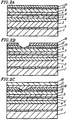
- Reactive ion etching (hereinafter referred to as RIE) is performed in the dry etching apparatus where a pressure is 20 mTorr and an RF power is 150 W while supplying 10 sccm of BCl 3 and 5 sccm of nitrogen. A portion of the n-type current blocking layer 12 corresponding to the opening of the mask 18 is removed, thereby exposing the etch stop layer 17 ( Figure 2B ).
- the substrate structure is brought out of the dry etching apparatus followed by removal of the mask 18 with hydrochloric acid, and then cleaned.
- the substrate structure is put into the MOCVD apparatus again.
- the second p-type cladding layer 11 is formed on the n-type current blocking layer 12 and the etch stop layer 17 by MOCVD, and the p-type contact layer 10 is further formed on the second p-type cladding layer 11 by MOCVD ( Figure 2C ).
- the substrate structure is brought out of the MOCVD apparatus, and then put into the dry etching apparatus again.
- the substrate structure is etched to remove a portion of the primary surface of the p-type contact layer 10 down to the n-type contact layer 3 so that a portion of the upper surface of the n-type contact layer 3 is exposed.
- the p-type electrode 14 is formed on the p-type contact layer 10 by successively depositing nickel and gold
- the n-type electrode 13 is formed on the exposed surface of the n-type contact layer 3 by successively depositing titanium and gold.
- the substrate structure is cleaved to produce an end facet of an oscillator, whereby the semiconductor light-emitting device is completed.
- the etch stop layer 17 that has a high molar fraction of Al in the composition thereof is formed immediately under the n-type current blocking layer 12, resulting in the etching selectivity for dry etching. Therefore, the etching can be substantially stopped at the interface between the n-type current blocking layer 12 and the etch stop layer 17.
- the difference in an Al molar fraction causes the etching selectivity, thereby making it possible to precisely and uniformly control the etching of the n-type current blocking layer 12.
- a gas mixture of BCl 3 and nitrogen is used, so that the uniformity of etching is further improved.
- a nitride-based compound semiconductor device was fabricated, of which a cross-sectional view is shown in Figure 3 .
- the nitride-based compound semiconductor device includes a substrate 1 of sapphire, and further includes a buffer layer 2, a layer 19 of undoped GaN having a thickness of 2 ⁇ m, and a mixed crystal layer 20 of undoped Al x Ga 1-x N having a thickness of 1 ⁇ m, which were successively formed on a substrate 1 by MOCVD.
- the nitride-based compound semiconductor device was put into a dry etching apparatus, and subjected to dry etching by RIE while supplying 10 sccm of BCl 3 and 5 sccm of nitrogen, where a pressure was 20 mTorr and an RF power was 150 W in the dry etching apparatus.
- the substrate 1 may be made of a material other than sapphire, such as, for example, silicon carbide (SiC) and GaN.
- the groove is formed in the n-type current blocking layer 12 by etching.
- the second p-type cladding layer 11 in the shape of a ridge may be formed using a different mask, and the n-type current blocking layer 12 is formed on the sides of the ridge.
- the exemplary embodiment of the present invention provides the semiconductor light-emitting device in which the active layer is formed under the etch stop layer.
- the structure of the device under the etch stop layer can be modified in such a way to fabricate semiconductor devices (e.g., a transistor) other than the semiconductor light-emitting device.
Landscapes
- Physics & Mathematics (AREA)
- Condensed Matter Physics & Semiconductors (AREA)
- General Physics & Mathematics (AREA)
- Electromagnetism (AREA)
- Optics & Photonics (AREA)
- Semiconductor Lasers (AREA)
- Drying Of Semiconductors (AREA)
- Junction Field-Effect Transistors (AREA)
- Led Devices (AREA)
Applications Claiming Priority (2)
| Application Number | Priority Date | Filing Date | Title |
|---|---|---|---|
| JP30357598 | 1998-10-26 | ||
| JP30357598 | 1998-10-26 |
Publications (3)
| Publication Number | Publication Date |
|---|---|
| EP0997996A2 true EP0997996A2 (fr) | 2000-05-03 |
| EP0997996A3 EP0997996A3 (fr) | 2000-11-08 |
| EP0997996B1 EP0997996B1 (fr) | 2006-11-22 |
Family
ID=17922661
Family Applications (1)
| Application Number | Title | Priority Date | Filing Date |
|---|---|---|---|
| EP99120838A Expired - Lifetime EP0997996B1 (fr) | 1998-10-26 | 1999-10-25 | Dispositif laser à semi-conducteur et procédé de fabrication |
Country Status (6)
| Country | Link |
|---|---|
| US (1) | US6503769B2 (fr) |
| EP (1) | EP0997996B1 (fr) |
| JP (1) | JP2000200946A (fr) |
| KR (1) | KR100653567B1 (fr) |
| DE (1) | DE69934075T2 (fr) |
| TW (1) | TW439336B (fr) |
Families Citing this family (13)
| Publication number | Priority date | Publication date | Assignee | Title |
|---|---|---|---|---|
| KR100361593B1 (ko) * | 2000-11-23 | 2002-11-22 | 주식회사일진 | 볼록 요철을 갖는 광학집적회로 소자, 그 제조방법, 그광학집적 회로 소자를 이용하여 제조한 광통신용 송수신장치의 모듈 |
| US6709881B2 (en) * | 2000-11-28 | 2004-03-23 | Matsushita Electric Industrial Co., Ltd. | Method for manufacturing semiconductor and method for manufacturing semiconductor device |
| JP3464991B2 (ja) | 2000-11-28 | 2003-11-10 | 松下電器産業株式会社 | 半導体レーザ発光装置の製造方法 |
| JP3454791B2 (ja) * | 2001-03-01 | 2003-10-06 | 三洋電機株式会社 | 窒化物系半導体素子および窒化物系半導体の形成方法 |
| JP3956941B2 (ja) * | 2001-06-15 | 2007-08-08 | 日亜化学工業株式会社 | 窒化物半導体発光素子及びそれを用いた発光装置 |
| US20050079642A1 (en) * | 2003-10-14 | 2005-04-14 | Matsushita Elec. Ind. Co. Ltd. | Manufacturing method of nitride semiconductor device |
| US20050274964A1 (en) * | 2004-05-29 | 2005-12-15 | Ting-Kai Huang | Light emitting diode structure |
| US7320898B2 (en) * | 2004-06-17 | 2008-01-22 | Matsushita Electric Industrial Co., Ltd. | Semiconductor laser device and method for fabricating the same |
| US7508001B2 (en) | 2004-06-21 | 2009-03-24 | Panasonic Corporation | Semiconductor laser device and manufacturing method thereof |
| JP2007042944A (ja) * | 2005-08-04 | 2007-02-15 | Rohm Co Ltd | 窒化物半導体素子の製法 |
| JP5298938B2 (ja) * | 2009-02-24 | 2013-09-25 | 住友電気工業株式会社 | 半導体素子の製造方法 |
| JP2015005534A (ja) * | 2013-06-18 | 2015-01-08 | 学校法人立命館 | 縦型発光ダイオードおよび結晶成長方法 |
| US20180061975A1 (en) * | 2016-08-24 | 2018-03-01 | Rohm Co., Ltd. | Nitride semiconductor device and nitride semiconductor package |
Family Cites Families (9)
| Publication number | Priority date | Publication date | Assignee | Title |
|---|---|---|---|---|
| JPH0619801A (ja) | 1992-07-02 | 1994-01-28 | Hitachi Ltd | 情報処理装置 |
| US5646953A (en) * | 1994-04-06 | 1997-07-08 | Matsushita Electronics Corporation | Semiconductor laser device |
| US5650641A (en) * | 1994-09-01 | 1997-07-22 | Toyoda Gosei Co., Ltd. | Semiconductor device having group III nitride compound and enabling control of emission color, and flat display comprising such device |
| JPH09232681A (ja) | 1996-02-22 | 1997-09-05 | Hitachi Ltd | 窒化物系化合物半導体光素子 |
| US5970080A (en) | 1996-03-07 | 1999-10-19 | Sharp Kabushiki Kaisha | Gallium nitride compound semiconductor light emitting element and method for fabricating the same |
| JP3713100B2 (ja) | 1996-05-23 | 2005-11-02 | ローム株式会社 | 半導体発光素子の製法 |
| US5834379A (en) * | 1996-07-16 | 1998-11-10 | Cornell Research Foundation, Inc. | Process for synthesis of cubic GaN on GaAs using NH3 in an RF plasma process |
| JP3787195B2 (ja) * | 1996-09-06 | 2006-06-21 | シャープ株式会社 | 窒化ガリウム系化合物半導体発光素子の製造方法 |
| US5923946A (en) * | 1997-04-17 | 1999-07-13 | Cree Research, Inc. | Recovery of surface-ready silicon carbide substrates |
-
1999
- 1999-10-20 US US09/420,722 patent/US6503769B2/en not_active Expired - Lifetime
- 1999-10-22 JP JP30171299A patent/JP2000200946A/ja active Pending
- 1999-10-25 DE DE69934075T patent/DE69934075T2/de not_active Expired - Lifetime
- 1999-10-25 EP EP99120838A patent/EP0997996B1/fr not_active Expired - Lifetime
- 1999-10-26 TW TW088118472A patent/TW439336B/zh not_active IP Right Cessation
- 1999-10-26 KR KR1019990046566A patent/KR100653567B1/ko not_active Expired - Fee Related
Also Published As
| Publication number | Publication date |
|---|---|
| KR20000029321A (ko) | 2000-05-25 |
| KR100653567B1 (ko) | 2006-12-05 |
| JP2000200946A (ja) | 2000-07-18 |
| US20020167018A1 (en) | 2002-11-14 |
| EP0997996B1 (fr) | 2006-11-22 |
| TW439336B (en) | 2001-06-07 |
| DE69934075T2 (de) | 2007-04-05 |
| EP0997996A3 (fr) | 2000-11-08 |
| DE69934075D1 (de) | 2007-01-04 |
| US6503769B2 (en) | 2003-01-07 |
Similar Documents
| Publication | Publication Date | Title |
|---|---|---|
| KR100917260B1 (ko) | 결정막, 결정기판 및 반도체장치 | |
| US6911351B2 (en) | Method of fabricating nitride semiconductor, method of fabricating nitride semiconductor device, nitride semiconductor device, semiconductor light emitting device and method of fabricating the same | |
| US7026182B2 (en) | Semiconductor device, semiconductor laser, their manufacturing methods and etching methods | |
| US5981977A (en) | Nitride compound semiconductor light emitting element and its manufacturing method | |
| KR100303963B1 (ko) | 질화갈륨계화합물반도체발광소자및그제조방법 | |
| KR20010052808A (ko) | 반도체 레이저, 반도체 장치 및 그의 제조 방법 | |
| US6503769B2 (en) | Semiconductor device and method for fabricating the same | |
| US20010025989A1 (en) | Semiconductor device and method of manufacturing the same | |
| JP2003332688A (ja) | Iii族窒化物系化合物半導体レーザ | |
| US6977186B2 (en) | Method for manufacturing semiconductor laser optical device | |
| EP1291904A2 (fr) | Substrat de GaN formé sur une couche de GaN présentant des trous minces discrets réalisés par croissance sélective | |
| JP2007019492A (ja) | 単一のステップmocvdによって製造される導波格子を組み込んだ埋め込みヘテロ構造デバイス | |
| WO2009141933A1 (fr) | Laser semi-conducteur à base de nitrure | |
| JPH09283861A (ja) | 3族窒化物半導体レーザダイオードの製造方法 | |
| JP5027647B2 (ja) | 単一のステップmocvdによって製造される埋め込みヘテロ構造デバイス | |
| EP1553669A1 (fr) | Dispositif electroluminescent semi-conducteur au nitrure du groupe iii et procede permettant de produire ce dispositif | |
| KR20000035669A (ko) | 반도체 레이저, 반도체 장치 및 이들의 제조 방법 | |
| JP2001007443A (ja) | 半導体発光装置の製造方法 | |
| KR20000077066A (ko) | 반도체 레이저, 그 제조 방법, 반도체 장치 및 그 제조 방법 | |
| JP3464991B2 (ja) | 半導体レーザ発光装置の製造方法 | |
| JP4623799B2 (ja) | 半導体発光素子の製法および半導体レーザ | |
| JP4415440B2 (ja) | 半導体レーザの製造方法 | |
| JP4741055B2 (ja) | 半導体発光素子 | |
| JP4826019B2 (ja) | 半導体レーザ素子の製造方法 | |
| JP2004055881A (ja) | 光半導体装置の製造方法 |
Legal Events
| Date | Code | Title | Description |
|---|---|---|---|
| PUAI | Public reference made under article 153(3) epc to a published international application that has entered the european phase |
Free format text: ORIGINAL CODE: 0009012 |
|
| AK | Designated contracting states |
Kind code of ref document: A2 Designated state(s): DE FR GB |
|
| AX | Request for extension of the european patent |
Free format text: AL;LT;LV;MK;RO;SI |
|
| PUAL | Search report despatched |
Free format text: ORIGINAL CODE: 0009013 |
|
| AK | Designated contracting states |
Kind code of ref document: A3 Designated state(s): AT BE CH CY DE DK ES FI FR GB GR IE IT LI LU MC NL PT SE |
|
| AX | Request for extension of the european patent |
Free format text: AL;LT;LV;MK;RO;SI |
|
| 17P | Request for examination filed |
Effective date: 20010131 |
|
| AKX | Designation fees paid |
Free format text: DE FR GB |
|
| RAP1 | Party data changed (applicant data changed or rights of an application transferred) |
Owner name: MATSUSHITA ELECTRIC INDUSTRIAL CO., LTD. |
|
| RAP1 | Party data changed (applicant data changed or rights of an application transferred) |
Owner name: MATSUSHITA ELECTRIC INDUSTRIAL CO., LTD. |
|
| 17Q | First examination report despatched |
Effective date: 20050606 |
|
| GRAP | Despatch of communication of intention to grant a patent |
Free format text: ORIGINAL CODE: EPIDOSNIGR1 |
|
| RIC1 | Information provided on ipc code assigned before grant |
Ipc: H01S 5/323 20060101AFI20060424BHEP |
|
| RTI1 | Title (correction) |
Free format text: SEMICONDUCTOR LASER DEVICE AND METHOD FOR FABRICATING THE SAME |
|
| GRAS | Grant fee paid |
Free format text: ORIGINAL CODE: EPIDOSNIGR3 |
|
| GRAA | (expected) grant |
Free format text: ORIGINAL CODE: 0009210 |
|
| AK | Designated contracting states |
Kind code of ref document: B1 Designated state(s): DE FR GB |
|
| REG | Reference to a national code |
Ref country code: GB Ref legal event code: FG4D |
|
| REF | Corresponds to: |
Ref document number: 69934075 Country of ref document: DE Date of ref document: 20070104 Kind code of ref document: P |
|
| ET | Fr: translation filed | ||
| PLBE | No opposition filed within time limit |
Free format text: ORIGINAL CODE: 0009261 |
|
| STAA | Information on the status of an ep patent application or granted ep patent |
Free format text: STATUS: NO OPPOSITION FILED WITHIN TIME LIMIT |
|
| 26N | No opposition filed |
Effective date: 20070823 |
|
| PGFP | Annual fee paid to national office [announced via postgrant information from national office to epo] |
Ref country code: GB Payment date: 20131023 Year of fee payment: 15 |
|
| PGFP | Annual fee paid to national office [announced via postgrant information from national office to epo] |
Ref country code: FR Payment date: 20141008 Year of fee payment: 16 Ref country code: DE Payment date: 20141023 Year of fee payment: 16 |
|
| GBPC | Gb: european patent ceased through non-payment of renewal fee |
Effective date: 20141025 |
|
| PG25 | Lapsed in a contracting state [announced via postgrant information from national office to epo] |
Ref country code: GB Free format text: LAPSE BECAUSE OF NON-PAYMENT OF DUE FEES Effective date: 20141025 |
|
| REG | Reference to a national code |
Ref country code: DE Ref legal event code: R119 Ref document number: 69934075 Country of ref document: DE |
|
| PG25 | Lapsed in a contracting state [announced via postgrant information from national office to epo] |
Ref country code: DE Free format text: LAPSE BECAUSE OF NON-PAYMENT OF DUE FEES Effective date: 20160503 |
|
| REG | Reference to a national code |
Ref country code: FR Ref legal event code: ST Effective date: 20160630 |
|
| PG25 | Lapsed in a contracting state [announced via postgrant information from national office to epo] |
Ref country code: FR Free format text: LAPSE BECAUSE OF NON-PAYMENT OF DUE FEES Effective date: 20151102 |