EP0998004A1 - Procede de prevention des surcharges, circuit chargeur, dispositif electronique et compteur de temps - Google Patents
Procede de prevention des surcharges, circuit chargeur, dispositif electronique et compteur de temps Download PDFInfo
- Publication number
- EP0998004A1 EP0998004A1 EP99909251A EP99909251A EP0998004A1 EP 0998004 A1 EP0998004 A1 EP 0998004A1 EP 99909251 A EP99909251 A EP 99909251A EP 99909251 A EP99909251 A EP 99909251A EP 0998004 A1 EP0998004 A1 EP 0998004A1
- Authority
- EP
- European Patent Office
- Prior art keywords
- charging
- voltage
- power supply
- input terminal
- supply line
- Prior art date
- Legal status (The legal status is an assumption and is not a legal conclusion. Google has not performed a legal analysis and makes no representation as to the accuracy of the status listed.)
- Granted
Links
Images







Classifications
-
- H—ELECTRICITY
- H02—GENERATION; CONVERSION OR DISTRIBUTION OF ELECTRIC POWER
- H02J—ELECTRIC POWER NETWORKS; CIRCUIT ARRANGEMENTS OR SYSTEMS FOR SUPPLYING OR DISTRIBUTING ELECTRIC POWER; SYSTEMS FOR STORING ELECTRIC ENERGY
- H02J7/00—Circuit arrangements for charging or discharging batteries or for supplying loads from batteries
- H02J7/02—Circuit arrangements for charging or discharging batteries or for supplying loads from batteries for charging batteries from AC mains by converters
-
- H—ELECTRICITY
- H02—GENERATION; CONVERSION OR DISTRIBUTION OF ELECTRIC POWER
- H02J—ELECTRIC POWER NETWORKS; CIRCUIT ARRANGEMENTS OR SYSTEMS FOR SUPPLYING OR DISTRIBUTING ELECTRIC POWER; SYSTEMS FOR STORING ELECTRIC ENERGY
- H02J7/00—Circuit arrangements for charging or discharging batteries or for supplying loads from batteries
- H02J7/60—Circuit arrangements for charging or discharging batteries or for supplying loads from batteries including safety or protection arrangements
- H02J7/61—Circuit arrangements for charging or discharging batteries or for supplying loads from batteries including safety or protection arrangements against overcharge
-
- H—ELECTRICITY
- H02—GENERATION; CONVERSION OR DISTRIBUTION OF ELECTRIC POWER
- H02J—ELECTRIC POWER NETWORKS; CIRCUIT ARRANGEMENTS OR SYSTEMS FOR SUPPLYING OR DISTRIBUTING ELECTRIC POWER; SYSTEMS FOR STORING ELECTRIC ENERGY
- H02J7/00—Circuit arrangements for charging or discharging batteries or for supplying loads from batteries
- H02J7/60—Circuit arrangements for charging or discharging batteries or for supplying loads from batteries including safety or protection arrangements
- H02J7/64—Circuit arrangements for charging or discharging batteries or for supplying loads from batteries including safety or protection arrangements against overvoltage
-
- H—ELECTRICITY
- H02—GENERATION; CONVERSION OR DISTRIBUTION OF ELECTRIC POWER
- H02J—ELECTRIC POWER NETWORKS; CIRCUIT ARRANGEMENTS OR SYSTEMS FOR SUPPLYING OR DISTRIBUTING ELECTRIC POWER; SYSTEMS FOR STORING ELECTRIC ENERGY
- H02J7/00—Circuit arrangements for charging or discharging batteries or for supplying loads from batteries
- H02J7/80—Circuit arrangements for charging or discharging batteries or for supplying loads from batteries including monitoring or indicating arrangements
Definitions
- the present invention relates to an overcharge prevention method, which is suitable for preventing overcharging, a charging circuit, electronic equipment which uses the overcharge prevention method and the charging circuit, and a timepiece.
- a diode bridge circuit is well known as a charging circuit that charges a large-capacity capacitor with an alternating voltage generated by a generator. In the diode bridge circuit, since losses for only two diode voltage drops are generated, it is not suitable for charging small amplitude alternating voltage.
- FIG. 15 is a circuit diagram of a conventional charging circuit.
- this charging circuit there are provided comparators COM1 and COM2 for comparing the voltages at output terminals A and B, respectively, of a generator AG with the power supply voltage Vdd, comparators COM3 and COM4 for comparing the voltages at the output terminals A and B, respectively, of the generator AG with the ground voltage GND, and a large-capacity capacitor C for storing a charging current. Then, switching ON/OFF of P-channel FETs P1 and P2 and N-channel FETs N1 and N2 is controlled according to the outputs of the respective comparators COM1 to COM4.
- the N-channel FET N1 is turned ON by the comparator COM3, and the output terminal A is grounded. Further, when the voltage of the output terminal B exceeds the power supply voltage Vdd, the P-channel FET P2 is turned ON by the comparator COM2, and electrical charge flows into the capacitor C through a path indicated with the arrow. In this case, unless the voltage of the output terminal B exceeds the power supply voltage Vdd, the P-channel FET P2 will not turn ON, and it is arranged to prevent any problems from occurring such as a current flowing through a path opposite to the arrow, thereby deteriorating the charging efficiency.
- the present invention is characterized in that an overcharge prevention method, which is adapted to be used in a charging circuit for charging electrical power into a charging element, using a rectifying circuit having a plurality of rectifying elements, which converts an alternating-current input from an external alternating-current power supply through a pair of input terminals to a direct-current and outputs the direct-current, characterized in that the method comprises the steps of detecting a charging voltage of the charging element; and shunting the pair of input terminals without passing through the plurality of rectifying elements when the detected charging voltage exceeds a predetermined voltage that is defined in advance.
- an overcharge prevention method which is adapted to be used in a charging circuit for charging electrical power into a charging element, using a rectifying circuit having a plurality of rectifying elements, which converts an alternating current input from an external alternating-current power supply through a pair of input terminals to a direct current and outputs the direct current
- the method comprises the steps of detecting a charging voltage of the charging element; comparing the detected charging voltage with a reference voltage that is defined in advance; and shunting the pair of input terminals without passing through the plurality of rectifying elements when the detected charging voltage exceeds the reference voltage.
- the present invention is characterized in that an overcharge prevention method which is used in a charging circuit, the charging circuit comprising first and second switching means with which it is controlled whether or not, according to a terminal voltage at one of the input terminals to which an alternating-current voltage is supplied, the other one of the input terminals and a first power supply line are connected, first and second diodes which are connected between the respective input terminals and a second power supply line, and a charging element for rectifying the alternating-current voltage and for charging electrical power into the charging element, characterized in that the method comprises the steps of detecting a charging voltage of the charging element; comparing the detected charging voltage with a reference voltage that is defined in advance; and supplying a generator current that flows into one of the input terminals to the other one of the input terminals through a path that does not pass through the first and second diodes when the detected charging voltage exceeds the reference voltage.
- the present invention is characterized in that a generator current that flows into one of the input terminals is supplied to the other one of the input terminals through a path that does not pass through the first and second diodes by shunting both of the input terminals, when the detected charging voltage exceeds the reference voltage.
- the present invention is characterized in that a charging circuit for charging electrical power into a charging element, using a rectifying circuit having a plurality of rectifying elements, which converts an alternating-current input from an external alternating-current power supply through a pair of input terminals to a direct current and outputs the direct current, characterized in that the charging circuit comprises charging voltage detecting means for detecting a charging voltage of the charging element; and shunt means for shunting the pair of input terminals without passing through the plurality of rectifying elements when the detected charging voltage exceeds a predetermined voltage that is defined in advance.
- the present invention is characterized in that a charging circuit for charging electrical power into a charging element, using a rectifying circuit having a plurality of rectifying elements, which converts an alternating current input from an external alternating-current power supply through a pair of input terminals to a direct current and outputs the direct current, characterized in that the charging circuit comprises charging voltage detecting means for detecting a charging voltage of the charging element; comparison means for comparing the detected charging voltage with a reference voltage that is defined in advance; and shunt means for shunting the pair of input terminals without passing through the plurality of rectifying elements when the detected charging voltage exceeds the reference voltage.
- the present invention is further characterized in that a charging circuit for rectifying an alternating-current voltage supplied to first and second input terminals and for charging an electrical charge into a charging element that is provided between first and second power supply lines, comprising first switching means provided between the first input terminal and the first power supply line, in which ON/OFF switching thereof is controlled on the basis of a voltage at the second input terminal; second switching means provided between the second input terminal and the first power supply line, in which ON/OFF switching thereof is controlled on a basis of a voltage at the first input terminal; a first diode provided between the first input terminal and the second power supply line; a second diode provided between the second input terminal and the second power supply line; comparison means for detecting a charging voltage of the charging element, and for comparing the detected charging voltage with a reference voltage that is defined in advance; and shunt means for shunting the first input terminal and the second input terminal by supplying a generator current that flows into one of the input terminals to the other one of the input terminals through a path that does not pass
- the present invention is characterized in that the shunt means is a transistor provided between the first input terminal and the second input terminal.
- the shunt means comprises a third diode in which one end thereof is connected to the first input terminal; a fourth diode in which one end thereof is connected to the second input terminal; and a transistor which is connected to the other ends of the third and fourth diodes and is also connected to the first and second power source lines.
- the present invention is further characterized in that a charging circuit for rectifying an alternating-current voltage supplied to first and second input terminals and for charging electrical power into a charging element that is provided between a high-potential power supply line and a low-potential power supply line, comprising a first diode in which an anode thereof is connected to the first input terminal, and a cathode thereof is connected to the high-potential power supply line; a second diode in which an anode thereof is connected to the second input terminal, and a cathode thereof is connected to the high-potential power supply line; a first N-channel field effect transistor in which a drain thereof is connected to the first input terminal, a source thereof is connected to the low-potential power supply line, and a gate thereof is connected to the second input terminal; a second N-channel field effect transistor in which a drain thereof is connected to the second input terminal, a source thereof is connected to the low-potential power supply line, and a gate thereof is connected to the first input terminal; a
- the present invention is further characterized in that a charging circuit for rectifying an alternating-current voltage supplied to first and second input terminals and for charging electrical power into a charging element that is provided between a high-potential power supply line and a low-potential power supply line, comprising a first diode in which a cathode thereof is connected to the first input terminal, and an anode thereof is connected to the low-potential power supply line; a second diode in which a cathode thereof is connected to the second input terminal, and an anode thereof is connected to the low-potential power supply line; a first P-channel field effect transistor in which a drain thereof is connected to the first input terminal, a source thereof is connected to the high-potential power supply line, and a gate thereof is connected to the second input terminal; a second P-channel field effect transistor in which a drain thereof is connected to the second input terminal, a source thereof is connected to the high-potential power supply line, and a gate thereof is connected to the first input terminal; a
- a charging circuit for rectifying an alternating-current voltage supplied to first and second input terminals and for charging electrical power into a charging element that is provided between a high-potential power supply line and a low-potential power supply line, comprising a first diode in which an anode thereof is connected to the first input terminal, and a cathode thereof is connected to the high-potential power supply line; a second diode in which an anode thereof is connected to the second input terminal, and a cathode thereof is connected to the high-potential power supply line; a first N-channel field effect transistor in which a drain thereof is connected to the first input terminal, a source thereof is connected to the low-potential power supply line, and a gate thereof is connected to the second input terminal; a second N-channel field effect transistor in which a drain thereof is connected to the second input terminal, a source thereof is connected to the low-potential power supply line, and a gate thereof is connected to the first input terminal; a
- the present invention is characterized in that a charging circuit for rectifying an alternating-current voltage supplied to first and second input terminals and for charging electrical power into a charging element that is provided between a high-potential power supply line and a low-potential power supply line, comprising a first diode in which a cathode thereof is connected to the first input terminal, and an anode thereof is connected to the low-potential power supply line; a second diode in which a cathode thereof is connected to the second input terminal, and an anode thereof is connected to the low-potential power supply line; a first P-channel field effect transistor in which a drain thereof is connected to the first input terminal, a source thereof is connected to the high-potential power supply line, and a gate thereof is connected to the second input terminal; a second P-channel field effect transistor in which a drain thereof is connected to the second input terminal, a source thereof is connected to the high-potential power supply line, and a gate thereof is connected to the first input terminal;
- the present invention is further characterized in that a charging circuit for rectifying an alternating-current voltage supplied to first and second input terminals and for charging electrical power into a charging element that is provided between a high-potential power supply line and a low-potential power supply line, comprising a first diode in which an anode thereof is connected to the first input terminal, and a cathode thereof is connected to the high-potential power supply line; a second diode in which an anode thereof is connected to the second input terminal, and a cathode thereof is connected to the high-potential power supply line; a first N-channel field effect transistor in which a drain thereof is connected to the first input terminal, a source thereof is connected to the low-potential power supply line, and a gate thereof is connected to the second input terminal; a second N-channel field effect transistor in which a drain thereof is connected to the second input terminal, a source thereof is connected to the low-potential power supply line, and a gate thereof is connected to the first input terminal; a
- An electronic equipment of the present invention is characterized in that there is installed a charging circuit according to the respective embodiments described above and operates in accordance with electrical power that is supplied from the charging circuit.
- a timepiece of the present invention is characterized in that there is installed a charging circuit according to the respective embodiments described above and includes a clock circuit that measures time in accordance with electrical power that is supplied from the charging circuit.
- Fig. 1 is a diagram for illustrating the principle of a charging circuit that is used in a wristwatch according to a first embodiment.
- the main part of the charging circuit 100 is comprised of a rectification unit 10 for rectifying a generated voltage of an AC generator AG, a large-capacity capacitor 20 for storing a charging current, a voltage-detection determination unit 30A for detecting a charging voltage Va of the large-capacity capacitor 20 and for outputting a control signal CS to control whether or not input terminals AG1 and AG2 are shunted based on the detected charging voltage Va, and a shunt unit 40 for shunting the input terminals AG1 and AG2 based on the detection result.
- d shown in the figure denotes a parasitic diode.
- the voltage-detection determination unit 30A is arranged such that the control signal CS for shunting the input terminals AG1 and AG2 is output when the charging voltage Va exceeds a predetermined voltage, or it is arranged such that it determines whether or not the charging voltage Va exceeds the predetermined voltage, and the control signal CS for shunting the input terminals AG1 and AG2 is output if it determines that exceeding occurs.
- the shunt unit 40 operates, and the input terminals AG1 and AG2 are shunted, and, for example, when the terminal voltage AG1 (V1) increases and the terminal voltage AG2 (V2) decreases, a limiter current ILIM flows through the path indicated by an arrow X in the figure.
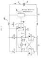
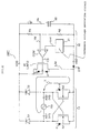
- Fig. 2 is a circuit diagram of a charging circuit that is used in a wristwatch according to the first embodiment.
- d shown in the figure denotes a parasitic diode.
- the rectification unit 10 is configured as a bridge-type full-wave rectifying circuit, and is arranged such that the generator voltage of the AC generator AG is supplied to the input terminals AG1 and AG2.
- the input terminals AG1 and AG2 are connected to the anodes of diodes D1 and D2, respectively, in which the cathodes thereof are connected to a high-potential power supply line VDD.
- the diodes D1 and D2 turn ON when the terminal voltages V1 and V2 of the input terminals AG1 and AG2 exceed the total values of the charging voltage Va and the voltage drop Vf of the diodes D1 and D2.
- enhancement-type N-channel FETs N1 and N2 are provided between the input terminals AG1 and AG2 and a low-potential power supply line VSS.
- a gate of the N-channel FET N1 is connected to the input terminal AG2, while a gate of the N-channel FET N2 is connected to the input terminal AG1.
- the N-channel FETs N1 and N2 have identical electrical characteristics, and the threshold voltages thereof are Vt.
- the N-channel FET N1 turns ON. At this moment, the N-channel FET N2 is OFF. Further, if the amplitude of the generator voltage is extremely small, the diode D2 should be OFF. If the generated voltage increases gradually, and the terminal voltage V2 exceeds the total value of the charging voltage Va and the voltage drop Vf of the diode D2, the diode D2 turns ON.
- the charging current i flows through the path: "the input terminal AG2 ⁇ the diode D2 ⁇ the high-potential power supply line VDD ⁇ the large-capacity capacitor 20 ⁇ the low-potential power supply line VSS ⁇ the N-channel FET N1 ⁇ the input terminal AG1", and the electrical charge changes the large-capacity capacitor 20.
- the charging current i flows through the path: "the input terminal AG1 ⁇ the diode D1 ⁇ the high-potential power supply line VDD ⁇ the large-capacity capacitor 20 ⁇ the low-potential power supply line VSS ⁇ the N-channel FET N2 ⁇ the input terminal AG2", and the electrical charge charges the large-capacity capacitor 20.
- This rectification unit 10 has an advantage that the circuit size of the charging circuit is small because it does not require the comparators COM1 to COM4, as in the conventional charging circuit shown in Fig. 15, and also it has an advantage that it can charge efficiently even if the amplitude of the generator voltage is small because the voltage loss is smaller compared with the diode bridge circuit.
- the large-capacity capacitor 20 is composed of, for example, a chargeable secondary battery, and has a certain breakdown voltage. If charging is performed to exceed the breakdown voltage, overcharging occurs, and the large-capacity capacitor 20 deteriorates, and thereby the charging efficiency degrades.
- the comparator 30 is comprised of a comparator COM, resistors R1 and R2 that divide the charging voltage Va, and a reference-voltage generation circuit 31 that generates a reference voltage Vref.
- the comparator COM compares the reference voltage Vref and the voltage Va', and generates a control signal CS.
- the control signal CS becomes low, and on the other hand, if the voltage Va' is less than the reference Vref, the control signal CS becomes high.
- the reference Vref is set such that the large-capacity capacitor 20 is not overcharged, by considering the breakdown voltage of the large-capacity capacitor 20. Further, the reason why it is arranged to compare the charging voltage Va with the voltage Va', but not to compare it directly with the reference voltage Vref, is that the ease of producing the reference voltage Vref is considered.
- the shunt unit 40 is composed of a limiter transistor LIMTr.
- the limiter transistor LIMTr a P-channel enhancement-type transmission gate transistor is used, and it is connected to the input terminals AG1 and AG2. Switching ON/OFF of the transmission gate transistor is controlled by a gate voltage thereof, and has bi-directionality of input/output.
- the control signal CS since it is comprised of a P-channel, it turns ON (connected) when the control signal CS is in a low level, and turns OFF (open) when the control signal CS is in a high level. Accordingly, if the charging voltage Va exceeds a predetermined voltage, the input terminals AG1 and AG2 are connected, and a limiter current ILIM flows, so as to prevent the charging current i from flowing into the large-capacity capacitor 20.
- FIG. 3 is a perspective view showing the configurations of the AC generator AG and the peripheral mechanism thereof.
- the AC generator AG is provided with a rotor 14 and a stator 15, and it is arranged that an electromotive force is generated in an outputting coil 16 of the stator 15 when the dipole-magnetized disk shaped rotor 14 rotates, thereby an AC output can be extracted.
- the numeral 13 denotes a revolving weight that performs a rotational movement within a wristwatch body case
- the numeral 11 denotes a wheel array mechanism that transmits the rotational movement of the revolving weight 13 to the AC generator AG.
- the revolving weight 13 is arranged such that it rotates in response to the swing of a person's arm who wears the wristwatch, thereby enabling an electromotive force to be obtained from the AC generator AG.
- An AC (alternating current) that is output from the AC generator AG is rectified in the charging circuit 100, and is supplied to a processing device 9.
- the processing device 9 drives a watch device 7 by the electrical power that is discharged from the charging circuit 100. Further, even when the AC generator AG is in a non-generating state, the processing device 9 and the watch device 7 are driven by the electrical power supplied from the large-capacity capacitor 20.
- This watch device 7 is comprised of a crystal oscillator, a counter circuit and the like, and is arranged such that a master clock signal generated in the crystal oscillator is frequency divided in the counter circuit, and time is measured on a basis of this frequency-divided result.
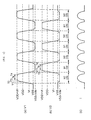
- Fig. 4 is a timing chart showing a charging operation of the charging circuit.
- the generator voltage is supplied to both of the input terminals AG1 and AG2.
- the terminal voltage V1 at the input terminal AG1 and the terminal voltage V2 at the input terminal AG2 are such that the phases thereof are reversed, as shown in Figs. 4(a) and 4(b).
- Vt in the figure denotes a threshold voltage of the N-channel FETs N1 and N2.
- the N-channel FET N2 turns ON. Thereafter, the terminal voltage V1 rises, and then exceeds the voltage of the high-potential power supply line VDD at time T2, and further, when it rises by an amount of the voltage drop Vf of the diode D1 (at time T3), the diode D1 turns ON. At this moment, since the terminal voltage V2 is below the threshold voltage Vt, the N-channel FET N1 is turned OFF.
- the charging current i flows through the path: "the input terminal AG1 ⁇ the diode D1 ⁇ the high-potential power supply line VDD ⁇ the large-capacity capacitor 20 ⁇ the low-potential power supply line VSS ⁇ the N-channel FET N2", and the electric charge charges the large-capacity capacitor 20.
- the terminal voltage V2 rises when the terminal voltage V1 falls, and the terminal voltage V2 exceeds the threshold voltage Vt at time T5. Then, the N-channel FET N1 turns ON. Thereafter, the terminal voltage V2 rises and exceeds the high-potential power supply line VDD at time T6, and further when it rises by an amount of the voltage drop Vf of the diode D2 (at time T7), the diode D2 turns ON. At this moment, since the terminal voltage V1 is below the threshold voltage Vt, the N-channel FET N2 turns OFF.
- the charging current i flows through the path: "the input terminal AG2 ⁇ the diode D2 ⁇ the high-potential power supply line VDD ⁇ the large-capacity capacitor 20 ⁇ the low-potential power supply line VSS ⁇ the N-channel FET N1", and the electric charge charges the large-capacity capacitor 20.
- the generator voltage is full-wave rectified, and thus the charging current i shown in Fig. 4(c) is obtained.
- step S2 because the limiter transistor LIMTr switches from OFF to ON (step S2), the input terminals AG1 and AG2 are shunted, and, for example, when the terminal voltage AG1 (V1) rises and the terminal voltage AG2 (V2) falls, the limiter current ILIM flows through the path as indicated by an arrow X in the figure.
- Overvoltage detection is a detection operation which may be performed by sampling even when the detection is not constantly performed. More concretely, the comparator COM and the resistors R1 and R2 are configured such that the power supplies thereto are stopped with a transistor switch, and the power is supplied to the comparator COM and the resistors R1 and R2 by turning the transistor switch ON for a period of a few seconds, and the overvoltage detection is performed, thereby reducing the current consumed according to the detection operation.
- a latch circuit may preferably be provided at an output of the comparator in order to maintain the output signal of the comparator during the sampling period.
- this charging circuit 100 has a self-control characteristic such that the limiter current ILIM is reduced by forming a path for shunting.
- the limiter transistor LIMTr is provided between the rectification unit 10 and the large-capacity capacitor 20, and the rectification unit 10 and the large-capacity capacitor 20 are disconnected by turning the limiter transistor LIMTr OFF when the charging voltage Va exceeds a predetermined voltage.
- the circuit scale can be made small, and also the current consumed can be reduced.
- the shunt unit 40 is configured using a transmission gate, and is controlled so that the transmission gate is turned ON when the charging voltage Va' that is divided from the charging voltage Va exceeds the reference voltage Vref, the charging voltage Va will never exceed the breakdown voltage of the large-capacity capacitor 20, thereby enabling the prevention of overcharging of the large-capacity capacitor 20.
- the shunt unit 40 is arranged to flow the generator current through a path that will not go through the diodes D1 and D2, but not by disconnecting the rectification unit 10 and the large-capacity capacitor 20, a transistor with a low breakdown voltage can be used for the one that is utilized in the shunt unit 40, thereby it is easily made as an IC. Further, when shunting the input terminals AG1 and AG2, a short brake is applied, so that the amplitudes of the terminal voltages V1 and V2 can be automatically lowered.
- a source potential of the limiter transistor LIMTr rises above a body potential by an amount of the voltage drop Vf of the diodes D1 and D2 at the time of electricity generation
- the threshold voltage Vt of the limiter transistor is reduced due to a backgate effect.
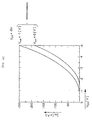
- Fig. 16 shows the IDS-VGS characteristics of an enhancement-type P-channel FET, which is commonly used. From this figure, it is apparent that the IDS-VGS characteristic varies when the body potential Vsub is reduced for the source potential Vs, and thus the threshold voltage Vt (absolute value between the gate and the source) is lowered.
- the charging voltage Va does not reach a predetermined voltage, and thus there is a case in which a small limiter current ILIM flows, as a resistance value between the source and the gate of the limiter transistor LIMTr is decreased during a period of time in which the limiter transistor LIMTr should be primarily OFF.
- a small limiter current ILIM flows, as a resistance value between the source and the gate of the limiter transistor LIMTr is decreased during a period of time in which the limiter transistor LIMTr should be primarily OFF.
- the generator current is large and the voltage drop Vf becomes large.
- the threshold voltage Vt of the MOSFET is set to a low voltage such as 0.5 V, the influence of the backgate effect is substantial.
- the second embodiment is made, and when the charging voltage Va does not reach the reference voltage Vref, a shunt path of the input terminals AG1 and AG2 is securely opened.
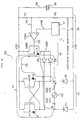
- Fig. 6 is a circuit diagram of a charging circuit that is used in a wristwatch according to the second embodiment.
- the charging circuit 101 is configured similarly to the charging circuit 100 of the first embodiment shown in Fig. 2, except for the points that instead of the rectification unit 10 of the first embodiment, a rectification unit 10' in which the low-potential power supply line VSS and the high-potential power supply line VDD are reversed is used, and a shunt unit 40' is used.
- the configurations of the AC generator AG and the peripheral mechanism thereof are similar to the ones of the first embodiment shown in Fig. 3.
- the input terminals AG1 and AG2 are connected to the low-potential power supply line VSS through the diodes D1 and D2. Further, enhancement-type P-channel FETs P1 and P2 are provided between the input terminals AG1 and AG2 and the high-potential power supply line VDD. On one hand, a gate of the P-channel FET P1 is connected to the input terminal AG2, and on the other hand, a gate of the P-channel FET P2 is connected to the input terminal AG1.
- the P-channel FET P2 turns ON. Further, when the voltage at the input terminal AG1 is below the voltage value of the low-potential power supply line VSS by an amount of the voltage drop Vf of the diode D1 as it is reduced, the diode D1 turns ON.
- the charging current flows through the path: "the input terminal AG2 ⁇ the P-channel FET P2 ⁇ the high-potential power supply line VDD ⁇ the large-capacity capacitor 20 ⁇ the diode D1 ⁇ the input terminal AG1", and the electric charge charges the large-capacity capacitor 20.
- the shunt unit 40' is comprised of an enhancement-type P-channel limiter transistor LIMTr and diodes D3 and D4. It is arranged that a source and a body of the limiter transistor LIMTr are connected to the high-potential power supply line VDD, and a drain thereof is connected to anodes of each of the diodes D3 and D4, and further a control signal CS is supplied to the gate thereof. Moreover, the cathodes of the diodes D3 and D4 are connected to the input terminals AG1 and AG2, respectively.
- a potential at the body of the limiter transistor LIMTr becomes equal to the one at the source thereof, no problems occur such as a resistance value OFF being reduced by a backgate effect. Accordingly, the shunt unit 40' enables efficient charging since no limiter current ILIM flows when performing charging for the large-capacity capacitor 20.
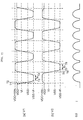
- Fig. 7 is a timing chart showing a charging operation of the charging circuit.
- Vt in the figure denotes the threshold voltages of the P-channel FETs P1 and P2.
- the P-channel FET P2 turns ON. Thereafter, the terminal voltage V1 falls, and will be below the low-potential power supply line VSS at time T2, and when it further falls by an amount of the voltage drop Vf of the diode D1 (at time T3), then the diode D1 turns ON. At this moment, since the terminal voltage V2 exceeds the threshold voltage Vt, the P-channel FET P1 turns OFF.
- the charging current i flows through the path: "the input terminal AG2 ⁇ the P-channel FET P2 ⁇ the high-potential power supply line VDD ⁇ the large-capacity capacitor 20 ⁇ the low-potential power supply line VSS ⁇ the diode D1", and the electric charge charges the large-capacity capacitor 20.
- the terminal voltage V2 falls when the terminal voltage V1 rises, and the terminal voltage V2 is below the threshold voltage Vt at time T5. Then, the P-channel FET P1 turns ON. Thereafter, the terminal voltage V2 falls, and is below the low-potential power supply line VSS at time T6, and further when it falls by an amount of the voltage drop Vf of the diode D2 (at time T7), the diode D2 turns ON. At this moment, since the terminal voltage V1 exceeds the threshold voltage Vt, the P-channel FET P2 turns OFF.
- the charging current flows through the path: "the input terminal AG1 ⁇ the P-channel FET P1 ⁇ the high-potential power supply line VDD ⁇ the large-capacity capacitor 20 ⁇ the low-potential power supply line VSS ⁇ the diode D2", and the electric charge charges the large-capacity capacitor 20.
- the generator voltage is full-wave rectified, and thus the charging current shown in Fig. 4(c) is obtained.
- the P-channel FET P1 turns ON when the terminal voltage V2 falls, and becomes lower than the threshold voltage Vt, and further when the terminal voltage V2 fulfills the condition of the above described equation 2, the limiter current ILIM flows through the path indicated by an arrow X1 in the figure.
- the limiter current ILIM flows through the path indicated by an arrow X2 in the figure.
- the input terminals AG1 and AG2 are shunted, and no charging current flows into the large-capacity capacitor 20 even when the terminal voltages V1 and V2 exceed the charging voltage Va, thereby making it possible to avoid overcharging of the large-capacity capacitor 20.
- the limiter current ILIM flows into the AC generator AG, an electromagnetic brake is applied to the rotor 14, and thus the charging circuit 101 has a self-control characteristic.
- the source and body of the limiter transistor LIMTr are connected to the high-potential power supply line VDD, there is no possibility that the body potential exceeds the source potential, and thus no limiter current ILIM flows during normal operation due to the backgate effect. As a result, the charging efficiency can be further enhanced.
- Fig. 8 is a circuit diagram of the charging circuit that is used in a wristwatch according to the third embodiment of the present invention.
- the points in the charging circuit 100'' of the present third embodiment that differ from the charging circuit 100 of the first embodiment are that, instead of the limiter transistor LIMTr which functions as the shunt unit 40, there are provided a limiter transistor LIMTr1 that is an enhancement-type N-channel FET, which is connected, in parallel with an N-channel FET N1, between the input terminal AG1 and the low-potential power supply line VSS, a gate terminal thereof being connected to an output terminal of the comparator COM; and a limiter transistor LIMTr2 that is an enhancement-type N-channel FET, which is connected, in parallel with an N-channel FET N2, between the input terminal AG2 and the low-potential power supply line VSS, a gate terminal thereof being connected to an output terminal of the comparator COM.
- a limiter transistor LIMTr1 that is an enhancement-type N-channel FET, which is connected, in parallel with an N-channel FET N1, between the input terminal AG1 and the low-potential power supply line VSS, a gate
- the limiter transistor LIMTr1 and the limiter transistor LIMTr2 have the same electrical characteristics, and in the present example, since they are configured with an N-channel, they turn OFF (open) when the control signal CS is at a low level, and they turn ON (connected) when the control signal CS is at a high level. Accordingly, when the charging voltage Va exceeds the predetermined voltage, the input terminals AG1 and AG2 are connected, and thus the limiter current ILIM flows, thereby no charging current i flows into the large-capacity capacitor 20.
- overvoltage detection is a detection operation which may be performed by sampling even when the detection is not being constantly performed.
- the comparator COM and the resistors R1 and R2 are configured such that the power supplies thereto are stopped with a transistor switch, and the power is supplied to the comparator COM and the resistors R1 and R2 by turning the transistor switch ON for a period of a few seconds, and the overvoltage detection is performed, thereby reducing the current consumed according to the detection operation.
- a latch circuit may preferably be provided at an output of the comparator in order to maintain an output signal of the comparator during the sampling period.
- this charging circuit 100'' has a self-control characteristic such that the limiter current ILIM is reduced by forming a path for shunting.
- the circuit scale can be made small, and also the current consumed can be reduced.
- the shunt unit 40 is configured with the limiter transistor LIMTr1 and the limiter transistor LIMTr2 that are both N-channel FETs, and are controlled so that the limiter transistor LIMTr1 and the limiter transistor LIMTr2 are simultaneously turned ON when the charging voltage Va' that is divided from the charging voltage Va exceeds the reference voltage Vref, the charging voltage Va will never exceed the breakdown voltage of the large-capacity capacitor 20, thereby enabling the prevention of overcharging of the large-capacity capacitor 20.
- the shunt unit 40 is arranged to flow the generator current through a path that will not go through the diodes D1 and D2, but not by disconnecting the rectification unit 10 and the large-capacity capacitor 20, a transistor with a low breakdown voltage can be used for the one that is utilized in the shunt unit 40, thereby it is easily made as an IC. Further, when shunting the input terminals AG1 and AG2, a short brake is applied, so that the amplitudes of the terminal voltages V1 and V2 cap be lowered automatically.
- the source and body of the limiter transistor LIMTr are connected to the high-potential power supply line VDD, there is no possibility that the body potential exceeds the source potential, and thus no limiter current ILIM flows during normal operation due the backgate effect. As a result, the charging efficiency can be further enhanced.
- Fig. 9 is a circuit diagram of the charging circuit that is used in a wristwatch according to the fourth embodiment of the present invention.
- the main part of the charging circuit 100''' is comprised of a rectification unit 10 for rectifying a generator voltage of an AC generator AG, a large-capacity capacitor 20 for storing a charging current, a comparison unit 30 for detecting a charging voltage Va of the large-capacity capacitor 20 and for comparing the charging voltage Va with a reference voltage Vref, and a shunt unit 40 for shunting the high-potential power supply line VDD and the low-potential power supply line VSS based on the detection result of the comparison unit 30, and a reversed-current-prevention diode DRP for preventing a reversed current.
- d shown in the figure denotes a parasitic diode.
- the shunt unit 40 is comprised of a limiter transistor LIMTr.
- the limiter transistor LIMTr an enhancement-type P-channel transistor is used, and it is connected to the power supply lines VDD and VSS.
- the limiter current ILIM flows by shunting the high-potential power supply line VDD and the low-potential power supply line VSS, no charging current i flows into the large-capacity capacitor 20.
- the reversed-current-prevention diode DRP prevents the limiter current ILIM from flowing into the large-capacity capacitor 20 as the charging current i.
- Vt denotes the threshold voltages of the N-channel FET N1 and N2.
- the N-channel FET N2 turns ON. Thereafter, the terminal voltage rises, and exceeds the potential of the high-potential power supply line VDD, and further, when it rises by an amount of the voltage drop Vf of the diode D1 (at time T3), the diode D1 turns ON. At this moment, since the terminal voltage V2 is below the threshold voltage Vt, the N-channel FET N1 is OFF.
- the charging current i flows through the path: "the input terminal AG1 ⁇ the diode D1 ⁇ the high-potential power supply line VDD ⁇ the large-capacity capacitor 20 ⁇ the reversed flow prevention diode DRP ⁇ the low-potential power supply line VSS ⁇ the N-channel FET N2", and the electric charge charges the large-capacity capacitor 20.
- the terminal voltage V2 rises when the terminal voltage V1 falls, and the terminal voltage V2 exceeds the threshold voltage Vt at time T5. Then, the N-channel FET N1 turns ON. Thereafter, the terminal voltage V2 rises, and exceeds the high-potential power supply line VDD at time T6, and further when it rises by an amount of the voltage drop Vf of the diode D2 (at time T7), the diode D2 turns ON. At this moment, since the terminal voltage V1 is below the threshold voltage Vt, the N-channel FET N2 is OFF.
- the charging current i flows through the path: "the input terminal AG2 ⁇ the diode D2 ⁇ the high-potential power supply line VDD ⁇ the large-capacity capacitor 20 ⁇ the low-potential power supply line VSS ⁇ the reversed-current-prevention diode DRP ⁇ the N-channel FET N1", and the electric charge charges the large-capacity capacitor 20.
- the generator voltage is full-wave rectified, and thus the charging current i shown in Fig. 4(c) is obtained.
- step S2 since the limiter transistor LIMTr switches from OFF to ON (step S2), the high-potential power supply line VDD and the low-potential power supply line VSS are shunted, and, for example, when the terminal voltage AG1 (V1) rises and the terminal voltage AG2 (V2) falls, the limiter current ILIM flows through the path indicated by an arrow X in the figure.
- this charging circuit 100 has a self-control characteristic such that the limiter current ILIM is reduced by forming a path for shunting.
- the circuit scale can be made small, and also the current consumed can be reduced.
- the shunt unit 40 is configured with a field effect transistor, and is arranged to be controlled such that the limiter transistor turns ON when the voltage Va', of which the charging voltage Va is divided, exceeds the reference voltage Vref, the charging voltage Va will never exceed the breakdown voltage of the large-capacity capacitor 20, thereby enabling the prevention of overcharging of the large-capacity capacitor 20.
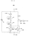
- Fig. 18 is a circuit diagram of a voltage-detection determination unit that is another embodiment of the voltage-detection determination unit of the first embodiment.
- the same symbols and references are attached to the parts or elements that are the same as the first embodiment in Fig. 1.
- a voltage-detection determination unit 30A is comprised of a constant current source CCNST in which one end thereof is connected to a power supply VDD, a transistor Q1 in which a drain D and a gate G thereof are commonly connected to the other end of the constant current source CCNST, a transistor Q2 in which a drain D and a gate G thereof are commonly connected to a source S of the transistor Q1, a pull-down resistor RPD in which one end thereof is connected to the power supply VDD, a first inverter INV1 in which an input terminal thereof is connected to the other end of the pull-down resistor RPD, a second inverter INV2 in which an input terminal thereof is connected to an output terminal of the first inverter INV1 and for outputting a control signal CS, and a current mirror circuit CMC that is connected between a source S of the transistor Q2 and the other end of the pull-down resistor RPD as well as to a power supply VSS.
- the current mirror circuit CMC is comprised of a transistor QD in which a drain D and a gate G thereof are commonly connected to a source S of the transistor Q2, and a transistor QC in which a drain D thereof is connected to the other end of the pull-down resistor RPD, a gate G thereof is connected to the gate G of the transistor QD, and a source S thereof is connected to the power supply VSS.
- the limiter transistor 40 maintains OFF.
- the current that flows through the transistor QC is set to be larger than a current that may flow through the pull-down resistor RPD, and, as a result, the voltage V1 becomes a voltage which is equivalent to the "L" level.
- the limiter transistor 40 turns ON, and thus the limiter current flows.
- the voltage-detection determination unit 30A' in the fifth embodiment does not substantially consumes current when the power source voltage is low, thus it is suitable for a circuit which prevents an overvoltage in portable electronic equipment that is driven by a battery and the like.
- the present invention as described above, it is arranged that when the charging voltage exceeds a predetermined voltage, a generator current that is output from one of the input terminals is supplied to the other one of the input terminals through a path that does not pass through the first and second diodes, thus overcharging of the charging element can be prevented. Further, since no comparator is used for controlling the switching means, the circuit scale can be made small, and a low consumption power can be further reduced.
- both input terminals are shunted by this gate, and thus overcharging of the charging element can be prevented with a simple configuration.
- the manufacturing cost can be reduced, and further, it facilitates the integration of the charging circuit into electronic equipment such as a wristwatch, in which the requirement of saving space is severe.
Landscapes
- Engineering & Computer Science (AREA)
- Power Engineering (AREA)
- Charge And Discharge Circuits For Batteries Or The Like (AREA)
- Electromechanical Clocks (AREA)
- Rectifiers (AREA)
- Secondary Cells (AREA)
- Control Of Charge By Means Of Generators (AREA)
- Direct Current Feeding And Distribution (AREA)
- Electric Clocks (AREA)
Applications Claiming Priority (3)
| Application Number | Priority Date | Filing Date | Title |
|---|---|---|---|
| JP7030198 | 1998-03-19 | ||
| JP7030198 | 1998-03-19 | ||
| PCT/JP1999/001383 WO1999048184A1 (fr) | 1998-03-19 | 1999-03-19 | Procede de prevention des surcharges, circuit chargeur, dispositif electronique et compteur de temps |
Publications (3)
| Publication Number | Publication Date |
|---|---|
| EP0998004A1 true EP0998004A1 (fr) | 2000-05-03 |
| EP0998004A4 EP0998004A4 (fr) | 2004-03-24 |
| EP0998004B1 EP0998004B1 (fr) | 2006-10-11 |
Family
ID=13427511
Family Applications (1)
| Application Number | Title | Priority Date | Filing Date |
|---|---|---|---|
| EP99909251A Expired - Lifetime EP0998004B1 (fr) | 1998-03-19 | 1999-03-19 | Procede de prevention des surcharges, circuit chargeur, dispositif electronique et compteur de temps |
Country Status (6)
| Country | Link |
|---|---|
| US (1) | US6429624B2 (fr) |
| EP (1) | EP0998004B1 (fr) |
| JP (1) | JP3472878B2 (fr) |
| CN (1) | CN100525003C (fr) |
| DE (1) | DE69933522T2 (fr) |
| WO (1) | WO1999048184A1 (fr) |
Families Citing this family (12)
| Publication number | Priority date | Publication date | Assignee | Title |
|---|---|---|---|---|
| KR101060141B1 (ko) * | 2004-08-23 | 2011-08-30 | 세미컨덕터 콤포넨츠 인더스트리즈 엘엘씨 | 전지 보호 방법 및 그의 구조 |
| KR100659272B1 (ko) * | 2005-12-15 | 2006-12-20 | 삼성전자주식회사 | 과전압 제어가 가능한 무선인증용 태그 및 그의 과전압제어 방법 |
| US8654549B2 (en) * | 2011-06-25 | 2014-02-18 | Jlj, Inc. | Battery polarity control system |
| WO2013182867A1 (fr) * | 2012-06-05 | 2013-12-12 | Freescale Semiconductor, Inc. | Procédé et appareil pour le chargement d'un dispositif de stockage de charge d'amorçage |
| CN103036293A (zh) * | 2012-12-12 | 2013-04-10 | 辽宁省电力有限公司锦州供电公司 | Ftu用电源 |
| US10176605B2 (en) * | 2014-03-26 | 2019-01-08 | Brigham Young University | Dynamic display of heirarchal data |
| US10389804B2 (en) * | 2015-11-11 | 2019-08-20 | Adobe Inc. | Integration of content creation and sharing |
| TWI639421B (zh) * | 2016-11-10 | 2018-11-01 | 睿傳數據股份有限公司 | 智慧床頭卡及其控制管理系統 |
| WO2019111872A1 (fr) | 2017-12-04 | 2019-06-13 | 株式会社Gsユアサ | Dispositif de commande de charge, dispositif de stockage d'électricité, et procédé de charge |
| US11383975B2 (en) | 2020-05-25 | 2022-07-12 | Silican Inc. | Composite for generating hydrogen |
| DE102020130728A1 (de) * | 2020-11-20 | 2022-05-25 | Osram Gmbh | Ansteuerbeschaltung für den steuereingang eines leistungstransistors eines getakteten wandlers und anwendung der ansteuerbeschaltung |
| CN115037168B (zh) * | 2021-02-25 | 2026-03-10 | 精工爱普生株式会社 | 整流电路以及受电控制装置 |
Family Cites Families (9)
| Publication number | Priority date | Publication date | Assignee | Title |
|---|---|---|---|---|
| US4365241A (en) * | 1978-09-12 | 1982-12-21 | Mitsubishi Denki Kabushiki Kaisha | Device for indicating the charging state of a battery |
| JPS58162875A (ja) * | 1982-03-23 | 1983-09-27 | Mitsubishi Electric Corp | 充電表示兼警報装置 |
| US4698740A (en) * | 1986-02-14 | 1987-10-06 | Westinghouse Electric Corp. | Current fed regulated voltage supply |
| JPS63137541U (fr) * | 1987-02-26 | 1988-09-09 | ||
| JP2652057B2 (ja) * | 1988-01-25 | 1997-09-10 | セイコーエプソン株式会社 | 発電装置 |
| FR2648966B1 (fr) * | 1989-06-27 | 1991-10-04 | Alsthom Gec | Circuit redresseur de signaux electriques alternatifs |
| EP0564149B1 (fr) * | 1992-04-03 | 1997-09-24 | JEOL Ltd. | Alimentation d'énergie avec condensateur de stockage |
| NO301917B1 (no) * | 1995-02-01 | 1997-12-22 | Fieldbus International As | Vekselström/likespennings-omformer |
| JP3204160B2 (ja) * | 1997-05-12 | 2001-09-04 | インターナショナル・ビジネス・マシーンズ・コーポレーション | バッテリパック及び電気・電子機器 |
-
1999
- 1999-03-19 WO PCT/JP1999/001383 patent/WO1999048184A1/fr not_active Ceased
- 1999-03-19 EP EP99909251A patent/EP0998004B1/fr not_active Expired - Lifetime
- 1999-03-19 CN CNB99800782XA patent/CN100525003C/zh not_active Expired - Fee Related
- 1999-03-19 JP JP54237999A patent/JP3472878B2/ja not_active Expired - Fee Related
- 1999-03-19 DE DE69933522T patent/DE69933522T2/de not_active Expired - Lifetime
- 1999-03-19 US US09/423,785 patent/US6429624B2/en not_active Expired - Lifetime
Also Published As
| Publication number | Publication date |
|---|---|
| DE69933522T2 (de) | 2007-06-06 |
| WO1999048184A1 (fr) | 1999-09-23 |
| EP0998004A4 (fr) | 2004-03-24 |
| EP0998004B1 (fr) | 2006-10-11 |
| HK1026524A1 (en) | 2000-12-15 |
| DE69933522D1 (de) | 2006-11-23 |
| CN1272236A (zh) | 2000-11-01 |
| JP3472878B2 (ja) | 2003-12-02 |
| US20020011821A1 (en) | 2002-01-31 |
| US6429624B2 (en) | 2002-08-06 |
| CN100525003C (zh) | 2009-08-05 |
Similar Documents
| Publication | Publication Date | Title |
|---|---|---|
| US8160654B2 (en) | Power reception control device, power reception device, and electronic instrument | |
| JP3472879B2 (ja) | 過充電防止方法、充電回路、電子機器および時計 | |
| US6324084B1 (en) | Power supply device, power supply method, portable electronics apparatus, and electronic timepiece | |
| US6421261B1 (en) | Power supply apparatus with unidirectional units | |
| EP0998004B1 (fr) | Procede de prevention des surcharges, circuit chargeur, dispositif electronique et compteur de temps | |
| JPWO2000033454A1 (ja) | 電力供給装置、電力供給方法、携帯型電子機器および電子時計 | |
| US6693851B1 (en) | Electronic device and control method for electronic device | |
| JPWO1999060684A1 (ja) | 過充電防止方法、充電回路、電子機器および時計 | |
| US11146081B2 (en) | Circuit device, control device, power receiving device, and electronic device | |
| US6476580B1 (en) | Electronic apparatus and control method for electronic apparatus | |
| US6327164B1 (en) | Chopper circuit, chopper circuit control method, chopper-type charging circuit, electronic device, and timekeeping apparatus | |
| US6421263B1 (en) | AC voltage detection circuit and method, charging circuit and method, chopper circuit and chopping method, chopper charging circuit and method, electronic apparatus, and timepiece | |
| JPWO1999048184A1 (ja) | 過充電防止方法、充電回路、電子機器および時計 | |
| JP3663964B2 (ja) | 過充電防止方法、充電回路、電子機器および時計 | |
| JP5176810B2 (ja) | 整流制御装置、全波整流回路、受電装置、無接点電力伝送システムおよび電子機器 | |
| JP7052326B2 (ja) | 電源装置及び通信装置 | |
| EP1098234B1 (fr) | Dispositif électronique et procédé de contrôle pour ce dispositif | |
| US6304474B1 (en) | Chopper circuit, chopper circuit control method, chopper-type charging circuit, electronic device, and timekeeping apparatus | |
| US6353522B1 (en) | Switching state detecting device for switch, and electronic apparatus | |
| HK1026524B (en) | Method of overcharge prevention, charger circuit, electronic device, and timepiece | |
| JPH11187667A (ja) | 電源装置、発電装置および電子機器 | |
| JP2003235167A (ja) | 過充電防止方法、充電回路、電子機器および時計 | |
| JP2004032980A (ja) | 過充電防止方法、充電回路、電子機器および時計 | |
| HK1034817A (en) | Chopper circuit and chopper circuit control method | |
| HK1029670B (en) | Overcharge protection, charger, electronic device and timepiece |
Legal Events
| Date | Code | Title | Description |
|---|---|---|---|
| PUAI | Public reference made under article 153(3) epc to a published international application that has entered the european phase |
Free format text: ORIGINAL CODE: 0009012 |
|
| AK | Designated contracting states |
Kind code of ref document: A1 Designated state(s): CH DE FR GB LI |
|
| 17P | Request for examination filed |
Effective date: 20000315 |
|
| A4 | Supplementary search report drawn up and despatched |
Effective date: 20040209 |
|
| RIC1 | Information provided on ipc code assigned before grant |
Ipc: 7H 02M 7/217 B Ipc: 7H 02J 1/00 A |
|
| 17Q | First examination report despatched |
Effective date: 20040629 |
|
| GRAP | Despatch of communication of intention to grant a patent |
Free format text: ORIGINAL CODE: EPIDOSNIGR1 |
|
| GRAS | Grant fee paid |
Free format text: ORIGINAL CODE: EPIDOSNIGR3 |
|
| GRAA | (expected) grant |
Free format text: ORIGINAL CODE: 0009210 |
|
| AK | Designated contracting states |
Kind code of ref document: B1 Designated state(s): CH DE FR GB LI |
|
| REG | Reference to a national code |
Ref country code: GB Ref legal event code: FG4D |
|
| REG | Reference to a national code |
Ref country code: CH Ref legal event code: EP |
|
| REF | Corresponds to: |
Ref document number: 69933522 Country of ref document: DE Date of ref document: 20061123 Kind code of ref document: P |
|
| ET | Fr: translation filed | ||
| REG | Reference to a national code |
Ref country code: HK Ref legal event code: GR Ref document number: 1026524 Country of ref document: HK |
|
| PLBE | No opposition filed within time limit |
Free format text: ORIGINAL CODE: 0009261 |
|
| STAA | Information on the status of an ep patent application or granted ep patent |
Free format text: STATUS: NO OPPOSITION FILED WITHIN TIME LIMIT |
|
| 26N | No opposition filed |
Effective date: 20070712 |
|
| REG | Reference to a national code |
Ref country code: FR Ref legal event code: PLFP Year of fee payment: 17 |
|
| PGFP | Annual fee paid to national office [announced via postgrant information from national office to epo] |
Ref country code: DE Payment date: 20150310 Year of fee payment: 17 Ref country code: CH Payment date: 20150313 Year of fee payment: 17 |
|
| PGFP | Annual fee paid to national office [announced via postgrant information from national office to epo] |
Ref country code: GB Payment date: 20150318 Year of fee payment: 17 Ref country code: FR Payment date: 20150309 Year of fee payment: 17 |
|
| REG | Reference to a national code |
Ref country code: DE Ref legal event code: R119 Ref document number: 69933522 Country of ref document: DE |
|
| REG | Reference to a national code |
Ref country code: CH Ref legal event code: PL |
|
| GBPC | Gb: european patent ceased through non-payment of renewal fee |
Effective date: 20160319 |
|
| REG | Reference to a national code |
Ref country code: FR Ref legal event code: ST Effective date: 20161130 |
|
| PG25 | Lapsed in a contracting state [announced via postgrant information from national office to epo] |
Ref country code: DE Free format text: LAPSE BECAUSE OF NON-PAYMENT OF DUE FEES Effective date: 20161001 Ref country code: FR Free format text: LAPSE BECAUSE OF NON-PAYMENT OF DUE FEES Effective date: 20160331 Ref country code: LI Free format text: LAPSE BECAUSE OF NON-PAYMENT OF DUE FEES Effective date: 20160331 Ref country code: GB Free format text: LAPSE BECAUSE OF NON-PAYMENT OF DUE FEES Effective date: 20160319 Ref country code: CH Free format text: LAPSE BECAUSE OF NON-PAYMENT OF DUE FEES Effective date: 20160331 |