EP0998047A2 - Dispositif à nombre réduit d'états et méthode de décodage de données - Google Patents
Dispositif à nombre réduit d'états et méthode de décodage de données Download PDFInfo
- Publication number
- EP0998047A2 EP0998047A2 EP99308371A EP99308371A EP0998047A2 EP 0998047 A2 EP0998047 A2 EP 0998047A2 EP 99308371 A EP99308371 A EP 99308371A EP 99308371 A EP99308371 A EP 99308371A EP 0998047 A2 EP0998047 A2 EP 0998047A2
- Authority
- EP
- European Patent Office
- Prior art keywords
- winning
- states
- acps
- memory array
- pss
- Prior art date
- Legal status (The legal status is an assumption and is not a legal conclusion. Google has not performed a legal analysis and makes no representation as to the accuracy of the status listed.)
- Ceased
Links
- 238000000034 method Methods 0.000 title claims abstract description 56
- 230000015654 memory Effects 0.000 claims description 139
- 238000003491 array Methods 0.000 claims description 8
- 238000004590 computer program Methods 0.000 claims description 6
- 238000010586 diagram Methods 0.000 description 10
- 101100135116 Oryza sativa subsp. japonica RR12 gene Proteins 0.000 description 5
- 230000005540 biological transmission Effects 0.000 description 5
- 239000013256 coordination polymer Substances 0.000 description 4
- 238000010845 search algorithm Methods 0.000 description 3
- 238000004891 communication Methods 0.000 description 2
- 101150116266 RR24 gene Proteins 0.000 description 1
Images


Classifications
-
- H—ELECTRICITY
- H03—ELECTRONIC CIRCUITRY
- H03M—CODING; DECODING; CODE CONVERSION IN GENERAL
- H03M13/00—Coding, decoding or code conversion, for error detection or error correction; Coding theory basic assumptions; Coding bounds; Error probability evaluation methods; Channel models; Simulation or testing of codes
- H03M13/03—Error detection or forward error correction by redundancy in data representation, i.e. code words containing more digits than the source words
- H03M13/23—Error detection or forward error correction by redundancy in data representation, i.e. code words containing more digits than the source words using convolutional codes, e.g. unit memory codes
-
- H—ELECTRICITY
- H03—ELECTRONIC CIRCUITRY
- H03M—CODING; DECODING; CODE CONVERSION IN GENERAL
- H03M13/00—Coding, decoding or code conversion, for error detection or error correction; Coding theory basic assumptions; Coding bounds; Error probability evaluation methods; Channel models; Simulation or testing of codes
- H03M13/37—Decoding methods or techniques, not specific to the particular type of coding provided for in groups H03M13/03 - H03M13/35
- H03M13/39—Sequence estimation, i.e. using statistical methods for the reconstruction of the original codes
Definitions
- the present invention relates to a device and method for decoding data and, more particularly, to a reduced-state device and method for decoding data by generating accumulated conditional probabilities (ACPs) for certain states out of all possible states of an encoder.
- ACPs accumulated conditional probabilities
- a conventional convolutional encoder encodes information bits using a shift register and a plurality of adders.
- Fig. 1 shows a schematic diagram of a conventional 1 ⁇ 2 rate convolutional encoder.
- the conventional convolutional encoder 100 includes a shift register 11 composed of a plurality of memory units M0-M7 connected in series to each other, and first and second adders 10 and 12 coupled to the shift register 11 for generating first and second coefficients C0 and C1.
- Each of the memory units M0-M7 is a one-bit memory for storing a bit input thereto while shifting the bit already stored therein to a next one-bit memory.
- the shift register 11 Since there are 8 one-bit memory units M0-M1 in the shift register 11, the shift register 11 has 256 possible states (from state 0 to state 255).
- state indicates the content of the shift register 11 at a given time. It is known that the state of the shift register 11 is an even state if the arriving information bit (i.e., the bit ready to be input to the first memory unit M0) of the previous state of the shift register 11 is zero, or an odd state if the arriving information bit of the previous state of the shift register 11 is one.
- An operation of the conventional convolutional encoder 100 of Fig. 1 is as follows.
- Information bits to be encoded are input to the first memory unit M0 one bit at a time.
- a block of information bits (e.g., 196 bits) are typically processed at one time.
- Each new information bit input to the encoder 100 is pushed into the first memory unit M0 of the shift register 11 as the previous content of the first memory unit M0 is shifted to the second memory unit M1, the previous content of the second memory unit M1 to the third memory unit M2, the previous content of the third memory unit M2 to the fourth memory unit M3, and so forth.
- a controller (not shown) generates a clock signal to shift the bits of the memory units M0-M7 at a predetermined time interval.
- the first adder 10 adds the arriving information bit of the shift register 11 with bits stored in the memory units M0, M1, M2, M4, M6, and M7 to generate the first coefficient C0.
- the second adder 12 adds the arriving information bit with bits stored in the memory units M1, M2, M3 and M7 to generate the second coefficient C1.
- a pair of coefficients C0 and C1 are output from the encoder 100 as encoded data.
- the encoder 100 has the 1 ⁇ 2 process rate.
- the conventional 1 ⁇ 2 rate convolutional encoder 100 has been described above, encoders having other process rates, e.g., 1/3, 2/3, and others, are also known in the art.
- the first and second coefficients C0 and C1 (encoded data) generated by the encoder 100 pass through communication channels to other encoders/decoders. During this process, however, the encoded data suffer from bit corruption and become less reliable. For example, as the encoded data pass through communication channels, certain zero ("0") bits may change to one ("1") bits and vice versa, such that corrupted coefficients CC0 and CC1 are transmitted as encoded data, and are decoded by a conventional convolutional decoder.
- a conventional convolutional decoder assumes all possible states of the shift register 11 of the encoder 100, and attempts to determine what the original, uncorrupted coefficients C01 and C1 are. If the original coefficients C0 and C1 output from the encoder 100 can be determined, then accurate input data (i.e., arriving information bits of the encoder 100) can be recovered as decoded data.
- Fig. 2 shows a block diagram of such a conventional convolutional decoder 200 for decoding encoded data, such as, corrupted coefficients CC0 and CC1.
- the decoder 200 includes a state counter 20, a previous state locator 22, first and second encoders 24A and 24B, a modulo 2 unit 26, first and second quantizers 28A and 28B, first and second adders 30A and 30B, a maximum selector 32, a memory unit 34, and a decoding unit 36, connected as shown.
- the state counter 20 counts from state 0 to state 255 for each pair of the corrupted coefficients CC0 and CC1 to cover all 256 possible states of the shift register 11 in the conventional encoder 100.
- the state counting by the state counter 20 is performed based on a clock signal generated from the memory unit 34.
- the previous state locator 22 determines two possible previous states (i.e., two possible contents of the memory units M0-M7 of the shift register 11 shown in Fig. 1) according to a known process.
- One of the two possible previous states is output to the first encoder 24A, and the other possible previous state is output to the second encoder 24B.
- the modulo 2 unit 26 receives the state count value from the state counter 20, and generates 0 or 1 based on each state count value.
- the 0 and 1 output from the modulo 2 unit 26 represent possible information bits (0 and 1) to be recovered by the decoder 200.
- Each of the first and second encoders 24A and 24B receives the bit from the modulo 2 unit 26 and one of the two possible previous states determined by the previous state locator 22 to generate theoretical coefficients TC0 and TC 1. For each input to the first and second encoders 24A and 24B, the first encoder 24A generates a pair of first theoretical coefficients TC0 and TC1, and the second encoder 24B generates a pair of second theoretical coefficients TC0 and TC1. This process is repeated for each of the 256 possible states, so that 256 pairs of theoretical coefficients TC0 and TC1 are sequentially output from each of the first and second encoders 24A and 24B.
- Each of the first and second quantizers 28A and 28B receives a pair of the theoretical coefficients TC0 and TC1 for each state count value, and encoded data bits (pairs of corrupted coefficients CC0 and CC1) input to the decoder 200.
- Each of the first and second quantizers 28A and 28B determines, assuming that uncorrupted coefficients C0 and C1 are input to the decoder 200, the conditional probability of each pair of the corrupted coefficients CC0 and CC1 based on the sequentially received pairs of theoretical coefficients TC0 and TC1, and then quantizes the conditional probability into a certain number of levels, e.g., 32 or 64 levels.
- the quantized values output from each of the first and second quantizers 28A and 28B indicate how well each pair of inputted corrupted coefficients CC0 and CC1 match the 256 pairs of theoretical coefficients TC0 and TC1. Accordingly, the conventional convolutional decoder 100 carries out a full search algorithm by determining conditional probabilities for the entire 256 possible states of the encoder 100.
- each of the first and second adders 30A and 30B adds the current quantized value with the corresponding accumulated quantized value (i.e., ACP) stored in the memory unit 34 to generate updated ACPs.
- the maximum selector 32 receives two ACPs from the adders 30A and 30B at a given time, compares the two ACPs to each other, and selects the greater one of the two ACPs.
- the selected ACP is referred to hereinafter as the winning ACP, and the previous state which results in the winning ACP is referred to hereinafter as the winning previous state (PS).
- the winning ACP and PS are output to the memory unit 34 unit, where the winning ACP replaces the ACP currently stored in a data slot of the memory unit 34 corresponding to the current state count value.
- the memory unit 34 must store 0 to 255 possible ACPs and their corresponding PSs for each of the 196 information bits, and must update all 256 ACPs using the outputs of the maximum selector 32. To carry out this process and the process by the decoding unit 36, the memory unit 34 requires a 256 X 196 memory array for storing winning PSs in addition to other memory arrays for storing winning ACPs.
- Fig. 2A shows an example of a 256 X 196 memory array 34a of the memory unit 34 for storing winning PSs.
- the memory array 34a of the memory unit 34 is composed of 256 rows (R0 - R255) and 196 columns (C0-C195). Each row number represents the current state value and each column number represents a bit in the 196 information bits.
- the memory unit 34 stores in its array 34a the PSs corresponding to the entire 256 possible states. For example, if the current state is zero (i.e., R0), the 196 th information bit is being decoded by the decoder 200, and the winning PS for this particular current state has been determined to be three (3) by the maximum selector 200, then the wining PS of 3 is stored in a data slot (R0, C195) of the array 34a.
- the decoding unit 36 begins to recover the original information bits using the array 34a.
- the decoding unit 36 first retrieves the winning PS of 3 from the slot (R0, C195) of the array 34a. Since the winning PS equals 3, the decoding unit 36 goes to row R3 in the next column, C194, and retrieves the winning PS of 1 therefrom. Since the winning PS here equals 1, the decoding unit 36 goes to row R1 in the next column, C193, and retrieves the winning PS of 255 therefrom. Since the winning PS now equals 255, the decoding unit 36 goes to row R255 in the next column, C192, and retrieves the winning PS of 62 therefrom. This process is repeated until the last column C0 is searched.
- 196 integers are sequentially collected by the decoding unit 36. Depending on whether each of the 196 integers is an odd number or an even number, zero (0) or one (1) bit is output from the decoding unit 36 as decoded data representing the original 196 information bits.
- the present invention is directed to a reduced-state device and method for decoding data that uses less memory for storing winning previous states (PSs) associated with accumulated conditional probabilities (ACPs) because less ACPs are generated.
- the reduced-state device and method select only certain current states from all possible states of an encoder for each encoded data based on a control signal, and generate ACPs for the selected current states.
- a predetermined quantized value PQV
- the ACPs and the PQV are compared with a threshold value. If the ACP/PQV is greater than or equal to the threshold value, a PS associated with such ACP/PQV is stored in a first memory array.
- a second memory array stores the positional information of the first memory array in which the winning PS is stored. From each column of the first memory array, one of the values stored therein is selected based on the value selected from the previous column. These selected values are converted into 0 or 1 bit, and the converted data bits are output as decoded data. Accordingly, the present invention generates ACPs only for certain states out of all possible states and thus, requires less memory for storing PSs associated with the ACPs. Furthermore, the present invention provides a faster decoding process since a reduced number of states are searched to generate decoded data.
- the following detailed description relates to a decoder and its method for decoding data according to the present invention.
- states e.g., states most likely to occur
- the method of the present invention can be implemented using computers, computer programs, or the like.
- the decoder of the present invention decodes encoded data (pairs of corrupted coefficients CC0 and CC1) which have been output from a 8-bit shift register (having 256 possible states) of an encoder, e.g., the shift register 11 shown in Fig. 1.
- the present device and method can be implemented for decoding other encoded data generated using other types of encoders or a shift register of a different size.
- Fig. 3 shows a block diagram of a decoder 300 according to the present invention.
- the decoder 300 includes a state counter 40, a previous state locator 42, a state selector 46, a modulo 2 unit 48, a plurality of encoders 50A and 50B, a plurality of quantizers 52A and 52B, a plurality of adders 54A and 54B, a maximum selector 58, a first memory unit 60A, a second memory unit 60B, a comparator 62, a threshold estimator 64, and a decoding unit 68.
- the state counter 40 can be a shift register known in the art, and the previous state locator 42, the modulo 2 unit 48, the encoders 50A and 50B, the quantizers 52A and 52B, the adders 54A and 54B, and the maximum selector 58 are known elements as shown in Fig. 1.
- the state counter 40 counts from possible state 0 to possible state 255 based on a clock signal generated from the first memory unit 60A.
- the state counter 40 can be a shift register or other counting devices known in the art. Although the state counter 40 counts 256 possible states in this example, a different number of possible states can be counted depending on the size of the encoder, etc.
- the state counter 40 outputs each state count value to both the modulo 2 unit 48 and the previous state locator 42. For each state count value, the previous state locator 42 determines two possible previous states PS1 and PS2. If a current state is "N" and the total number of possible states is "M", then it is known in the art that the corresponding two possible previous states are "N/2" and "(N+M)/2".
- the previous state locator 42 determines that the two possible previous states corresponding to the current state (state 5) are "state 2" (2 ⁇ 5/2) and "state 130" (130 ⁇ (5+256)/2). As in this example, if the division results in a decimal number, the decimal number is rounded down.
- the previous state locator 42 then outputs the two possible previous states PS1 and PS2 (e.g., state 2 and state 130) to the state selector 46 through first and second input lines 70A and 70B, respectively.
- Fig. 4 shows a detailed block diagram of the state selector 46.
- the state selector 46 includes first and second transmitters 73A and 73B, and first and second memories 75A and 75B connected to the first and second transmitters 73A and 73B, respectively.
- the first and second transmitters 73A and 73B can be implemented with a collection of logic gates known in the art.
- the first and second memories 75A and 75B prestore therein one predetermined quantized value (PQV).
- the PQV can be any value which is different from (preferably lower than) any of ACPs (for 256 states) stored in the first memory unit 60A.
- the PQV is a negative number, such as -1, while all ACPs stored in the first memory unit 60A are non-negative numbers.
- other numbers may be used as the PQV according to the present invention.
- the state selector 46 receives, through the first and second input lines 70A and 70B, a pair of possible previous states PS1 and PS2 (e.g., state 2 and state 130) for each of the 256 states counted by the state counter 40.
- An enable signal ENA or a disable signal DIS from the first memory unit 60A is applied simultaneously to both the first and second transmitters 73A and 73B of the state selector 46 through a connection 71.
- the first transmitter 73A receives the enable signal ENA from the first memory unit 60A, the first transmitter 73A transmits the first possible previous state PS1 (e.g., state 2) to the first encoder 50A through a first transmission line 72A.
- the second transmitter 73B receives the enable signal ENA from the first memory unit 60A, the second transmitter 73B transmits the second possible previous state PS2 (e.g., state 130) to the second encoder 50B through a second transmission line 72B.
- the first and second transmitters 73A and 73B disable the first and second memories 75A and 75B, respectively, so that no data are output from the memories 75A and 75B.
- the first transmitter 73A receives the disable signal DIS from the first memory unit 60A, the first transmitter 73A disables the first transmission line 72A and simultaneously enables the first memory 75A in order to output the PQV prestored in the first memory 75A to the maximum selector 58 through a first connection line 74A.
- the second transmitter 73B disables the second transmission line 72B and simultaneously enables the second memory 75B to output the same PQV prestored in the second memory 75B to the maximum selector 58 through a second connection line 74B.
- pairs of previous possible states PS1 and PS2 corresponding to certain current states are transmitted from the state selector 46 to the first and second encoders 50A and 50B through the first and second transmission lines 72A and 72B, respectively.
- the non- selected pairs of previous possible states PS1 and PS2 are discarded by the state selector 46, and instead, the PQV prestored in the memories 75A and 75B is transmitted to the maximum selector 58 through the first and second connection lines 74A and 74B.
- the modulo 2 unit 48 receives the state count values from the state counter 40, and generates any odd or even number, e.g., 0 or 1, based on each state count value. For example, the modular 2 unit 48 generates 0 if an odd state count value is received, and generates 1 if an even state count value is received.
- the 0 and 1 output from the modulo 2 unit 48 represent possible information bits (0 and 1) to be recovered by the decoder 300. In this example, given that the current state count is 5 (state 5), the modular 2 unit 48 generates 1 to the encoders 50A and 50B.
- the first encoder 50A receives the bit (e.g., 1) from the modulo 2 unit 48 and the first possible previous state PS1 (e.g., state 2) from the state selector 46, and generates a first pair of theoretical coefficients TC0 and TC1 based on these inputs.
- the second encoder 50B receives the same bit (i.e., 1) from the modulo 2 unit 48 and the second previous state PS2 (e.g., state 130) from the state selector 46, and generates a second pair of theoretical coefficients TC0 and TC1 based on these inputs. This process is repeated for each pair of possible previous states selected by the state selector 46.
- the first quantizer 52A receives the theoretical coefficients TC0 and TC1 from the first encoder 50A, and encoded data bits (e.g., corrupted coefficients CC0 and CC1) externally input to the decoder 300 for decoding.
- the second quantizer 52B receives the theoretical coefficients TC0 and TC1 from the second encoder 50B and the corrupted coefficients CC0 and CC1.
- Each of the first and second quantizers 52A and 52B determines the conditional probability of each pair of the corrupted coefficients CC0 and CC1 based on the pairs of theoretical coefficients TC0 and TC1 generated from the corresponding encoder 50A or 50B, and then quantizes each conditional probability into a predetermined number of levels, e.g., 32 levels, 64 levels, etc., to generate quantized values. For example, if about 40 states among the entire 256 possible states are selected by the state selector 46 (which generates about 80 previous states corresponding to the 40 selected states), each quantizer 52A, 52B generates 80 quantized values per 40 selected states for each pair of corrupted coefficients CC0 and CC1. These quantized values indicate how well the pair of corrupted coefficients CC0 and CC1 matches each pair of the theoretical coefficients TC0 and TC1.
- each of the first and second adders 54A and 54B adds the current quantized value with a corresponding accumulated quantized value (i.e., ACP) stored in the first memory unit 60A.
- ACP accumulated quantized value
- the first memory unit 60A includes a first memory array 90 having a data area 92 referenced by an index IN1, and a second memory array 93 having data area 95 referenced by an index IN2.
- the index numbers of the indexes IN1 and IN2 represent the possible 256 (Index 0 - Index 255) states such that the index number corresponds to the current state count.
- a pair of ACP and previous states PS (ACP 0 , ACP 1 , ACP 2 ...ACP 255 ; PS 0 , PS 1 , PS 2 ,..., PS 255 ) corresponding to Index 0 - Index 255 are stored, where the PQV is stored in lieu of the ACP depending on the state selector 46.
- the second memory array 93 stores in its data area 95 the conditional probabilities (CP 0 , CP 1 , CP 2 ,..CP 255 ) for each current state according to the index number. These values are output to the adders 54A and 54B in case the ACP of the current state has been just updated.
- the memory unit 60A includes other circuits for outputting the enable and disable signals ENS and DIS to the state selector 46 based on the data stored in the array 90. If the PQV is stored in the data area 92 corresponding to the index number matching the current state count, then the disable signal DIS is output to the state selector 46. Otherwise, the memory unit 60A outputs the enable signal ENS to the state selector 46.
- the first and second adders 54A and 54B then outputs a pair of new ACPs to the maximum selector 58.
- the maximum selector 58 compares the two ACPs to each other, selects the greater of the two ACPs to generate the winning ACP, and replaces the ACP/PQV currently stored under index 5 (current state) in the first memory array 90 with the winning ACP. If the maximum selector 58 receives the PQVs prestored in the memories 75A and 75B of the state selector 46 for the current state count, the maximum selector 58 updates the ACP/PQV currently stored under index 5 with the PQV.
- the first memory array 90 is a 256 X 2 array
- the second memory array 93 is a 256 X 1 array.
- memory arrays having different sizes can be used for the first memory unit 60A.
- the first memory unit 60A Once the data corresponding to all 256 index numbers have been generated and processed by the first memory unit 60A, the first memory unit 60A generates a control signal to the state counter 40 for starting the counting process from 0 again for the next pair of corrupted coefficients CC0 and CC1. In this example, this is carried out for 196 times since a block of encoded data being processed at one time has 196 information bits.
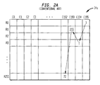
- Fig. 6 shows a detailed block diagram of the threshold estimator 64 of Fig. 3.
- the threshold estimator 64 includes a digitizer 80 for digitizing or quantizing the 256 ACPs/PQV corresponding to 256 states into certain preset values, a counter array 84 for generating accumulated values using the ACPs/PQV, and an array access logic (AAL) unit 86 for accessing an index number from the counter array 84 based on a threshold setting value (TSV) input thereto and outputting the index number as a threshold value h.
- the AAL unit 86 can be implemented using a collection of logic gates known in the art.
- the digitizer 80 of the threshold estimator 64 receives 256 sets of data from the data area 92 of the first memory unit 60A, quantizes these data to a predetermined number of levels, and outputs the quantized values to the counter array 84.
- the counter array 84 includes a first counter array 110 and a second counter array 113 as shown in Figs. 7A and 7B.
- the first counter array 110 includes a data area 112 for storing data corresponding to the index numbers of an index IN3.
- the second counter array 113 includes a data area 115 for storing data corresponding to the index numbers of an index IN4.
- the index numbers of the indexes IN3 and IN4 correspond to a range of possible quantized values output from the digitizer 80.
- the index numbers in the indexes IN3 and IN4 range from 0 to 100, sequentially, as shown in, e.g., Fig. 7A.
- the first counter array 110 receives the 256 quantized values from the digitizer 80, and counts how many times each quantized value occurs in the 256 quantized values. For example, as shown in Fig. 7A, if there exists five quantized value of "0", two quantized value of "1", three quantized value of "2",..., six quantized value of "97", zero quantized value of "98", three quantized value of "99", and one quantized value of "100", the first counter array 110 stores in the data area 112, values "5, 2, 3, ..., 6, 0, 3, 1" corresponding to the index numbers, "0, 1, 2,..., 97, 98, 99, 100", respectively.
- the second counter array 113 accesses the data stored in the data area 112 from the last index number, i.e., Index 100, and accumulates the data in the data area 115.
- the second counter array 113 will have, in this example, the value of "256" stored in the data area 115 somewhere between Index 96 and Index 0 of the second counter array 113.
- the AAL unit 86 receives a TSV from a user or an external source. The user can control the size of the second memory unit 60B by controlling the value of the TSV input to the AAL unit 86.
- the AAL unit 86 searches the data area 115 of the second counter array 113 for a data which matches the TSV. If there is no exact match, the AAL unit 86 looks for a data which is closest to the TSV. Once the matching data is found, the AAL unit 86 outputs the index number which corresponds to the matching data, and outputs this index number as the threshold value h to the comparator 62.
- the comparator 62 sequentially receives the data (ACP or PQV, PS) stored in the data area 92 of the first memory unit 60A for all 256 index numbers. As such data are sequentially received, the comparator 62 compares the threshold value h with the ACP/PQV received. If the received ACP/PQV is greater than or equal to the threshold value h, then the PS corresponding to the ACP/PQV passes to the second memory unit 60B. Otherwise, the received data are discarded and the next data corresponding to the next index number is compared and similarly processed.
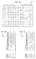
- Figs. 8A and 8B show examples of memory arrays of the second memory unit 60B according to the present invention.
- the second memory unit 60B includes a first memory array 120 and a second array 122.
- the first memory array 120 has a size of, e.g., 64 X 196
- the second memory array 122 has a size of, e.g., 256 X 2; however, memory arrays having various different sizes can be used depending on the TSV and/or other factors, e.g., data block size.
- Each column of the first memory array 120 represents one of the 196 information bits to be recovered.
- An example of a method of storing data in the second memory unit 60B according to the present invention is as follows.
- the first and second memory arrays 120 and 122 are initialized with a predetermined number, e.g., -1, before any data is stored therein. That is, any data slot marked with -1 indicates that it is empty.
- the winning PSs which correspond to the ACPs that passed the comparison test of the comparator 62, are sequentially output and stored in the first memory array 120 starting with the data slot (R0, C0) and down in the row direction (e.g., R1, R2, R3...R263 in column C0).
- Each winning PS is associated with a particular current state, and the array 120 is processed one column at a time where a column represents one information bit to be recovered. That is, once all the winning PSs for one column has been processed, then all the winning PSs for the next adjacent column is processed, and so on, until the last column (column C195) is processed.
- the index number (i.e., row number) of the second array 122 represents the winning PS.
- the decoding unit 68 accesses the winning PSs stored in the first array 120 from the last to the first column (C195 to C0) to recover the original information bits.
- An operation of generating decoded information bits using the data stored in the first array 120 is as follows.
- the decoding unit 68 searches the last column C195 of the array 120 for a value of zero since the last state of any data block is conventional known to be zero due to 8 tailing bits. Once a value of zero is found in row R0, then the value of zero is selected for the information bit position #195. Then the decoding unit 68 moves to the next left column and reads the value stored therein, i.e., to the slot (R1, C194). The decoding unit 68 moves to the next and reads each value it locates as long as the value of -1 is not detected. In this example, the value of -1 indicating that the slot is empty is located in the slot (R1, C194). Then, column R195 is searched from row R0 down to row R64 until another zero is found.
- the decoding unit 68 gathers 196 integers, and generates either 0 or 1 as the decoded data based on whether the integer is an odd or even number. For example, if the integer is an odd number, the decoding unit 68 outputs 1, and if the integer is an even number, the decoding unit 68 outputs 0, so that 196 information bits are output from the decoding unit 68 as decoded data. In this example, since the integers of 0, 128, 64, 32, 144...were found in the array 120, the decoded data of 0, 0, 0, 0, 0... are output from the decoding unit 68 as the decoded data.
- smaller memories can be used and a reduced-state search algorithm is performed, so as to decrease the cost of the device and method and to increase the operational speed of the device and method.
Landscapes
- Physics & Mathematics (AREA)
- Probability & Statistics with Applications (AREA)
- Engineering & Computer Science (AREA)
- Theoretical Computer Science (AREA)
- Compression, Expansion, Code Conversion, And Decoders (AREA)
- Complex Calculations (AREA)
- Error Detection And Correction (AREA)
Applications Claiming Priority (2)
| Application Number | Priority Date | Filing Date | Title |
|---|---|---|---|
| US181811 | 1998-10-29 | ||
| US09/181,811 US6408418B1 (en) | 1998-10-29 | 1998-10-29 | Reduced-state device and method for decoding data |
Publications (2)
| Publication Number | Publication Date |
|---|---|
| EP0998047A2 true EP0998047A2 (fr) | 2000-05-03 |
| EP0998047A3 EP0998047A3 (fr) | 2004-01-02 |
Family
ID=22665909
Family Applications (1)
| Application Number | Title | Priority Date | Filing Date |
|---|---|---|---|
| EP99308371A Ceased EP0998047A3 (fr) | 1998-10-29 | 1999-10-22 | Dispositif à nombre réduit d'états et méthode de décodage de données |
Country Status (8)
| Country | Link |
|---|---|
| US (1) | US6408418B1 (fr) |
| EP (1) | EP0998047A3 (fr) |
| JP (1) | JP3309371B2 (fr) |
| KR (1) | KR100606159B1 (fr) |
| CN (1) | CN1253419A (fr) |
| AU (1) | AU5597499A (fr) |
| BR (1) | BR9904738A (fr) |
| CA (1) | CA2281410A1 (fr) |
Families Citing this family (6)
| Publication number | Priority date | Publication date | Assignee | Title |
|---|---|---|---|---|
| US6690750B1 (en) * | 1999-12-23 | 2004-02-10 | Texas Instruments Incorporated | Flexible Viterbi decoder for wireless applications |
| JP3279289B2 (ja) | 1999-07-07 | 2002-04-30 | 神鋼電機株式会社 | 地下埋設設備の設置構造、及びその連結構造 |
| US20030188143A1 (en) * | 2002-03-28 | 2003-10-02 | Intel Corporation | 2N- way MAX/MIN instructions using N-stage 2- way MAX/MIN blocks |
| JP3651802B2 (ja) | 2002-09-12 | 2005-05-25 | 株式会社東芝 | 半導体装置の製造方法 |
| US9602243B2 (en) * | 2014-08-26 | 2017-03-21 | Electronics And Telecommunications Research Institute | Low density parity check encoder, and low density parity check encoding method using the same |
| EP4409748A1 (fr) * | 2021-09-27 | 2024-08-07 | Qualcomm Incorporated | Codage et/ou décodage efficace de données protégées contre une perte de paquets |
Family Cites Families (14)
| Publication number | Priority date | Publication date | Assignee | Title |
|---|---|---|---|---|
| US5263033A (en) * | 1990-06-22 | 1993-11-16 | At&T Bell Laboratories | Joint data and channel estimation using fast blind trellis search |
| DE4038251A1 (de) * | 1990-11-30 | 1992-06-04 | Philips Patentverwaltung | Entzerrer fuer ein digitales uebertragungssystem |
| US5229767A (en) * | 1991-09-05 | 1993-07-20 | Motorola, Inc. | Decoder for convolutionally encoded information |
| JP3120511B2 (ja) * | 1991-11-21 | 2000-12-25 | ソニー株式会社 | ビタビ復号装置 |
| US5390198A (en) * | 1993-05-26 | 1995-02-14 | The Boeing Company | Soft decision viterbi decoder for M-ary convolutional codes |
| FI94810C (fi) * | 1993-10-11 | 1995-10-25 | Nokia Mobile Phones Ltd | Menetelmä huonon GSM-puhekehyksen tunnistamiseksi |
| US5483236A (en) * | 1993-12-20 | 1996-01-09 | At&T Corp. | Method and apparatus for a reduced iteration decoder |
| US5550870A (en) * | 1994-03-02 | 1996-08-27 | Lucent Technologies Inc. | Viterbi processor |
| US5784392A (en) * | 1995-06-26 | 1998-07-21 | Nokia Mobile Phones Ltd. | Viterbi decoder with l=2 best decoding paths |
| US5796757A (en) * | 1995-09-15 | 1998-08-18 | Nokia Mobile Phones Ltd. | Methods and apparatus for performing rate determination with a variable rate viterbi decoder |
| US5905742A (en) * | 1995-12-27 | 1999-05-18 | Ericsson Inc. | Method and apparauts for symbol decoding |
| US5991635A (en) * | 1996-12-18 | 1999-11-23 | Ericsson, Inc. | Reduced power sleep modes for mobile telephones |
| US6081562A (en) * | 1997-10-22 | 2000-06-27 | Hitachi Ltd. | Implementing reduced-state viterbi detectors |
| US5983180A (en) * | 1997-10-23 | 1999-11-09 | Softsound Limited | Recognition of sequential data using finite state sequence models organized in a tree structure |
-
1998
- 1998-10-29 US US09/181,811 patent/US6408418B1/en not_active Expired - Lifetime
-
1999
- 1999-09-07 CA CA002281410A patent/CA2281410A1/fr not_active Abandoned
- 1999-10-19 BR BR9904738-1A patent/BR9904738A/pt not_active Application Discontinuation
- 1999-10-20 AU AU55974/99A patent/AU5597499A/en not_active Abandoned
- 1999-10-22 EP EP99308371A patent/EP0998047A3/fr not_active Ceased
- 1999-10-27 CN CN99123170A patent/CN1253419A/zh active Pending
- 1999-10-29 KR KR1019990047500A patent/KR100606159B1/ko not_active Expired - Fee Related
- 1999-10-29 JP JP30838299A patent/JP3309371B2/ja not_active Expired - Fee Related
Also Published As
| Publication number | Publication date |
|---|---|
| JP3309371B2 (ja) | 2002-07-29 |
| BR9904738A (pt) | 2000-09-12 |
| CA2281410A1 (fr) | 2000-04-29 |
| CN1253419A (zh) | 2000-05-17 |
| JP2000151428A (ja) | 2000-05-30 |
| KR20000047571A (ko) | 2000-07-25 |
| KR100606159B1 (ko) | 2006-07-31 |
| EP0998047A3 (fr) | 2004-01-02 |
| AU5597499A (en) | 2000-05-04 |
| US6408418B1 (en) | 2002-06-18 |
Similar Documents
| Publication | Publication Date | Title |
|---|---|---|
| CA1119303A (fr) | Transmission et/ou enregistrement de signaux numeriques | |
| EP0127984B1 (fr) | Décodeur pour codes correcteurs d'erreurs | |
| US4506372A (en) | Method and apparatus for recognizing in a receiver the start of a telegram signal consisting of a bit impulse sequence | |
| Massey | Minimal codewords and secret sharing | |
| US5432803A (en) | Maximum likelihood convolutional decoder | |
| US4059825A (en) | Burst/slip correction decoder and method | |
| KR100702428B1 (ko) | 데이터 압축 방법 및 회로 | |
| SU1172456A3 (ru) | Система видеотекста | |
| US4539684A (en) | Automatic frame synchronization recovery utilizing a sequential decoder | |
| UA63024C2 (en) | Turbo coder; method and device for interleaving data elements | |
| EP1443657A1 (fr) | Décodeur pour un code de produit turbo | |
| JPH06222904A (ja) | n配列ストリングにおける記号確率の適応計算 | |
| EP0467678B1 (fr) | Codeur à longueur variable et décodeur à longueur variable | |
| US4896353A (en) | Apparatus for fast decoding of a non-linear code | |
| US5404138A (en) | Apparatus for decoding variable length codes | |
| EP0998047A2 (fr) | Dispositif à nombre réduit d'états et méthode de décodage de données | |
| EP0658982B1 (fr) | Système à besoin en mémoire réduit pour le codage - décodage de symboles à deux niveaux et méthode associée | |
| US4570221A (en) | Apparatus for sorting data words on the basis of the values of associated parameters | |
| US4476458A (en) | Dual threshold decoder for convolutional self-orthogonal codes | |
| US4055832A (en) | One-error correction convolutional coding system | |
| KR20010014990A (ko) | 디지털 데이터용 저 디스패리티 코딩 방법 | |
| US4159469A (en) | Method and apparatus for the coding and decoding of digital information | |
| US5887036A (en) | Logical block for a Viterbi decoder | |
| KR100281321B1 (ko) | 적응적인 산술 부호화 및 그 복호화 방법 | |
| US7185269B2 (en) | Viterbi decoding device and method for processing multi-data input into multi-data output |
Legal Events
| Date | Code | Title | Description |
|---|---|---|---|
| PUAI | Public reference made under article 153(3) epc to a published international application that has entered the european phase |
Free format text: ORIGINAL CODE: 0009012 |
|
| AK | Designated contracting states |
Kind code of ref document: A2 Designated state(s): AT BE CH CY DE DK ES FI FR GB GR IE IT LI LU MC NL PT SE |
|
| AX | Request for extension of the european patent |
Free format text: AL;LT;LV;MK;RO;SI |
|
| PUAL | Search report despatched |
Free format text: ORIGINAL CODE: 0009013 |
|
| AK | Designated contracting states |
Kind code of ref document: A3 Designated state(s): AT BE CH CY DE DK ES FI FR GB GR IE IT LI LU MC NL PT SE |
|
| AX | Request for extension of the european patent |
Extension state: AL LT LV MK RO SI |
|
| RIC1 | Information provided on ipc code assigned before grant |
Ipc: 7H 04L 1/00 B Ipc: 7H 03M 13/41 B Ipc: 7H 03M 13/23 B Ipc: 7H 03M 13/39 A |
|
| 17P | Request for examination filed |
Effective date: 20040621 |
|
| AKX | Designation fees paid |
Designated state(s): DE FR GB |
|
| 17Q | First examination report despatched |
Effective date: 20041004 |
|
| APBN | Date of receipt of notice of appeal recorded |
Free format text: ORIGINAL CODE: EPIDOSNNOA2E |
|
| APBR | Date of receipt of statement of grounds of appeal recorded |
Free format text: ORIGINAL CODE: EPIDOSNNOA3E |
|
| APAF | Appeal reference modified |
Free format text: ORIGINAL CODE: EPIDOSCREFNE |
|
| RAP3 | Party data changed (applicant data changed or rights of an application transferred) |
Owner name: LUCENT TECHNOLOGIES INC. |
|
| APBT | Appeal procedure closed |
Free format text: ORIGINAL CODE: EPIDOSNNOA9E |
|
| STAA | Information on the status of an ep patent application or granted ep patent |
Free format text: STATUS: THE APPLICATION HAS BEEN REFUSED |
|
| 18R | Application refused |
Effective date: 20100426 |