EP0998723B1 - Modul und seine verwendung in einer chipkarte - Google Patents
Modul und seine verwendung in einer chipkarte Download PDFInfo
- Publication number
- EP0998723B1 EP0998723B1 EP98947338A EP98947338A EP0998723B1 EP 0998723 B1 EP0998723 B1 EP 0998723B1 EP 98947338 A EP98947338 A EP 98947338A EP 98947338 A EP98947338 A EP 98947338A EP 0998723 B1 EP0998723 B1 EP 0998723B1
- Authority
- EP
- European Patent Office
- Prior art keywords
- module
- chip
- contact elements
- transmission
- transmission module
- Prior art date
- Legal status (The legal status is an assumption and is not a legal conclusion. Google has not performed a legal analysis and makes no representation as to the accuracy of the status listed.)
- Expired - Lifetime
Links
Images

Classifications
-
- G—PHYSICS
- G06—COMPUTING OR CALCULATING; COUNTING
- G06K—GRAPHICAL DATA READING; PRESENTATION OF DATA; RECORD CARRIERS; HANDLING RECORD CARRIERS
- G06K19/00—Record carriers for use with machines and with at least a part designed to carry digital markings
- G06K19/06—Record carriers for use with machines and with at least a part designed to carry digital markings characterised by the kind of the digital marking, e.g. shape, nature, code
- G06K19/067—Record carriers with conductive marks, printed circuits or semiconductor circuit elements, e.g. credit or identity cards also with resonating or responding marks without active components
- G06K19/07—Record carriers with conductive marks, printed circuits or semiconductor circuit elements, e.g. credit or identity cards also with resonating or responding marks without active components with integrated circuit chips
- G06K19/077—Constructional details, e.g. mounting of circuits in the carrier
- G06K19/07745—Mounting details of integrated circuit chips
- G06K19/07747—Mounting details of integrated circuit chips at least one of the integrated circuit chips being mounted as a module
-
- G—PHYSICS
- G06—COMPUTING OR CALCULATING; COUNTING
- G06K—GRAPHICAL DATA READING; PRESENTATION OF DATA; RECORD CARRIERS; HANDLING RECORD CARRIERS
- G06K19/00—Record carriers for use with machines and with at least a part designed to carry digital markings
- G06K19/06—Record carriers for use with machines and with at least a part designed to carry digital markings characterised by the kind of the digital marking, e.g. shape, nature, code
- G06K19/067—Record carriers with conductive marks, printed circuits or semiconductor circuit elements, e.g. credit or identity cards also with resonating or responding marks without active components
- G06K19/07—Record carriers with conductive marks, printed circuits or semiconductor circuit elements, e.g. credit or identity cards also with resonating or responding marks without active components with integrated circuit chips
- G06K19/077—Constructional details, e.g. mounting of circuits in the carrier
- G06K19/07749—Constructional details, e.g. mounting of circuits in the carrier the record carrier being capable of non-contact communication, e.g. constructional details of the antenna of a non-contact smart card
- G06K19/0775—Constructional details, e.g. mounting of circuits in the carrier the record carrier being capable of non-contact communication, e.g. constructional details of the antenna of a non-contact smart card arrangements for connecting the integrated circuit to the antenna
-
- H—ELECTRICITY
- H05—ELECTRIC TECHNIQUES NOT OTHERWISE PROVIDED FOR
- H05K—PRINTED CIRCUITS; CASINGS OR CONSTRUCTIONAL DETAILS OF ELECTRIC APPARATUS; MANUFACTURE OF ASSEMBLAGES OF ELECTRICAL COMPONENTS
- H05K3/00—Apparatus or processes for manufacturing printed circuits
- H05K3/30—Assembling printed circuits with electric components, e.g. with resistors
- H05K3/306—Assembling printed circuits with electric components, e.g. with resistors with lead-in-hole components
- H05K3/308—Adaptations of leads
-
- H—ELECTRICITY
- H05—ELECTRIC TECHNIQUES NOT OTHERWISE PROVIDED FOR
- H05K—PRINTED CIRCUITS; CASINGS OR CONSTRUCTIONAL DETAILS OF ELECTRIC APPARATUS; MANUFACTURE OF ASSEMBLAGES OF ELECTRICAL COMPONENTS
- H05K2201/00—Indexing scheme relating to printed circuits covered by H05K1/00
- H05K2201/10—Details of components or other objects attached to or integrated in a printed circuit board
- H05K2201/10431—Details of mounted components
- H05K2201/1059—Connections made by press-fit insertion
-
- H—ELECTRICITY
- H05—ELECTRIC TECHNIQUES NOT OTHERWISE PROVIDED FOR
- H05K—PRINTED CIRCUITS; CASINGS OR CONSTRUCTIONAL DETAILS OF ELECTRIC APPARATUS; MANUFACTURE OF ASSEMBLAGES OF ELECTRICAL COMPONENTS
- H05K2201/00—Indexing scheme relating to printed circuits covered by H05K1/00
- H05K2201/10—Details of components or other objects attached to or integrated in a printed circuit board
- H05K2201/10613—Details of electrical connections of non-printed components, e.g. special leads
- H05K2201/10621—Components characterised by their electrical contacts
- H05K2201/10689—Leaded Integrated Circuit [IC] package, e.g. dual-in-line [DIL]
-
- H—ELECTRICITY
- H05—ELECTRIC TECHNIQUES NOT OTHERWISE PROVIDED FOR
- H05K—PRINTED CIRCUITS; CASINGS OR CONSTRUCTIONAL DETAILS OF ELECTRIC APPARATUS; MANUFACTURE OF ASSEMBLAGES OF ELECTRICAL COMPONENTS
- H05K2201/00—Indexing scheme relating to printed circuits covered by H05K1/00
- H05K2201/10—Details of components or other objects attached to or integrated in a printed circuit board
- H05K2201/10613—Details of electrical connections of non-printed components, e.g. special leads
- H05K2201/10742—Details of leads
- H05K2201/1075—Shape details
- H05K2201/1078—Leads having locally deformed portion, e.g. for retention
-
- H—ELECTRICITY
- H05—ELECTRIC TECHNIQUES NOT OTHERWISE PROVIDED FOR
- H05K—PRINTED CIRCUITS; CASINGS OR CONSTRUCTIONAL DETAILS OF ELECTRIC APPARATUS; MANUFACTURE OF ASSEMBLAGES OF ELECTRICAL COMPONENTS
- H05K2203/00—Indexing scheme relating to apparatus or processes for manufacturing printed circuits covered by H05K3/00
- H05K2203/14—Related to the order of processing steps
- H05K2203/1446—Treatment after insertion of lead into hole, e.g. bending, cutting, caulking or curing of adhesive but excluding soldering
Definitions
- DE 195 00 925 A1 describes a chip card for contactless Data transmission known, on the one hand, a chip module with a integrated circuit and secondly a transmission module with at least one transmission element for data and / or Energy transfer between the integrated circuit and an external device.
- the transmission module in the card body integrated.
- the chip module inserted into a recess in the card body created for this purpose and connected to it.
- the transmission module For electrical coupling of the chip module to the transmission module are the corresponding Contact elements of the chip module on the one hand and the Transmission module placed on the other hand.
- a contactless Chip card a chip module and a transmission module to one module to connect and keep ready as a semi-finished product, the corresponding contact elements from the chip module on the one hand and the transmission module on the other hand by soldering or insertion a conductive adhesive electrically connected together are.
- the chip and the transmission module are on a common carrier attached between at least two carrier layers of the card body is embedded, so that after the lamination of the carrier layers, the chip card is produced is.
- connection type of soldering is that due to the high temperature load that from a thermoplastic Plastic existing transmission module is very heavily used becomes, so that deformation thereof occurs can. Furthermore, the soldering process is relatively complex because it is additional Soldering agent applied to the transmission module Need to become.
- a disadvantage of the electrically conductive adhesive is that as a result As it ages, its conductivity decreases. Furthermore is the thickness of the electrically conductive adhesive in terms of process technology difficult to set to a constant value. The Setting a constant distance between the corresponding ones However, contact elements are required for the Transverse extension of the module in this contact area with the Depth of the intended recess of the card body matches.
- WO 98/06063 A1 it is used to connect a chip module known with a transmission module, a contact piece with a provide intersecting geometry, with the contact piece extends in an opening of the transmission module and a establishes an electrically conductive connection to an antenna of the same.
- DE 44 40 721 A1 describes a module consisting of two with one another known to connect flat support layers, at of the two carrier layers on one facing the other
- pointed mandrels and corresponding to it have recordings on the other side.
- the mandrels corresponding to the two carrier layers positioned the shots, after bending them are clamped in the recordings.
- a disadvantage of the known Module is that a precise position of the carrier-carrier layers must be given to each other. Claim 1 is against delimited this document.
- the object of the present invention is to provide a module of this type further education in a simple way a reliable and safe electrical contact between a chip module and to ensure another component.
- the invention has the features of Claim 1 on.
- the particular advantage of the module according to the invention is that that only cutting elements must be provided in order to a jamming contact of a chip module with a transmission module to enable. This can be a simple and reliable electrical contacting can be created.
- the contacting also serves as a mechanical connection of the chip module with the transmission module. They are advantageous Contact elements are not exposed to temperature stress.
- the Connection is made solely by using a contact pressure.
- a module can be easily manufactured as a semi-finished product that always has the same training. This is achieved in particular by the fact that the contact elements even the deadlock is generated. There are no others additional materials or components required to complete the to bring about electrical contacting. Kindness and training The contact is made solely by the materials of the Contact elements determined themselves.
- the Contact elements of the chip module each as a crown-shaped Cutting contacts formed, the tapering points of the Cutting contact through a carrier layer of the transmission module are pushable. By redirecting and pressing them in the direction of the contact element of the transmission module a flat press fit of the prongs on the contact elements of the Transmission module created.
- the contact elements of the chip module part of a metallic chip carrier layer can preferably be a sheet metal part be formed, the shape of the contact element simple be produced by cutting or bending tools can.
- the chip module is on one facing away from the contact elements of the transmission module Side connected to the same so that applying an intermediate Insulation layer is not required.
- a defined majesty of the module is advantageously guaranteed, so the recess of the card body accordingly is customizable.
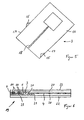
- FIG. 1 shows a module 1, which consists of a transmission module 2 and a chip module 3 is composed. The connection between the transmission module 2 and the chip module 3 takes place in a contacting area of the same.
- the transmission module 2 from a transfer carrier layer 4, on which a transfer element 5 as structured, in particular etching technology, Printing or laser-structured, printed coil printed or is applied as a wire-wound coil.
- the Transmission element 5 is designed as an antenna and is used for Data and / or energy transmission between one in FIG. 3 shown chip 6 and an external device. That several turns having transmission element 5 has at its ends flat contact elements 7. Alternatively, the contact elements 7 can also be round or raised.
- the transmission module 2 has a cutout 8 on, which are adjacent to that formed by the contact elements 7 Contacting area.
- the transfer carrier layer 4 is made of a flexible plastic material PVC, PC or ABS with a thickness of at least 150 microns, preferably 200 to 300 ⁇ m.
- a chip module 3 consists of one thin cuboidal chip carrier layer 10, which is preferably is formed from a metallic material.
- the integrated circuit 6 is applied to the chip carrier layer 10, its electrical connections through contact elements 11 be formed.
- the contact elements 11 are crown-shaped Cutting contacts 12 with protruding at right angles and tapering Jagged 13 formed.
- the formation of the contact elements 11 is carried out by appropriate cutting and bending tools. By punching 9, the contact elements 11 are apart separated and isolated.
- the chip module 3 can be used as an intermediate product be kept ready on a roll.
- the press fit is increased by the thickness the point 13 is substantially larger than the thickness of the contact elements 7, preferably twice as large as the transverse extent the contact elements 7. It becomes a permanent clamping connection created between the contact elements 7 and 11, wherein a predetermined by the thickness of the contact elements 7 and 11 Majesty of module 1 is formed.
- the chip carrier layer 10 can only have incisions, in particular cross-shaped incisions. Only at the Establishing the connection between the chip module 3 and the Transmission module 2 is by tipping or swiveling the through the incisions formed prongs 13 from one with the Chip carrier layer 10 common level, the contact element 11 formed, which then corresponds to the contact element 7 in plant brought. In this embodiment, formation occurs the cutting contacts 12 so only immediately when connected of the chip module 3 with the transmission module 2. The chip module 3 can thus essentially without protruding contact elements 11 are kept ready, so that the manufacturing Effort is reduced.
- the contact elements are designed as contact lugs 15.
- the contact lugs 15 each correspond to a corresponding one Contact surface of the transmission module on one edge 17 of a chip carrier layer 16 is arranged.
- the contact lugs 15 are triangular. Alternatively, they can also be designed in the form of an arc. It is important that the area of the contact elements 15 is so large is that after bending the same a sufficiently large contact area is formed, which is flat on the corresponding Contact element of the transmission module rests.
- a slot 18 separates the contact elements 15 from one another, so that there is no electrical connection between them.
- the contact elements of the chip module can also be used the provision of marginal incisions in a cuboid Chip carrier layer are formed, so less material is required.
- the formation of at least one contact element are formed by the course of the insulating slot, so that the manufacturing outlay is further reduced can be.
- the contact elements can therefore on any Place of the chip carrier layer may be arranged, preferably but in an edge area. They are part of the chip carrier layer formed so that the chip carrier layer has a double Function. On the one hand, it serves as a carrier layer for the chip and the other to form contact elements.
- the chip carrier layer is made of an electrically conductive material formed, preferably from sheet metal.
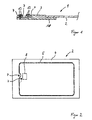
- the modules described above serve as semi-finished products for the production of a chip card 19, as shown in Figure 6 is.
- the chip card 19 can be produced in the laminating technology , each being adjacent to the transfer carrier layer 4 and the chip carrier layer 10 an inner Core layer 20 connects.
- the core layers 20 each have to the elevations of the transfer carrier layer 4 and the chip carrier layer 10 corresponding recesses 21.
- the core layers 20 and the cover layers 22 can consist of an ABS, PC or PVC material.
Landscapes
- Engineering & Computer Science (AREA)
- Microelectronics & Electronic Packaging (AREA)
- Computer Hardware Design (AREA)
- Physics & Mathematics (AREA)
- General Physics & Mathematics (AREA)
- Theoretical Computer Science (AREA)
- Manufacturing & Machinery (AREA)
- Credit Cards Or The Like (AREA)
Abstract
Description
- Figur 1
- Einen Teillängsschnitt durch ein Modul,
- Figur 2
- eine Draufsicht auf ein Übertragungsmodul,
- Figur 3
- eine perspektivische Ansicht eines Chipmoduls nach einem ersten Ausführungsbeispiel,
- Figur 4
- einen Querschnitt durch ein Kontaktelement gemäß Figur 3,
- Figur 5
- eine perspektivische Ansicht auf ein Chipmodul mit Kontaktelementen nach einem zweiten Ausführungsbeispiel und
- Figur 6
- einen Längsschnitt durch eine Chipkarte mit einem erfindungsgemäßen Modul.
Claims (6)
- Modul, insbesondere zur Verwendung in Chipkarten, enthaltend ein Chipmodul (3) mit einem integrierten Schaltkreis (6) einerseits und ein Übertragungsmodul (2) mit einem Übertragungselement (5) zur Datenund/oder Energieübertragung zwischen dem integrierten Schaltkreis (6) und einem externen Gerät oder vice versa andererseits, wobei das Chipmodul (3) und das Übertragungsmodul (2) jeweils Trägerschichten (4, 10) und Kontaktelemente (7, 11) zur elektrischen Verbindung miteinander aufweisen, wobei das Chipmodul (3) oder das Übertragungsmodul (2) verbiegbare Verbindungselemente (12) aufweist zur formschlüssigen mechanischen und elektrischen Verbindung miteinander, wobei das Verbindungselement (12) an einer Seite der Trägerschicht (4, 10) klemmend anlegbar ist, dadurch gekennzeichnet, dass das Verbindungselement (12) als ein solches Schneidelement ausgebildet ist, dass es nach dem Hindurchdrücken durch die Trägerschicht (4, 10) des Chipmoduls (3) bzw. des Übertragungsmoduls (2) unter flächiger Anlage des Chipmoduls (3) an dem Übertragungsmodul (2) anlegbar ist.
- Modul nach Anspruch 1, dadurch gekennzeichnet, dass das Schneidelement (12) als Kontaktelement (11) des Chipmoduls (3) ausgebildet ist und abragende Zacken (13) aufweist, die in der Kontaktierungsposition unter Verbiegung derselben an dem korrespondierenden Kontaktelement (7) des Übertragungsmoduls (2) anliegen.
- Modul nach Anspruch 1 oder 2, dadurch gekennzeichnet, dass das Chipmodul (3) eine aus einem metallischen Werkstoff bestehende Chipträgerschicht (10) aufweist, wobei die Kontaktelemente (11) des Chipmoduls (3) jeweils einstückig mit der Chipträgerschicht (10) verbunden sind.
- Modul nach einem der Ansprüche 1 bis 3, dadurch gekennzeichnet, dass die Chipträgerschicht (10) aus einem Blechmaterial besteht, wobei die Kontaktelemente (11) des Chipmoduls (3) durch Ausstanzen gebildet sind.
- Modul nach einem der Ansprüche 1 bis 4, dadurch gekennzeichnet, dass die Kontaktelemente (11) des Chipmoduls (3) randseitig am Chipmodul (3) als abstehende Kontaktlappen (15) angeordnet sind.
- Verwendung eines Moduls nach einem der Ansprüche 1 bis 5 in einer Chipkarte.
Applications Claiming Priority (5)
| Application Number | Priority Date | Filing Date | Title |
|---|---|---|---|
| DE19732409 | 1997-07-28 | ||
| DE19732409 | 1997-07-28 | ||
| DE19733777A DE19733777C2 (de) | 1997-07-28 | 1997-08-05 | Modul und Verfahren zur Herstellung eines Moduls sowie eine Chipkarte |
| DE19733777 | 1997-08-05 | ||
| PCT/DE1998/002097 WO1999005643A2 (de) | 1997-07-28 | 1998-07-25 | Chipmodul, modul und verfahren zur herstellung eines moduls sowie eine chipkarte |
Publications (2)
| Publication Number | Publication Date |
|---|---|
| EP0998723A2 EP0998723A2 (de) | 2000-05-10 |
| EP0998723B1 true EP0998723B1 (de) | 2003-04-09 |
Family
ID=26038634
Family Applications (1)
| Application Number | Title | Priority Date | Filing Date |
|---|---|---|---|
| EP98947338A Expired - Lifetime EP0998723B1 (de) | 1997-07-28 | 1998-07-25 | Modul und seine verwendung in einer chipkarte |
Country Status (6)
| Country | Link |
|---|---|
| EP (1) | EP0998723B1 (de) |
| JP (1) | JP2001511571A (de) |
| CN (1) | CN1265213A (de) |
| AU (1) | AU9431098A (de) |
| BR (1) | BR9815494A (de) |
| WO (1) | WO1999005643A2 (de) |
Families Citing this family (4)
| Publication number | Priority date | Publication date | Assignee | Title |
|---|---|---|---|---|
| JP4712157B2 (ja) * | 2000-05-08 | 2011-06-29 | 大日本印刷株式会社 | 非接触式データキャリア |
| JP4783991B2 (ja) * | 2001-03-28 | 2011-09-28 | 大日本印刷株式会社 | Icモジュールの製造方法 |
| DE102013018518A1 (de) * | 2013-11-04 | 2015-05-07 | Giesecke & Devrient Gmbh | IC-Modul für unterschiedliche Verbindungstechniken |
| DE102014012394A1 (de) * | 2014-08-21 | 2016-02-25 | Giesecke & Devrient Gmbh | Datenträger mit Teilstück |
Citations (1)
| Publication number | Priority date | Publication date | Assignee | Title |
|---|---|---|---|---|
| US5598032A (en) * | 1994-02-14 | 1997-01-28 | Gemplus Card International | Hybrid chip card capable of both contact and contact-free operation and having antenna contacts situated in a cavity for an electronic module |
Family Cites Families (3)
| Publication number | Priority date | Publication date | Assignee | Title |
|---|---|---|---|---|
| DE4440721A1 (de) * | 1994-11-15 | 1996-05-23 | Datacolor Druck Und Fullservic | Trägerelement für IC-Baustein |
| EP0917688B1 (de) * | 1996-08-02 | 2000-06-28 | SCHLUMBERGER Systèmes | Kombinierte chipkarte |
| DE29706016U1 (de) * | 1997-04-04 | 1998-08-06 | TELBUS Gesellschaft für elektronische Kommunikations-Systeme mbH, 85391 Allershausen | Elektronisches Gerät, insbesondere Chipkarte mit Nietverbindung |
-
1998
- 1998-07-25 EP EP98947338A patent/EP0998723B1/de not_active Expired - Lifetime
- 1998-07-25 WO PCT/DE1998/002097 patent/WO1999005643A2/de not_active Ceased
- 1998-07-25 CN CN 98807596 patent/CN1265213A/zh active Pending
- 1998-07-25 AU AU94310/98A patent/AU9431098A/en not_active Abandoned
- 1998-07-25 BR BR9815494-0A patent/BR9815494A/pt not_active Application Discontinuation
- 1998-07-25 JP JP2000504548A patent/JP2001511571A/ja not_active Withdrawn
Patent Citations (1)
| Publication number | Priority date | Publication date | Assignee | Title |
|---|---|---|---|---|
| US5598032A (en) * | 1994-02-14 | 1997-01-28 | Gemplus Card International | Hybrid chip card capable of both contact and contact-free operation and having antenna contacts situated in a cavity for an electronic module |
Also Published As
| Publication number | Publication date |
|---|---|
| CN1265213A (zh) | 2000-08-30 |
| WO1999005643A2 (de) | 1999-02-04 |
| BR9815494A (pt) | 2000-10-31 |
| EP0998723A2 (de) | 2000-05-10 |
| WO1999005643A3 (de) | 1999-04-08 |
| AU9431098A (en) | 1999-02-16 |
| JP2001511571A (ja) | 2001-08-14 |
Similar Documents
| Publication | Publication Date | Title |
|---|---|---|
| DE2234960C3 (de) | Elektrischer Stecker | |
| EP0869453B1 (de) | Verfahren zur Herstellung einer Chipkarte | |
| DE69901712T2 (de) | Perforierte antenne für ic karte und ic karte mit solcher antenne | |
| EP1216453B1 (de) | Verfahren zur herstellung einer chipkarte und nach dem verfahren hergestellte chipkarte | |
| DE69702399T2 (de) | Kombinierte chipkarte | |
| DE69905288T2 (de) | Verfahren zur herstellung einer kontaktlosen chipkarte | |
| DE3904827A1 (de) | Elektrischer steckverbinder | |
| WO2013152840A1 (de) | Transponderlage und verfahren zu deren herstellung | |
| DE2234961B2 (de) | Verfahren zur Herstellung von Steckern für Schaltplatten | |
| EP1877967B1 (de) | Verfahren zur herstellung eines tragbaren datenträgers | |
| DE19625228C2 (de) | Systemträger für die Montage einer integrierten Schaltung in einem Spritzgußgehäuse | |
| EP0998723B1 (de) | Modul und seine verwendung in einer chipkarte | |
| EP1523069A1 (de) | Kontaktfeder für einen Antennenverstärker | |
| DE3005634A1 (de) | Steckverbindung | |
| DE4332927C2 (de) | Piezo-Schaltelement | |
| WO2012146754A1 (de) | Kontaktstabiler schnappverbinder | |
| DE19733777C2 (de) | Modul und Verfahren zur Herstellung eines Moduls sowie eine Chipkarte | |
| DE1590564A1 (de) | Verfahren und Vorrichtung zur Herstellung gedruckter Schaltungsplatten | |
| DE102009050386B4 (de) | Verfahren zum Herstellen von Durchkontaktierungen | |
| DE10234751B4 (de) | Verfahren zur Herstellung einer spritzgegossenen Chipkarte und nach dem Verfahren hergestellte Chipkarte | |
| WO2001016876A2 (de) | Chipkarte und verfahren zur herstellung einer chipkarte | |
| DE3231380C2 (de) | Verfahren zur Herstellung eines elektrischen Anschlusses | |
| DE19840501C1 (de) | Kontaktierungsvorrichtung aus elastischem Material | |
| DE102012214121A1 (de) | Elektrische Kontaktierung mit Schneidkante | |
| DE102004011601B4 (de) | Trägerplatte mit einer Kontaktfeder für Antennenverstärker |
Legal Events
| Date | Code | Title | Description |
|---|---|---|---|
| PUAI | Public reference made under article 153(3) epc to a published international application that has entered the european phase |
Free format text: ORIGINAL CODE: 0009012 |
|
| 17P | Request for examination filed |
Effective date: 20000222 |
|
| AK | Designated contracting states |
Kind code of ref document: A2 Designated state(s): BE CH DE ES FR GB IT LI NL |
|
| 17Q | First examination report despatched |
Effective date: 20010131 |
|
| RTI1 | Title (correction) |
Free format text: MODULE AND ITS USE IN A CHIP CARD |
|
| GRAG | Despatch of communication of intention to grant |
Free format text: ORIGINAL CODE: EPIDOS AGRA |
|
| RIN1 | Information on inventor provided before grant (corrected) |
Inventor name: WENDISCH, KARL-HEINZ |
|
| GRAG | Despatch of communication of intention to grant |
Free format text: ORIGINAL CODE: EPIDOS AGRA |
|
| GRAH | Despatch of communication of intention to grant a patent |
Free format text: ORIGINAL CODE: EPIDOS IGRA |
|
| RAP1 | Party data changed (applicant data changed or rights of an application transferred) |
Owner name: WENDISCH, KARL-HEINZ |
|
| RIN1 | Information on inventor provided before grant (corrected) |
Inventor name: WENDISCH, KARL-HEINZ |
|
| GRAH | Despatch of communication of intention to grant a patent |
Free format text: ORIGINAL CODE: EPIDOS IGRA |
|
| GRAA | (expected) grant |
Free format text: ORIGINAL CODE: 0009210 |
|
| AK | Designated contracting states |
Designated state(s): BE CH DE ES FR GB IT LI NL |
|
| PG25 | Lapsed in a contracting state [announced via postgrant information from national office to epo] |
Ref country code: NL Free format text: LAPSE BECAUSE OF FAILURE TO SUBMIT A TRANSLATION OF THE DESCRIPTION OR TO PAY THE FEE WITHIN THE PRESCRIBED TIME-LIMIT Effective date: 20030409 Ref country code: IT Free format text: LAPSE BECAUSE OF FAILURE TO SUBMIT A TRANSLATION OF THE DESCRIPTION OR TO PAY THE FEE WITHIN THE PRE;WARNING: LAPSES OF ITALIAN PATENTS WITH EFFECTIVE DATE BEFORE 2007 MAY HAVE OCCURRED AT ANY TIME BEFORE 2007. THE CORRECT EFFECTIVE DATE MAY BE DIFFERENT FROM THE ONE RECORDED.SCRIBED TIME-LIMIT Effective date: 20030409 |
|
| REG | Reference to a national code |
Ref country code: GB Ref legal event code: FG4D Free format text: NOT ENGLISH |
|
| REG | Reference to a national code |
Ref country code: CH Ref legal event code: EP |
|
| PG25 | Lapsed in a contracting state [announced via postgrant information from national office to epo] |
Ref country code: LI Free format text: LAPSE BECAUSE OF NON-PAYMENT OF DUE FEES Effective date: 20030731 Ref country code: CH Free format text: LAPSE BECAUSE OF NON-PAYMENT OF DUE FEES Effective date: 20030731 Ref country code: BE Free format text: LAPSE BECAUSE OF NON-PAYMENT OF DUE FEES Effective date: 20030731 |
|
| NLV1 | Nl: lapsed or annulled due to failure to fulfill the requirements of art. 29p and 29m of the patents act | ||
| GBT | Gb: translation of ep patent filed (gb section 77(6)(a)/1977) | ||
| PG25 | Lapsed in a contracting state [announced via postgrant information from national office to epo] |
Ref country code: ES Free format text: LAPSE BECAUSE OF FAILURE TO SUBMIT A TRANSLATION OF THE DESCRIPTION OR TO PAY THE FEE WITHIN THE PRESCRIBED TIME-LIMIT Effective date: 20031030 |
|
| ET | Fr: translation filed | ||
| BERE | Be: lapsed |
Owner name: *WENDISCH KARL-HEINZ Effective date: 20030731 |
|
| PLBE | No opposition filed within time limit |
Free format text: ORIGINAL CODE: 0009261 |
|
| STAA | Information on the status of an ep patent application or granted ep patent |
Free format text: STATUS: NO OPPOSITION FILED WITHIN TIME LIMIT |
|
| REG | Reference to a national code |
Ref country code: CH Ref legal event code: PL |
|
| 26N | No opposition filed |
Effective date: 20040112 |
|
| REG | Reference to a national code |
Ref country code: FR Ref legal event code: TP |
|
| REG | Reference to a national code |
Ref country code: GB Ref legal event code: 732E |
|
| REG | Reference to a national code |
Ref country code: FR Ref legal event code: TP Ref country code: FR Ref legal event code: CD Ref country code: FR Ref legal event code: CA |
|
| REG | Reference to a national code |
Ref country code: GB Ref legal event code: 732E Free format text: REGISTERED BETWEEN 20110113 AND 20110119 |
|
| PGFP | Annual fee paid to national office [announced via postgrant information from national office to epo] |
Ref country code: GB Payment date: 20120723 Year of fee payment: 15 |
|
| PGFP | Annual fee paid to national office [announced via postgrant information from national office to epo] |
Ref country code: FR Payment date: 20120803 Year of fee payment: 15 |
|
| GBPC | Gb: european patent ceased through non-payment of renewal fee |
Effective date: 20130725 |
|
| REG | Reference to a national code |
Ref country code: FR Ref legal event code: ST Effective date: 20140331 |
|
| PG25 | Lapsed in a contracting state [announced via postgrant information from national office to epo] |
Ref country code: GB Free format text: LAPSE BECAUSE OF NON-PAYMENT OF DUE FEES Effective date: 20130725 |
|
| PG25 | Lapsed in a contracting state [announced via postgrant information from national office to epo] |
Ref country code: FR Free format text: LAPSE BECAUSE OF NON-PAYMENT OF DUE FEES Effective date: 20130731 |
|
| PGFP | Annual fee paid to national office [announced via postgrant information from national office to epo] |
Ref country code: DE Payment date: 20170724 Year of fee payment: 20 |
|
| REG | Reference to a national code |
Ref country code: DE Ref legal event code: R071 Ref document number: 59807885 Country of ref document: DE |